

®
ICM7211AM
Data Sheet FN3158.7April 17, 2006
4-Digit, LCD Display Driver
The ICM7211AM device is a non-multiplexed four-digit
seven-segment CMOS LCD display decoder-driver.
This device is configured to drive conventional LCD displays
by providing a complete RC oscillator, divider chain,
backplane driver, and 28 segment outputs.
It also has a microprocessor compatible input configuration,
which provides data input latches and Digit Address latches
under control of high-speed Chip Select inputs. These devices
simplify the task of implementing a cost-effective
alphanumeric seven-segment display for microprocessor
Features
• Four Digit Non-Multiplexed 7 Segment LCD Display
Outputs with Backplane Driver
• Complete Onboard RC Oscillator to Generate Backplane
Frequency
• Backplane Input/Output Allows Simple Synchronization of
Slave-Devices to a Master
• Provides Data and Digit Address Latches Controlled by
Chip Select Inputs to Provide a Direct High Speed
Processor Interface
• Decodes Binary to Code B (0-9, Dash, E, H, L, P, Blank)
systems, without requiring extensive ROM or CPU time for
decoding and display updating.
• Pb-Free Plus Anneal Available (RoHS Compliant)
The ICM7211AM provides the “Code B” output code, i.e.,
0-9, dash, E, H, L, P, blank, but will correctly decode true
BCD to seven-segment decimal outputs.
Ordering Information
DISPLA Y
PART NUMBER PART MARKING
ICM7211AMlM44 ICM7211AMlM44 LCD Code B Microprocessor Direct Drive -40 to 85 44 Ld MQFP Q44.10x10
ICM7211AMlPL ICM7211AMlPL LCD Code B Microprocessor Direct Drive -40 to 85 40 Ld PDIP E40.6
ICM7211AMlPLZ
(Note)
NOTE: Intersil Pb-free plus anneal products employ special Pb-free material sets; molding compounds/die attach materials and 100% matte tin plate
termination finish, which are RoHS compliant and compatible with both SnPb and Pb-free soldering operations. Intersil Pb-free products are MSL
classified at Pb-free peak reflow temperatures that meet or exceed the Pb-free requirements of IPC/JEDEC J STD-020.
*Pb-free PDIPs can be used for through hole wave solder processing only. They are not intended for use in Reflow solder processing applications.
ICM7211AMlPLZ LCD Code B Microprocessor Direct Drive -40 to 85 40 Ld PDIP*
TYPE
DISPLAY
DECODING
INPUT
INTERFACING
DISPLAY
DRIVE TYPE
TEMP.
RANGE ( ° C) PACKAGE
(Pb-free)
PKG.
DWG. #
E40.6
1
CAUTION: These devices are sensitive to electrostatic discharge; follow proper IC Handling Procedures.
1-888-INTERSIL or1-888-468-3774
| Intersil (and design) is a registered trademark of Intersil Americas Inc.
Copyright Intersil Americas Inc. 2001, 2004-2006. All Rights Reserved
All other trademarks mentioned are the property of their respective owners.
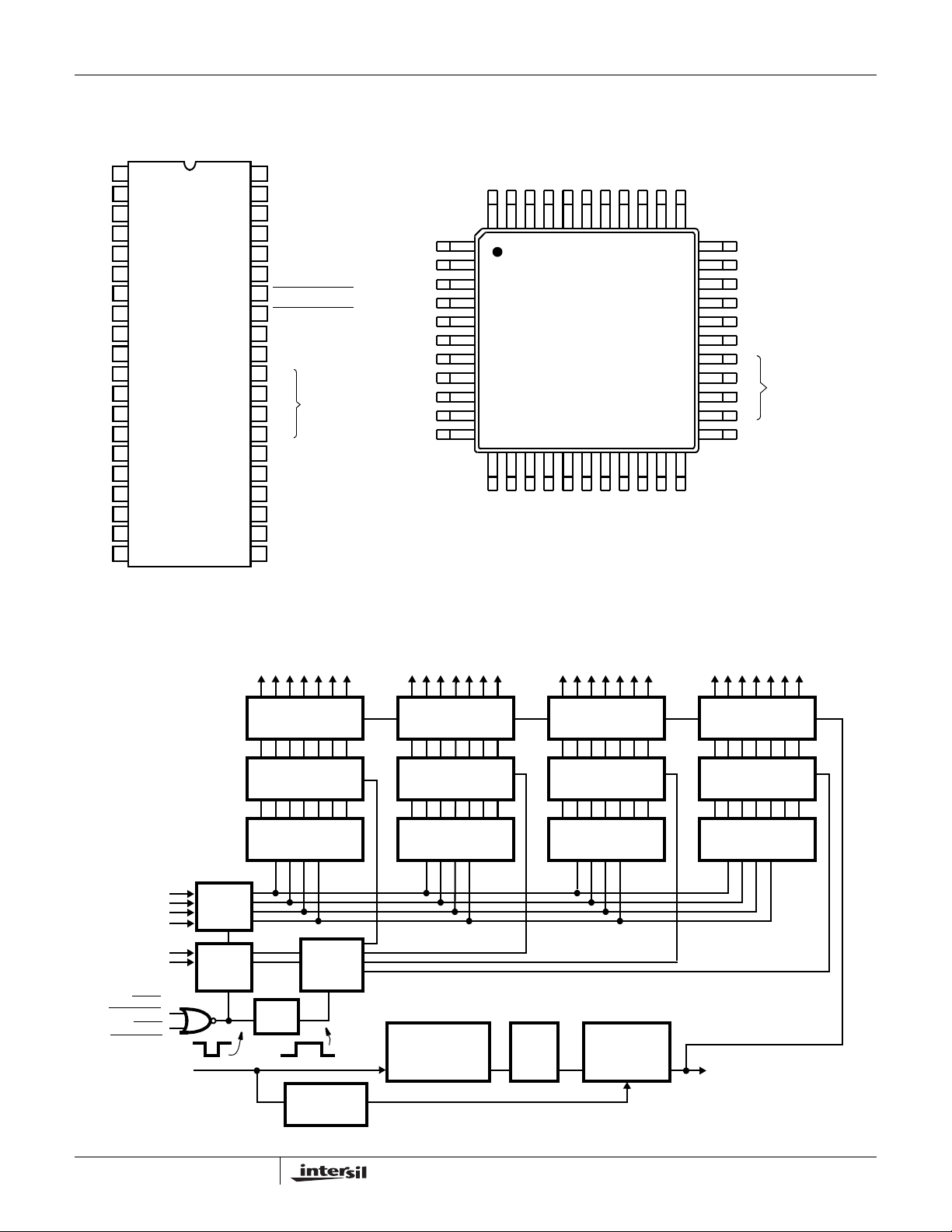
Pinouts
ICM7211AM (PDIP)
TOP VIEW
ICM7211AMICM7211AM
ICM7211AM (MQFP)
TOP VIEW
1
V
DD
2
e1
3
g1
4
f1
5
BP
6
a2
7
b2
8
c2
9
d2
10
e2
11
g2
12
f2
13
a3
14
b3
15
c3
16
d3
17
e3
18
g3
19
f3
20
a4
40
d1
39
c1
38
b1
37
a1
OSC
36
V
35
SS
CHIP SELECT 2
34
CHIP SELECT 1
33
DIGIT ADRESS BIT 2
32
DIGIT ADRESS BIT 1
31
B3
30
B2
29
B1
28
B0
27
26
f4
25
g4
24
e4
23
d4
22
c4
21
b4
Functional Block Diagram
SEGMENT OUTPUTS
DATA
INPUTS
D4
BPf1g1e1V
44 43 42 41 40
a2
b2
c2
d2
e2
NC
g2
f2
a3
b3
c3
1
2
3
4
5
6
7
8
9
10
11
12 13 14 15 16 17
d3e3g3
ICM7211AM
SEGMENT OUTPUTS
D3
DD
NCd1c1b1a1
39 38 37 36 35 34
f3
a4
b4c4d4e4g4
NC
SEGMENT OUTPUTS
D2
OSC
33
32
31
30
29
28
27
26
25
24
23
2221201918
SEGMENT OUTPUTS
V
SS
CHIP SELECT 2
CHIP SELECT 1
DIGITAL ADDRESS BIT 2
DIGITAL ADDRESS BIT 2
NC
B3
B2
DATA
INPUTS
B1
B0
f4
D1
DATA
INPUTS
2-BIT
DIGIT
ADRESS
INPUT
CHIP
SELECT 1
CHIP
SELECT 2
OSCILLATOR
INPUT
4-BIT
LATCH
ENABLE
2-BIT
LATCH
ENABLE
7 WIDE DRIVER
7 WIDE LATCH EN
PROGRAMMABLE
4 TO 7 DECODER
2 TO 4
DECODER
ONE
SHOT
ENABLE
DIRECTOR
2
7 WIDE DRIVER
7 WIDE LATCH EN
PROGRAMMABLE
4 TO 7 DECODER
OSCILLATOR
19kHz
FREE-RUNNING
7 WIDE LATCH EN
PROGRAMMABLE
4 TO 7 DECODER
÷128
7 WIDE DRIVER
BLACKPLANE
DRIVER
ENABLE
7 WIDE DRIVER
7 WIDE LATCH EN
PROGRAMMABLE
4 TO 7 DECODER
BP INPUT/OUTPUT
FN3158.7
April 17, 2006
ICM7211AMICM7211AM
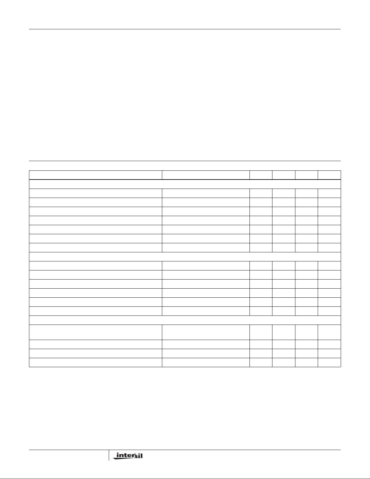
Absolute Maximum Ratings Thermal Information
Supply Voltage (VDD - VSS) . . . . . . . . . . . . . . . . . . . . . . . . . . . 6.5V
Input Voltage (Any Terminal) (Note 1) . . .V
- 0.3V to VDD, + 0.3V
SS
Operating Conditions
Temperature Range. . . . . . . . . . . . . . . . . . . . . . . . . . .-40°C to 85°C
CAUTION: Stresses above those listed in “Absolute Maximum Ratings” may cause permanent damage to the device. This is a stress only rating and operation of the
device at these or any other conditions above those indicated in the operational sections of this specification is not implied.
NOTES:
1. Due to the SCR structure inherent in the CMOS process, connecting any terminal to voltages greater than V
destructive device latchup. For this reason, it is recommended that no inputs from external sources not operating on the same power supply be
applied to the device before its supply is established, and that in multiple supply systems, the supply to the ICM7211AM be turned on first.
2. θ
is measured with the component mounted on an evaluation PC board in free air.
JA
Electrical Specifications
PARAMETER TEST CONDITIONS MIN TYP MAX UNITS
CHARACTERISTICS V
Operating Supply Voltage Range (V
Operating Current, I
Oscillator Input Current, I
Segment Rise/Fall Time, t
Backplane Rise/Fall Time, t
Oscillator Frequency, f
Backplane Frequency, f
INPUT CHARACTERISTICS
Logical “1” Input Voltage, V
Logical “0” Input Voltage, V
Input Leakage Current, I
Input Capacitance, C
BP/Brightness Input Leakage, I
BP/Brightness Input Capacitance, C
AC CHARACTERISTICS
Chip Select Active Pulse Width, t
Data Setup Time, t
Data Hold Time, t
DH
Inter-Chip Select Time, t
= 5V ±10%, TA = 25°C, VSS = 0V Unless Otherwise Specified
DD
- VSS), V
DD
OSC
lN
BP
ILK
OSCI
, t
r
r
IH
IL
DD
f
, t
f
BPLK
BPI
WL
SUPPLY
Test circuit, Display blank - 10 50 µA
Pin 36 - ±2 ±10 µA
CL = 200pF - 0.5 - µs
CL = 5000pF - 1.5 - µs
Pin 36 Floating - 19 - kHz
Pin 36 Floating - 150 - Hz
Pins 27-34 - ±0.01 ±1 µA
Pins 27-34 - 5 - pF
Measured at Pin 5 with Pin 36 at V
All Devices - 200 - pF
Other Chip Select Either Held Active, or
Both Driven Together
DS
ICS
Thermal Resistance (Typical, Note 2)
θ
JA
(°C/W)
PDIP Package* . . . . . . . . . . . . . . . . . . . . . . . . . . . . 60
MQFP Package . . . . . . . . . . . . . . . . . . . . . . . . . . . . 70
Maximum Junction Temperature . . . . . . . . . . . . . . . . . . . . . . . 150°C
Maximum Storage Temperature Range . . . . . . . . .-65×°C to 150°C
Maximum Lead Temperature (Soldering, 10s) . . . . . . . . . . . . 300°C
*Pb-free PDIPs can be used for through hole wave solder processing only. They are not intended for use in Reflow solder processing
applications.
or less than VSS may cause
DD
356 V
4--V
--1V
SS
- ±0.01 ±1 µA
200 - - ns
100 - - ns
10 0 - ns
2--µs
3
FN3158.7
April 17, 2006

ICM7211AMICM7211AM
Input Definitions In this table, V
and VSS are considered to be normal operating input logic levels. Actual input low and high levels are specified
DD
under Operating Characteristics. For lowest power consump tion, input sign als should swing over the full su pply.
INPUT DIP TERMINAL CONDITIONS FUNCTION
B0 27 V
B1 28 V
B2 29 V
B3 30 VDD = Logical One
OSC 36 Floating or with External
= Logical One
DD
V
= Logical Zero
SS
= Logical One
DD
V
= Logical Zero
SS
= Logical One
DD
V
= Logical Zero
SS
V
= Logical Zero
SS
Capacitor to V
V
SS
Ones (Least Significant)
Twos
Fours
Eights (Most Significant)
Oscillator Input
DD
Disables BP output devices, allowing segments to be synchronized to an
external signal input at the BP terminal (Pin 5).
Interface Input Configuration
INPUT DESCRIPTION DIP TERMINAL CONDITIONS FUNCTION
DA1 Digit Address
31 V
Bit 1 (LSB)
DA2 Digit Address
32 V
Bit 2 (MSB)
Chip Select 1 33 VDD = Inactive
CS1
CS2
Chip Select 2 34 VDD = Inactive
= Logical One
DD
V
= Logical Zero
SS
= Logical One
DD
V
= Logical Zero
SS
V
= Active
SS
V
= Active
SS
DA1 and DA2 serve as a 2-bit Digit Address Input
DA2, DA1 = 00 selects D4
DA2, DA1 = 01 selects D3
DA2, DA1 = 10 selects D2
DA2, DA1 = 11 selects D1
When both CS1
and CS2 are taken low, the data at the Data and Digit
Select code inputs are written into the input latches. On the rising edge
of either Chip Select
, the data is decoded and written into the output
latches.
Data Input Bits
Timing Diagram
DATA AND
ADDRESS
CS1
(CS2)
CS2
(CS1)
DIGIT
t
WI
t
DS
= DON’T CARE
t
ICS
t
DH
FIGURE 1. MICROPROCESSOR INTERFACE INPUT
4
FN3158.7
April 17, 2006

Typical Performance Curves
ICM7211AMICM7211AM
30
DISPLA Y BLANK, PIN 36 OPEN
25
4123 675
SUPP
TA = -20°C
TA = 70°C
(V)
20
TA = 25°C
15
(µA)
OP
I
10
5
V
FIGURE 2. OPERATING SUPPLY CURRENT AS A FUNCTION
OF SUPPLY VOLTAGE
180
TA = 25°C
150
120
(Hz)
90
BP
ƒ
60
30
0
C
= 0pF
OSC
(PIN 36 OPEN)
V
SUPP
C
= 22pF
OSC
C
OSC
4123 65
(V)
= 220pF
FIGURE 3. BACKPLANE FREQUENCY AS A FUNCTION OF
SUPPLY VOLTAGE
5
FN3158.7
April 17, 2006

ICM7211AMICM7211AM
Description of Operation
Device
The ICM7211AM provides outputs suitable for driving
conventional four-digit, seven-segment LCD displays. These
devices include 28 individual segment drivers, backplane
driver, and a self-contained oscillator and divider chain to
generate the backplane frequency.
The segment and backplane drivers each consist of a
CMOS inverter, with the N-Channel and P-Channel devices
ratioed to provide identical on resistances, and thus equal
rise and fall times. This eliminates any DC component, which
could arise from differing rise and fall times, and ensures
maximum display life.
The backplane output devices can be disabled by
connecting the OSCillator input (pin 36) to V
the 28 segment outputs to be synchronized directly to a
signal input at the BP terminal (pin 5). In this manner,
several slave devices may be cascaded to the backplane
output of one master device, or the backplane may be
derived from an external source. This allows the use of
displays with characters in multiples of four and a single
backplane. A slave device represents a load of
approximately 200pF (comparable to one additional
segment). Thus the limitation of the number of devices that
can be slaved to one master device backplane driver is the
additional load represented by the larger backplane of
displays of more than four digits. A good rule of thumb to
observe in order to minimize power consumption is to keep
the backplane rise and fall times less than about 5µs. The
backplane output driver should handle the backplane to a
display of 16 one-half inch characters. It is recommended, if
more than four devices are to be slaved together, the
backplane signal be derived externally and all the
ICM7211AM devices be slaved to it. This external signal
should be capable of driving very large capacitive loads with
short (1 - 2µs) rise and fall times. The maximum frequency
for a backplane signal should be about 150Hz although this
may be too fast for optimum display response at lower
display temperatures, depending on the display type.
. This allows
SS
Another technique for overdriving the oscillator (with a signal
swinging the full supply) is to skew the duty cycle of the
overdriving signal such that the negative portion has a duration
shorter than about one microsecond. The backplane disable
sensing circuit will not respond to signals of this duration.
OSCILLATOR
FREQUENCY
BACKPLANE
INPUT/OUTPUT
OFF
SEGMENTS
ON
SEGMENTS
FIGURE 4. DISPLAY WAVEFORMS
128 CYCLES
64 CYCLES
64 CYCLES
Input Configurations and Output Codes
The ICM7211AM accepts a four-bit true binary (i.e., positive
level = logical one) input at pins 27 thru 30, least significant
bit at pin 27 ascending to the most significant bit at pin 30. It
decodes the binary input into seven-segment alphanumeric
“Code B” output, i.e., 0-9, dash, E, H, L, P, blank. These
codes are shown explicitly in Table 1. It will correctly decode
true BCD to a seven-segment decimal output.
TABLE 1. OUTPUT CODES
BlNARY
CODE B
ICM7211AMB3 B2 B1 BO
0000
0001
0010
0011
0100
The onboard oscillator is designed to free run at
approximately 19kHz at microampere current levels. The
oscillator frequency is divided by 128 to provide the
backplane frequency, which will be approximately 150Hz
with the oscillator free-running; the oscillator frequency may
be reduced by connecting an external capacitor between the
OSCillator terminal and V
DD
.
The oscillator may also be overdriven if desired, although care
must be taken to ensure that the backplane driver is not
disabled during the negative portion of the overdriving signal
(which could cause a DC component to the display). This can
be done by driving the OSCillator input between the positive
supply and a level out of the range where the backplane disable
is sensed (about one fifth of the supply voltage above V
SS
).
6
0101
0110
0111
1000
1001
1010
1011
FN3158.7
April 17, 2006

ICM7211AMICM7211AM
TABLE 1. OUTPUT CODES (Continued)
BlNARY
CODE B
ICM7211AMB3 B2 B1 BO
1100
1101
1110
1111 BLANK
The ICM7211AM is intended to accept data from a data bus
under processor control.
In these devices, the four data input bits and the two-bit digit
address (DA1 pin 31, DA2 pin 32) are written into input
buffer latches when both chip select inputs (CS1
pin 33, CS2
Test Circuit
V
DD
+ -
pin 34) are taken low. On the rising edge of either chip select
input, the content of the data input latches is decoded and
stored in the output latches of the digit selected by the
contents of the digit address latches.
An address of 00 writes into D4, DA2 = 0, DA1 = 1 writes into
D3, DA2 = 1, DA1 = 0 writes into D2, and 11 writes into D1.
The timing relationships for inputting data are shown in
Figure 1, and the chip select pulse widths and data setup and
hold times are specified under Operating Characteristics.
a
f
b
g
e
c
d
FIGURE 5. SEGMENT ASSIGNMENT
V
SS
EACH SEGMENT
OUTPUT TO
BACKPLANE
WITH A 200pF
CAPACITOR
1
2
3
4
5
6
7
8
9
10
11
12
13
14
15
16
17
18
19
20
V
BP
DD
ICM7211AM
DIGIT/CHIP
SELECT
INPUTS
DATA
INPUTS
FIGURE 6.
OSC
V
SS
40
39
38
37
36
35
34
33
32
31
30
29
28
27
26
25
24
23
22
21
MICROPROCESSOR
V
DD
VERSION
MULTIPLEXED
V
SS
VERSION
V
DD
7
FN3158.7
April 17, 2006

Typical Application
ICM7211AM
8 DIGIT
LCD DISPLAY
INPUT
NC
+5V
40
26
V
CCVDD
2 XTAL1
3 XTAL2
4 RESET
7 EA
5 SS
1 TO
39 T1
6 INT
ALE
11 9 25
80C48
µCOMPUTER
PSEN
PROG
20
V
SS
WR
10 8
P10 27
P17 34
P20 21
P27 38
DB0 12
DB7
RD
HIGH ORDER DIGITS
+5V
28
29
30
I/O
31
32
33
22
23
24
35
36
37
I/O
13
14
15
16
17
18
19
ICM7211AM
1 V
DD
35 V
SS
36 OSC
SEGMENTS
DATA
B0-B3
27 28 29 30
2, 3, 4
6-26
37-40
DS1 DS2 CS1
31 32 33 34
BP 5
CS2
BP 5
DATA
B0-B3
2, 3, 4
6-26
37-40
DS1 DS2 CS1
292827 30
ICM7211AM
LOW ORDER DIGITS
SEGMENTS
CS2
31 32 33 34
1 V
DD
35 V
SS
36 OSC
+5V
FIGURE 7. 80C48 MICROPROCESSOR INTERFACE
All Intersil U.S. products are manufactured, assembled and tested utilizing ISO9000 quality systems.
Intersil Corporation’s quality certifications can be viewed at www.intersil.com/design/quality
Intersil products are sold by description only. Intersil Corporation reserves the right to make changes in circuit design, software and/or specifications at any time without
notice. Accordingly, the reader is cautioned to verify that data sheets are current before placing orders. Information furnished by Intersil is believed to be accurate and
reliable. However, no responsibility is assumed by Intersil or its subsidiaries for its use; nor for any infringements of patents or other rights of third parties which may result
from its use. No license is granted by implicat ion or oth erwise u nde r any p a tent or p at ent r ights of Intersil or its subsidiaries.
For information regarding Intersil Corporation and its products, see www.intersil.com
8
FN3158.7
April 17, 2006
 Loading...