

Page 1
查询ICL7112供应商
January 1998
®
D
W
E
N
R
O
F
D
E
D
N
E
M
M
O
C
E
R
T
O
N
S
N
G
I
S
E
ICL7112
12-Bit, High-Speed,
CMOS µP-Compatible A/D Converter
Features
• 12-Bit Resolution and Accuracy
• No Missing Codes
• Microprocessor Compatible Byte-Organized Buffered
Outputs
• Auto-Zeroed Comparator for Low Offset Voltage
• Low Linearity and Gain Errors
• Low Power Consumption (60mW)
• No Gain or Offset Adjustment Necessary
• Provides 3% Usable Overrange
• Fast Conversion (40µs)
Description
The ICL7112 is a monolithic 12-bit resolution, fast
successive approximation A/D converter. It uses thin film
resistors and CMOS circuitry combined with an on-chip
PROM calibration table to achieve 12-bit linearity without
laser trimming. Special design techniques used in the DAC
and comparator result in high speed operation, while the
fully static silicon-gate CMOS circuitry keeps the power
dissipation very low.
Microprocessor bus interfacing is eased by the use of
standard memory WRite
signals, combined with Chip
digital output pins are byte-organized and three-state gated
for bus interface to 8-bit and 16-bit systems.
The lCL7112 provides separate Analog and Digital grounds
for increased system accuracy. Operating with ±5V supplies,
the lCL7112 accepts 0V to +10V input with a -10V reference
or 0V to -10V input with a +10V reference.
and ReaD cycle timing and control
Select and Address pins. The
Ordering Information
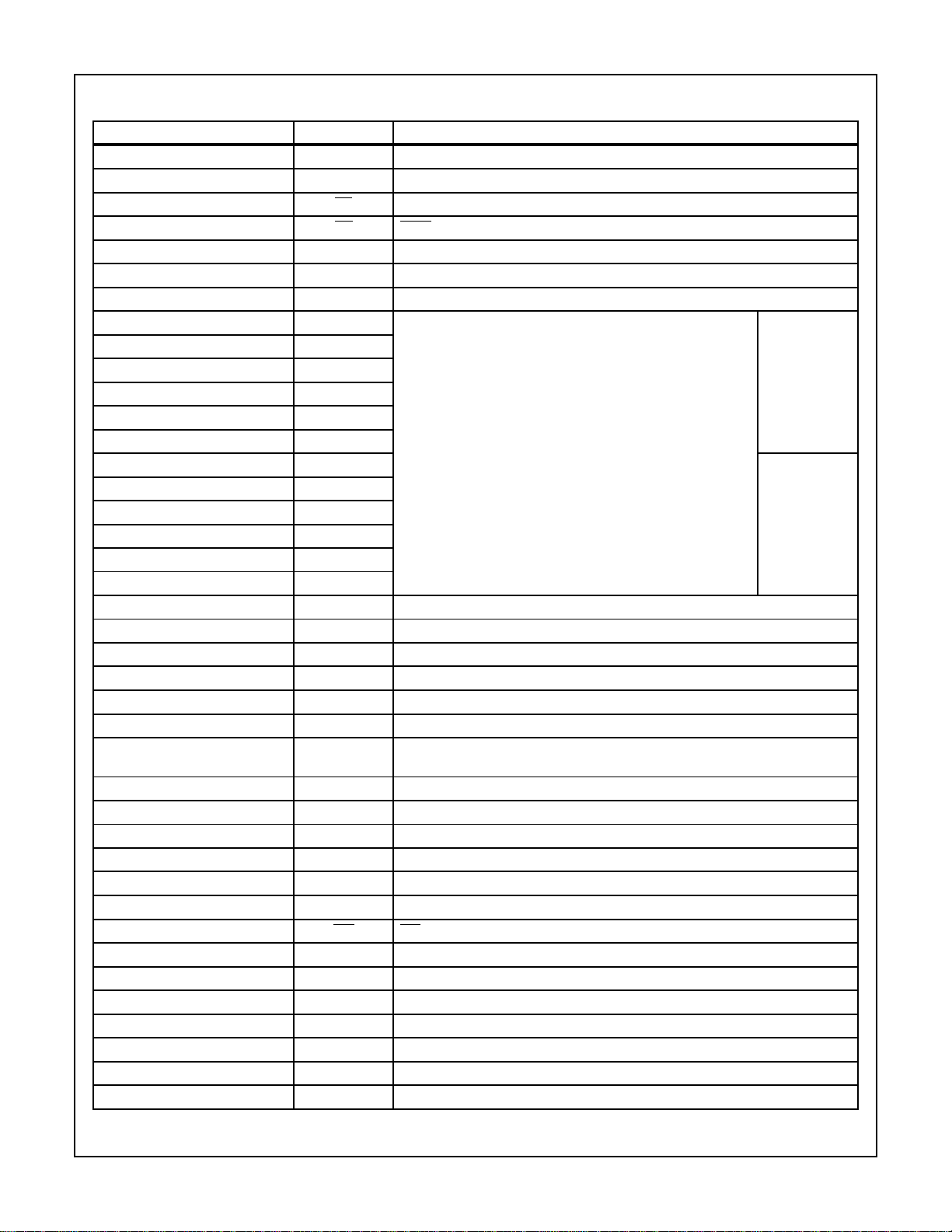
RESOLUTION WITH NO MISSION
PART NO. TEMP. RANGE (oC) PACKAGE
ICL7112JCDL 0 to 70 40 Ld CERDIP 11-Bit
CODES
ICL7112KCDL 0 to 70 40 Ld CERDIP 12-Bit
ICL7112LCDL 0 to 70 40 Ld CERDIP 12-Bit (Note)±
ICL7112JIDL -25 to 85 40 Ld CERDIP 11-Bit
ICL7112KIDL -25 to 85 40 Ld CERDIP 12-Bit
ICL7112LIDL -25 to 85 40 Ld CERDIP 12-Bit (Note)±
ICL7112JMDL -55 to 125 40 Ld CERDIP 11-Bit
ICL7112KMDL -55 to 125 40 Ld CERDIP 12-Bit
ICL7112LMDL -55 to 125 40 Ld CERDIP 12-Bit (Note)±
NOTE: Over operating temperature range.
CAUTION: These devices are sensitive to electrostatic discharge; follow proper IC Handling Procedures.
1-888-INTERSIL or 321-724-71 43
Copyright © Intersil Americas Inc. 2002. All Rights Reserved
| Intersil (and design) is a registered trademark of Intersil Americas Inc.
6-1
File Number 3639.1
Page 2
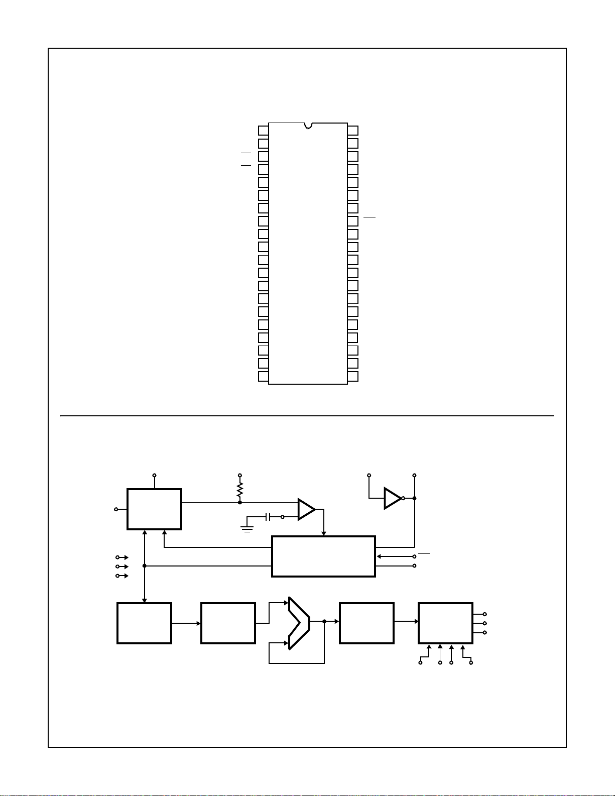
Pinout
AGNDf
DGND
(MSB) D
(LSB) D
NC
CS
RD
A
BUS
D
D
D
D
D
D
D
D
D
D
NC
ICL7112
ICL7112
TOP VIEW
1
2
3
4
5
0
6
7
8
11
9
10
10
9
11
8
12
7
13
6
14
5
15
4
16
3
17
2
18
1
19
0
20
ICL7112
40
39
38
37
36
35
34
33
32
31
30
29
28
27
26
25
24
23
22
21
NC
AGNDs
V
REF
V
IN
COMP
-
V
C
AZ
WR
TEST
OSC2
OSC1
TEST
PROG
+
V
OVR
EOC
NC
NC
NC
NC
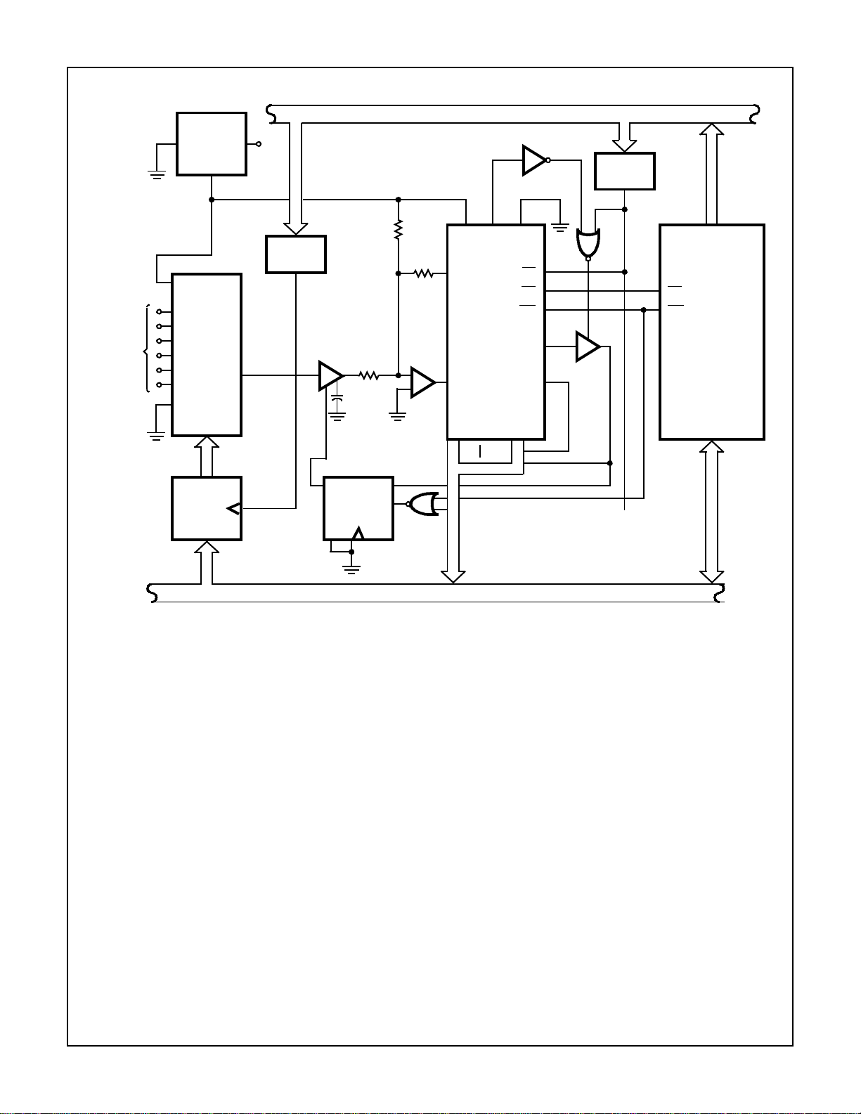
Functional Block Diagram
V
REF
AGND
Y
DGND
+
-
V
DAC
R-1.85R
PROM
LATCH
V
IN
R
IN
COMP
+
C
AZ
-
CONTROL LOGIC
ADDER
ACCCUM
SAR
OSC1 OSC2
LATCH
WR
EOC
THREE-STATE
OUTPUTS
CSRD
0
OVR
D
(MSB)
11
D
(LSB)
0
BUSA
6-2
Page 3
ICL7112
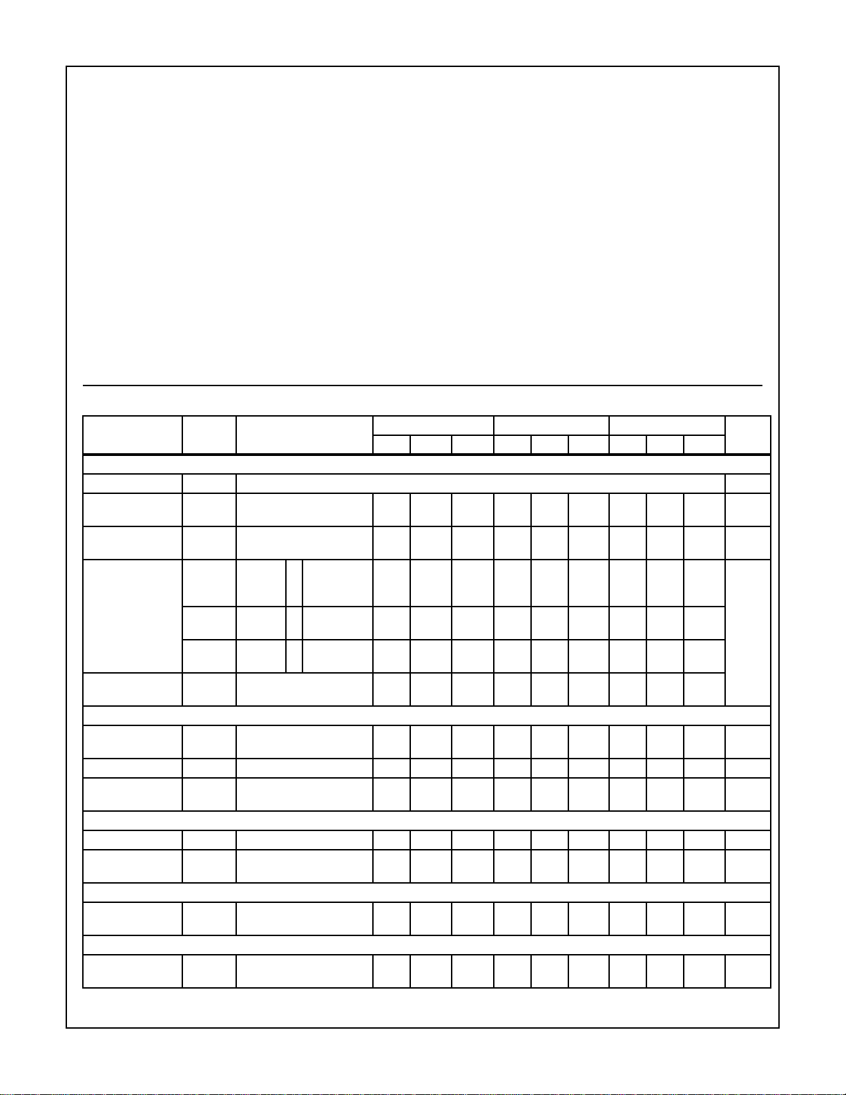
Absolute Maximum Ratings T
Supply Voltage (V+ to DGND) . . . . . . . . . . . . . . . . . . -0.3V to +6.5V
Supply Voltage (V
V
, VIN to DGND . . . . . . . . . . . . . . . . . . . . . . . . . . . . . . . . . ±25V
REF
AGND to DGND . . . . . . . . . . . . . . . . . . . . . . . . . . . . . . . . +1V to -1V
V
, VIN, AGND Current . . . . . . . . . . . . . . . . . . . . . . . . . . . . 25mA
REF
Digital I/O Pin Voltages. . . . . . . . . . . . . . . . . . . . . -0.3V to V+ +0.3V
PROG to DGND Voltage . . . . . . . . . . . . . . . . . . . . V
-
to DGND). . . . . . . . . . . . . . . . . . . +0.3V to -6.5V
=25oC Thermal Information
A
Thermal Resistance (Typical, Note 1) θ
CERDIP Package . . . . . . . . . . . . . . . . ___ ___
Maximum Power Dissipation (Note 2) . . . . . . . . . . . . . . . . . . 500mW
Derate above 70
o
C at 10mW/oC
Maximum Junction Temperature (Ceramic Package) . . . . . . . . 175
-
to (V+ +0.3V)
Maximum Storage Temperature Range . . . . . . . . . . -65
Maximum Lead Temperature (Soldering 10s). . . . . . . . . . . . . 300
(oC/W) θJC (oC/W)
JA
o
C to 150oC
o
o
Operating Conditions
ICL7112XCXX. . . . . . . . . . . . . . . . . . . . . . . . . . . . . . . . . . . 0 to 70
ICL7112XIXX . . . . . . . . . . . . . . . . . . . . . . . . . . . . . . . . . -25 to 70
ICL7112XMXX . . . . . . . . . . . . . . . . . . . . . . . . . . . . . . . -55 to 125
CAUTION: Stresses above those listed in “Absolute Maximum Ratings” may cause permanent damage to the device. This is a stress only rating and operation
of the device at these or any other conditions above those indicated in the operational sections of this specification is not implied.
NOTES:
is measured with the component mounted on an evaluation PC board in free air.
1. θ
JA
2. All voltages with respect to DGND, unless otherwise noted.
3. Assumes all leads soldered or welded to printed circuit board.
Electrical Specifications Test Conditions: V+ = +5V, V- = -5V, V
PARAMETER SYMBOL
ACCURACY
Resolution RES 12 Bits
Resolution with No
Missing Codes
Integral Linearity
Error
Unadjusted Full
Scale Error
RES
Notes 4, 5, 6 R
(NMC)
I
LE
Notes 4, 5 R
FSE Adjust-
able to
Zero
Zero Error ZE Notes 4, 5 R
ANALOG INPUT
Analog Input
Range
Input Resistance R
Temperature
Coefficient of R
V
IN
IN
Notes 5, 8 4 - 9 4 - 9 4 - 9 kΩ
TC (RIN)T
IN
REFERENCE INPUT
Analog Reference V
Reference
Resistance
R
REF
REF
POWER SUPPLY SENSITIVITY
Power Supply
PSRR V
+
Rejection Ration
LOGIC INPUT
Low State
V
IL
Input Voltage
TEST
CONDITIONS
T
-T
MIN
MAX
T
-T
MIN
MAX
CR
T
MIN TMAX
IR
T
-T
MIN
MAX
MR
T
-T
MIN
MAX
T
-T
MIN
MAX
-T
MIN
MAX
, V- = 4.5 -5.5V RM
T
-T
MIN
MAX
T
-T
MIN
MAX
11
M
10
--±0.024
M
--±0.10
M
--±0.10
M
--±0.10
M
--±1
M
0 -10.30-10.30-10.3V
- -300 - - -300 - - -300 - ppm/oC
- -10.0 - - -10.0 - - -10.0 - V
-5 - -5--5-kΩ
- ±0.5 ±1
--0.8--0.8--0.8V
= -10V, TA = 25oC, f
REF
= 500kHz, Unless Otherwise Noted
CLK
JKL
UNITSMIN TYP MAX MIN TYP MAX MIN TYP MAX
--1211--1212--
±0.030
±0.12
±0.13
±0.14
±1.5
±2
--±0.012
±0.020
--±0.08
±0.10
--±0.08
±0.11
--±0.08
±0.12
--±1
±1.5
- ±0.5 ±1
±2
--±0.012
±0.020
--±0.08
±0.10
--±0.08
±0.11
--±0.08
±0.12
--±1
±1.5
- ±0.5 ±1±2LSB
Bits
%FSR
%FSR
C
C
6-3
Page 4
ICL7112
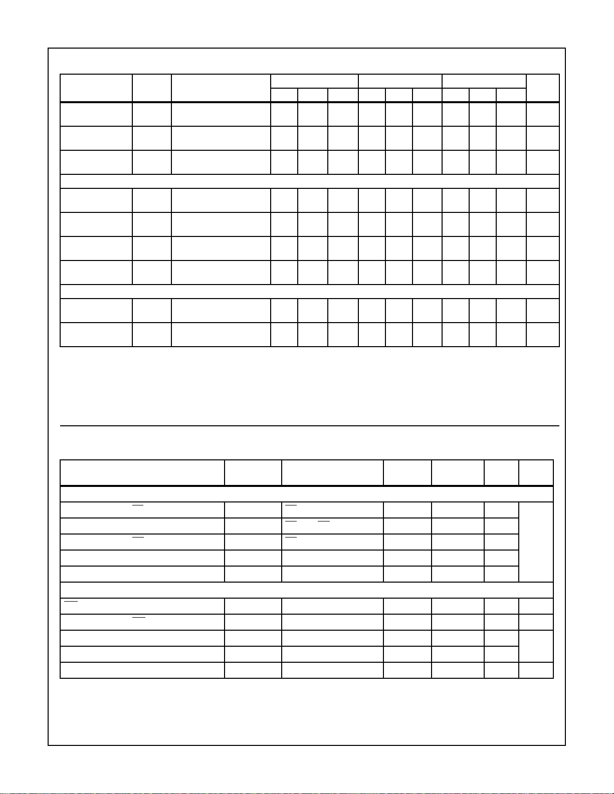
Electrical Specifications Test Conditions: V+ = +5V, V- = -5V, V
TEST
PARAMETER SYMBOL
High State
V
IH
CONDITIONS
T
MIN
-T
MAX
2.4 - - 2.4 - - 2.4 - - V
= -10V, TA = 25oC, f
REF
JKL
Input Voltage
Logic Input
I
LIH
0 < VIN < V
+
- 110-110-110µA
Current
Logic Input
C
IN
- 15 - -15 - -15 - pF
Capacitance
LOGIC OUTPUT
Low State Output
Voltage
High State Output
Voltage
Three-State Output
Current
Logic Output
Capacitance
V
V
I
C
OL
OH
OX
OUT
= 1.6mA
OUT
I
OUT
0 < V
= -200µA
< V
OUT
T
T
+
MIN
MIN
-T
-T
MAX
MAX
Three-State - 15 - - 15 - - 15 - pF
--0.4--0.4--0.4V
2.8 - - 2.8 - - 2.8 - - V
-1 - -1--1-µA
I
POWER REQUIREMENTS
Supply Voltage
Range
Supply Current,
I+, I-
V
SUPPLY
I
SUPPLY
Functional Operation Only ±4.5 - ±6.0 ±4.5 - ±6.0 ±4.5 - ±6.0 V
T
MIN
-T
R
MAX
-246-246-246mA
M
NOTES:
4. Full scale range (FSR) is 10V (reference adjusted).
5. Assume all leads are soldered or welded to printed circuit board.
6. “J” and “K” versions not production tested. Guaranteed by Integral Linearity Test.
7. Typical values are not tested, for reference only.
8. Not production tested. Guaranteed by design.
= 500kHz, Unless Otherwise Noted
CLK
UNITSMIN TYP MAX MIN TYP MAX MIN TYP MAX
AC Electrical Specifications Test Conditions V + = +5V, V- = -5V, T
derived from extensive characterization testing. Parameters are not production tested
PARAMETER SYMBOL
READ CYCLE TIMING
Propagation Delay CS
Propagation Delay A0 to Data t
Propagation Delay RD
Propagation Delay Data to Three-State t
Propagation Delay EOC High to Data t
to Date t
to Data t
cd
ad
rd
rx
ed
WRITE CYCLE TIMING
WR
Low Time t
Propagation Delay WR Low to EOC Low t
EOC High Time t
Conversion Time t
Clock Frequency Range f
wr
we
eo
conv
CLK
NOTE:
9. All typical values have been characterized, but are not tested.
RD Low, A0 Valid - - 200
CS Low, RD Low - - 200
CS Low, A0 Valid - - 200
Wait Mode 1 - 2
Free Run Mode 0.5 - 1.5 1/f
Functional Operation Only - 500 - kHz
TEST
CONDITIONS MIN TYP MAX UNITS
= 25oC, f
A
= 500kHz, unless otherwise noted. Data
CLK
--150
--200
150 - - ns
--20
ns
CLK
6-4
Page 5
ICL7112
Pin Descriptions
PIN NO. NAME DESCRIPTION
1 No connection.
2AGND
3CS
4RD
5A
0
6 BUS Bus select (low = outputs enabled by A
7 DGND Digital GrouND return.
8D
9D
10 D
11 D
12 D
13 D
14 D
15 D
16 D
17 D
18 D
11
10
9
8
7
6
5
4
3
2
1
19 D0 Bit 0 (least significant bit).
20 No connection.
21 No connection.
22 No connection.
23 No connection.
24 No connection.
25 EOC End of conversion flag (low = busy, high = conversion complete).
26 OVR OVerRange flag (valid at end of conversion when output code exceeds full-scale;
27 V
+
28 PROG Used for programming only. Must tie to V
29 TEST Used for programming only. Must tie to V
30 OSC1 Oscillator inverter input.
31 OSC2 Oscillator inverter output.
32 TEST Must tie to V
33 WR
34 C
35 V
AZ
-
36 COMP Used in test, tie to V
37 V
38 V
IN
REF
39 AGND
40 No connection
NOTE: The voltage of CAZ is driven; NEVER connect directly to ground.
FORCE input for analog ground.
f
Chip Select enables reading and writing (active low).
ReaD (active low).
Byte select (low = D0 -D7, high = D8 -D11, OVR).
Bit 11 (most significant bit).
Bit 10
Bit 9
Bit 8
Bit 7
Bit 6
Bit 5
Bit 4
Bit 3
Bit 2
Bit 1
three-state output enabled with high byte).
Positive power supply input.
+
for normal operation.
WRite pulse input (low starts new conversion).
Auto-zero capacitor connection (Note).
Negative power supply input.
SENSE line for input voltage.
SENSE line for reference input.
SENSE line for analog ground.
s
, high = all outputs enabled together).
0
High Byte
Output
Data
Bits
(High =True)
Low Byte
+
for normal operation.
+
for normal operation.
-
.
6-5
Page 6

Timing Diagrams
CS
WR
EOC
D0 - D
EOC
CS
A
0
RD
13
= DON’T CARE
ICL7112
t
CD
VALID
t
AD
t
RD
t
ED
= DON’T CARE
FIGURE 1. READ CYCLE TIMING
t
WR
FIGURE 2. WRITE CYCLE TIMING
VALID
t
WE
t
RX
t
CONV
t
EO
TABLE 2: I/O CONTROL
CS
WR RD A0BUS FUNCTION
0 0 x x x Initiates a conversion.
1 x x x x Disables all chip commands.
0 x 0 0 0 Low byte is enabled.
0 x 0 1 0 High byte is enabled.
0 x 0 x 1 Low and High bytes enabled togeth-
x x 1 x x Disables outputs (high-impedance).
TABLE 3: TRANSFER FUNCTION
INPUT VOLTAGE EXPECTED OUTPUT CODE
= -10.0V OVR MSB LSB
V
REF
0
+0.00244
+0.30029 0 0 0000111101 1
+4.99756
+5.00000
+9.99512
+9.99756
+10.00000
+10.00244
+10.29000 1 0 0000111101 1
er.
0
0
0
0
0
0
1
1
0
0
0
1
1
1
0
0
0000000000
0000000000
1111111111
0000000000
1111111111
1111111111
0000000000
0000000000
0
1
1
0
0
1
0
1
Detailed Description
The ICL7112 is basically a successive approximation A/D
converter with an internal structure much more complex than
a standard SAR-type converter. The Functional Block Diagram shows the functional diagram of the ICL7112 12-bit
A/D converter. The additional circuitry incorporated into the
ICL7112 is used to perform error correction and to maintain
the operating speed in the 40µs range.
The internal DAC of the ICL7112 is designed around a radix
of 1.85, rather than the traditional 2.00. This radix gives each
bit of the DAC a weight of approximately 54% of the previous
bit. The result is a usable range that extends to 3% beyond
the full-scale input of the A/D. The actual value of each bit is
measured and stored in the on-chip PROM. The absolute
value of each bit weight then becomes relatively unimportant
because of the error correction action of the ICL7112.
The output of the high-speed auto-zeroed comparator is fed
to the data input of a successive approximation register
(SAR). This register is uniquely designed for the ICL7112 in
that it tests bit pairs instead of individual bits in the manner of
a standard SAR. At the beginning of the conversion cycle,
the SAR turns on the MSB (D
The sequence continues for each bit pair, B
) and the MSB 4-bit (D7).
11
and B
X
x-4
, until
only the four LSBs remain. The sequence concludes by testing the four LSBs individually.
The SAR output is fed to the DAC register and to the preprogrammed PROM where it acts as PROM address. PROM
data is fed to a full-adder/accumulator where the decoded
results from each successive phase of the conversion are
summed with the previous results. After 20 clock cycles, the
accumulator contains the final binary data which is latched
and sent to the three-state output buffers. The accuracy of
the A/D converter depends primarily upon the accuracy of
the data that has been programmed into the PROM during
6-6
Page 7

ICL7112
the final test portion of the manufacturing process.
The error correcting algorithm built into the ICL7112 reduces
the initial accuracy requirements of the DAC. The overlap in
the testing of bit pairs reduces the accuracy requirements on
the comparator which has been optimized for speed. Since
the comparator is auto-zeroed, no external adjustment is
required to get ZERO code for ZERO input voltage.
Twenty clock cycles are required for the complete 12-bit conversion. The auto-zero circuitry associated with the comparator is employed during the last three clock cycles of the
conversion to cancel the effect of offset voltage. Also during
this time, the SAR and accumulator are reset in preparation
for the start of the next conversion.
The overflow output of the full-adder is also the OVer Range
(OVR) output of the ICL7112. Unlike standard SAR type A/D
converters, the ICL7112 has the capability of providing valid
usable data for inputs that exceed the fullscale range by as
much as 3%.
Optimizing System Performance
When using A/D converters with 12 or more bits of resolution, special attention must be paid to grounding and the
elimination of potential ground loops. A ground loop can be
formed by allowing the return current from the lCL7112’s
DAC to flow through traces that are common to other analog
circuitry. If care is not taken, this current can generate small
unwanted voltages that add to or detract from the reference
or input voltages of the A/D converter.
Figure 3 and Figure 4 show two different grounding techniques. Although the difference between the two circuits may
not be readily apparent, the circuit of Figure 3 is very likely to
have significant ground loop errors which the circuit of Figure 4 avoids. In Figure 3, the supply currents for analog
ground, digital ground, and the reference voltage all flow
through a lead, common to the input. This will generate a DC
offset voltage due to the currents flowing in the resistance of
the common lead. This offset voltage will vary with the input
voltage and with the digital output. Even the auto-zero loop
of the ICL7112 cannot remove this error.
Figure 4 shows a much better arrangement. The ground and
reference currents do not flow through the input common
lead, eliminating any error voltages. Note that the supply
currents and any other analog system currents must also be
returned carefully to analog ground. The clamp diodes will
protect the ICL7112 against signals which could result from
separate analog and digital grounds. The absolute maximum
voltage rating between AGND and DGND is ±1.0V. The two
inverse-parallel diodes clamp this voltage to less than ±0.7V.
Input Warning
As with any CMOS integrated circuit, no input voltages
should be applied to the lCL7112 until the ±5V power supplies have stabilized.
Interfacing To Digital Systems
The_ICL7112 provides three-state data output buffers, CS,
RD
, WR, and bus select inputs (A0 and BUS) for interfacing
to a wide variety of microcomputers and digital systems. The
I/O Control Truth Table shows the functions of the digital
control lines. The BUS select and A
enable the output data onto either 8-bit or 16-bit data buses.
A conversion is initiated by a WR
(pin 3) is low. Data is enabled on the bus when the chip is
selected and RD
(pin 4) is low.
Figure 5 illustrates a typical interface to an 8-bit microcomputer. The “Start and Wait” operation requires the fewest
external components and is initiated by a low level on the
WR
input to the ICL7112 after the I/O or memory mapped
address decoder has brought the CS
ing a delay or utility routine for a period of time greater than
the conversion time of the ICL7112, the processor issues
two consecutive bus addresses to read output data into two
bytes of memory. A low level on A
high level enables the MSBs.
lines are provided to
0
pulse (pin 33) when CS
input low. After execut-
enables the LSBs, and a
0
V
IN +
SOURCE -
V
REF -
SOURCE +
FIGURE 3. IMPROPER GROUNDING TECHNIQUE WILL CAUSE GROUND LOOP ERRORS
V
IN
ICL7112
V
REF
AGND
DGND
6-7
Page 8

ICL7112
V
IN +
SOURCE -
V
REF -
SOURCE +
V
IN
ICL7112
V
REF
AGND
DGND
FIGURE 4. RECOMMENDED GROUNDING TECHNIQUE TO ELIMINATE GROUND LOOP ERRORS
ADDRESS BUS
A
0
A
0
ICL7112
ADDRESS
DECODE
CS
RD
WR
BUS
OVR
RD
WR
A0 - A
µP
N
CS
OVR
- D
D
8
11
7
WAIT
WR
CS
A
0
RD
START
CONVERSION
D0 - D
FIGURE 5. “START AND WAIT” OPERATION
By adding a three-state buffer and two control gates, the
End-of-Conversion (EOC) output can be used to control a
“Start and Poll” interface (Figure 6). In this mode, the A
CS
lines connect the EOC output to the data bus along with
the most significant byte of data. After pulsing the WR
and
0
line to
initiate a conversion, the microprocessor continually reads
the most significant byte until it detects a high level on the
EOC bit. The “Start and Poll” interface increases data
throughput compared with the “Start and Wait” method by
eliminating delays between the conversion termination and
- D
D
0
7
DATA BUS
READ
LOW BYTE
READ
HIGH BYTE
the microprocessor read operation.
Other interface configurations can be used to increase data
throughput without monopolizing the microprocessor during
waiting or polling operations by using the EOC line as an
interrupt generator as shown in Figure 7. After the conversion cycle is initiated, the microprocessor can continue to
execute routines that are independent of the A/D converter
until the converter’s output register actually holds valid data.
For fastest data throughput, the ICL7112 can be connected
directly to the data bus but controlled by way of a Direct
6-8
Page 9

ICL7112
Memory Access (DMA) controller as shown in Figure 8.
Applications
Figure 9 shows a typical application of the ICL7112 12- bit
A/D converter. A bipolar input voltage range of +10V to -10V
is the result of using the current through R
scale offset on the input amplifier (A
swings from 0V to -1 0V. The overall gain of the A/D is varied
by adjusting the 100Ω trim resistor, R
5
automatically zeroed every conversion, the system gain and
offset stability will be superb as long as a reference with a
tempco of 1ppm/
o
C and stable external resistors are used.
If is important to note that since the 7112’s DAC current
flows in A
, the amplifier should be a wideband (GBW >
1
20MHz) type to minimize errors.
The clock for the ICL7112 is taken from whatever system
clock is available and divided down to the level for a conversion time of 40µs. Output data is controlled by the BUS and
A
inputs. Here they are set for 8-bit bus operation with BUS
0
grounded and A
under the control of the address decode
0
section of the external system.
Because the ICL7112’s internal accumulator generates
accurate output data for input signals as much as 3% greater
than full-scale, and because the converter’s OVR output
flags overrange inputs, a simple microprocessor routine can
be employed to precisely measure and correct for system
gain and offset errors. Figure 10 shows a typical data acquisition system that uses a 10V reference, input signal multiplexer, and input signal Track/Hold amplifier. Two of the
multiplexer’s input channels are dedicated to sampling the
system analog ground and reference voltage. Here, as in
Figure 9, bipolar operation is accommodated by an offset
resistor between the reference voltage and the summing
junction of A
. A flip-flop in IC3 sets 1C2’s Track/Hold input
1
after the microprocessor has initiated a WR command, and
resets when EOC goes high at the end of the conversion.
The first step in the system calibration routine is to select the
multiplexer channel that is connected to system analog
ground and initiate a conversion cycle for the ICL7112. The
results represent the system offset error which comes from
the sum of the offsets from IC
, IC2, and A1. Next the chan-
1
nel connected to the reference voltage is selected and measured. These results, minus the system offset error,
represent the system full-scale range. A gain error correction
factor can be derived from this data. Since the lCL7112 provides valid data for inputs that exceed full-scale by as much
as 3%, the OVR output can be thought of as a valid 13th
data bit. Whenever the OVR bit is high, however, the total
12-bit result should be checked to ensure that it falls within
100% and 103% of full-scale. Data beyond 103% of fullscale should be discarded.
to force a 1/2
2
). The output of A
1
. Since the ICL7112 is
1
Clock Considerations
The ICL7112 provides an internal inverter which is brought
out to pins OSC1 and OSC2, for crystal or ceramic resonator
oscillator operation. The clock frequency is calculated from:
=
20
------ ----------- -
t
CONV
f
CLK
6-9
Page 10

()
ICL7112
ADDRESS BUS
A
0
WR
CS
EOC
D0 - D
A
ICL7112
D
8
7
0
- D
WR
RD
A0 - A
µP
- D
D
0
N
CS
7
ADDRESS
DECODE
WR
CS
RD
EOC
BUS
OVR
11
1/4 74125
DATA BUS
(B)
END OF
CONVERSION
A
RD
0
START
CONVERSION
POLL
READ
HIGH BYTE
READ
HIGH BYTE
READ
LOW BYTE
FIGURE 6. START AND POLL” OPERATION
6-10
Page 11

ICL7112
ADDRESS BUS
A
0
WR
D0 - D
A
0
ICL7112
- D
D
8
7
INTERRUPT
WR
EOC
BUS
OVR
11
CS
RD
ADDRESS
DECODE
DATA BUS
RD
WR
INT
A0 - A
µP
- D
D
0
N
7
CS
EOC
A
RD
0
START
CONVERSION
READ
LOW BYTE
READ
HIGH BYTE
FIGURE 7. USING EOC AS AN INTERRUPT
6-11
Page 12

ICL7112
ADDRESS BUS
A
0
EOC
D0 - D
A
0
ICL7112
D
7
DRQ
DACK
A0 - A
N
N
DMA
11
CS
WR
EOC
RD
CS
CONTROLLER
BUS
OVR
- D
8
11
D
- D
0
7
DATA BUS
DACK
N
A
0
READ
LOW BYTE
END OF
CONVERSION
READ
HIGH BYTE
START
CONVERSION
FIGURE 8. DATA TO MEMORY VIA DMA CONTROLLER
6-12
Page 13

10V
REFERENCE
INPUT VOLTAGE
+10V TO -10V
HI
LO
R
R
1
100k
ICL7112
+5V
28 32 29 27 500KHz
OSC
EOC
DATA
OUT
WR
RD
CS
A
+
30
DIVIDER
25
26
HIGH
BYTE
13
14
LOW BYTE
21
33
4
3
ADDRESS
5
0
DECODE
PINS 1, 20, 21, 22, 23, 24, 40
NO CONNECTIONS
SYSTEM
CLOCK
8-BIT
DATA BUS
4
R
5
100K
R
R
2
A
2
-
+
A
2
-
+
DIODES
1N914
3
50k
0.22µF
100k
PROG TEST V
36
V
REF
37
V
IN
34
CAZ
AGND
39
AGND
2
COMP
TEST
ICL7112
V+DGND BUS
36 35 7 6
DIGITAL
-5V
GROUND
FIGURE 9. TYPICAL APPLICATION WITH BIPOLAR INPUT RANGE, FORCED GROUND, AND 10V ULTRA STABLE REFERENCE
6-13
Page 14
ADDRESS BUS
ANALOG
INPUTS
REFERENCE
10V
I
S
IC
1
IH5108
OUT
I
R
- A
A
0
2
DATA
LATCH
V
CC
ADDRESS
DECODE
IC 2
LF398
Q
1/2 4013
D
ADDRESS
DECODE
V
V
REF
S
0
ICL7112
BUSA
A0 - A
N
CS
RD
WR
RD
WR
µP
EOC
10k
+
V
R
D8 - D13D0 - D
OVR
7
1/2
74125
D
- D
0
7
R
IC
3
S
DATA BUS
FIGURE 10. MULTI-CHANNEL DATA ACQUISITION SYSTEM WITH ZERO AND REFERENCE LINES BROUGHT TO MULTIPLEXER
FOR SYSTEM GAIN AND OFFSET ERROR CORRECTION
6-14
 Loading...