Intersil Corporation ICL232CBE, ICL232CPE, ICL232lBE, ICL232lPE, ICL232MJE Datasheet

TM
ICL232
itle
L23
b-
t
V
w-
d,
al
-
2
ns-
t-
/Rec
er)
utho
)
ey-
rds
ter-
rpo-
ion)
re-
r()
OCI
O
f-
rk
ge-
de
se-
t-
es
OCEW
f-
June 2001
+5V Powered, Dual RS-232 Transmitter/Receiver
Features
• Meets All RS-232C and V.28 Specifications
• Requires Only Single +5V Power Supply
• Onboard Voltage Doubler/Inverter
• Low Power Consumption
•2Drivers
- ±9V Output Swing for +5V lnput
-300Ω Power-off Source Impedance
- Output Current Limiting
- TTL/CMOS Compatible
-30V/µs Maximum Slew Rate
• 2 Receivers
- ±30V Input Voltage Range
-3kΩ to 7kΩ Input I mpedance
- 0.5V Hysteresis to Improve Noise Rejection
• All Critical Parameters are Guaranteed Over the Entire
Commercial, Industrial and Military Temperature Ranges
Applications
• Any System Requiring RS-232 Communications Port
- Computer - Portable and Mainframe
- Peripheral - Printers and Terminals
- Portable Instrumentation
- Modems
• Dataloggers
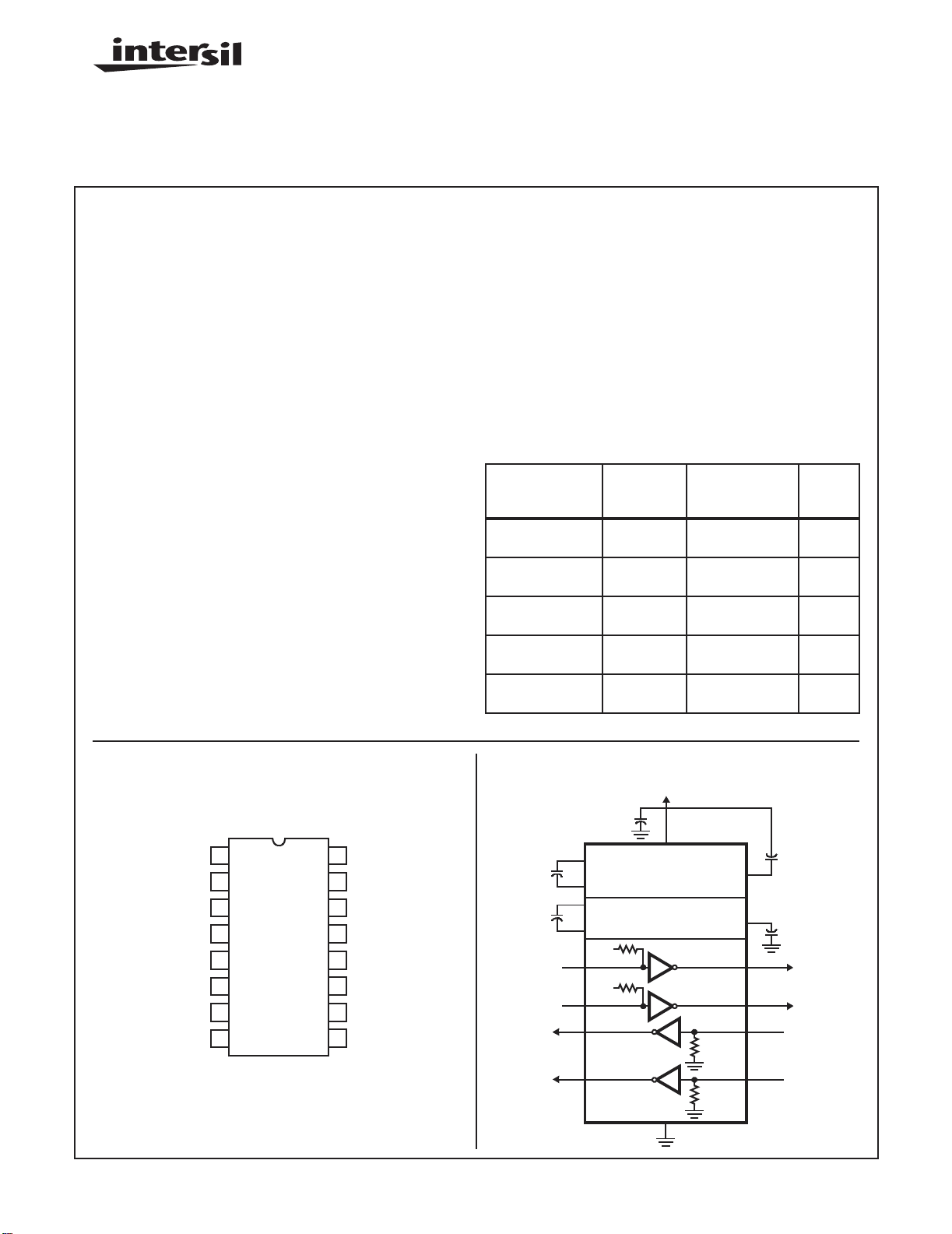
Pinout
ICL232 (PDIP, CERDIP, SOIC)
TOP VIEW
C1+
1
V+
2
C1-
3
4
C2+
5
C2-
6
V-
T2
7
OUT
R2
8
IN
16
V
CC
15
GND
14
T1
OUT
13
R1
IN
R1
12
OUT
T1
11
IN
T2
10
IN
9
R2
OUT
Description
The ICL232 is a dual RS-232 transmitter/receiver interface
circuit that meets all ElA RS-232C and V.28 specifications. It
requires a single +5V power supply, and features two
onboard charge pump voltage converters which generate
+10V and -10V supplies from the 5V supply.
The drivers feature true TTL/CMOS input compatibility, slewrate-limited output, and 300Ω power-off source impedance.
The receiverscan handle up to +30V,andhavea3kΩ to 7kΩ
input impedance. The receivers also have hysteresis to
improve noise rejection.
Ordering Information
TEMP.
PART NUMBER
ICL232CPE 0 to 70 16 Ld PDIP E16.3
ICL232CBE 0 to 70 16 Ld SOIC M16.3
ICL232lPE -40 to 85 16 Ld PDIP E16.3
ICL232lBE -40 to 85 16 Ld SOIC M16.3
ICL232MJE -55 to 125 16 Ld CERDIP F16.3
RANGE (oC) PACKAGE
PKG.
NO.
Functional Diagram
+5V
+
R1
R2
1µF
1µF
T1
T2
OUT
OUT
1.0µF
1
C1+
+
3
VOLTAGE INVERTER
C1-
4
C2+
+
5
VOLTAGE INVERTER
C2-
+5V
400kΩ
11
IN
400kΩ
10
IN
16
V
CC
+5V TO 10V
+10V TO -10V
T1
T2+5V
R1
R2
5kΩ
5kΩ
V+
1µF
+
2
6
V-
1µF
+
14
T1
OUT
7
T2
OUT
1312
R1
IN
89
R2
IN
1-888-INTERSIL or 321-724-7143
CAUTION: These devices are sensitive to electrostatic discharge; follow proper IC Handling Procedures.
| Intersiland Design is atrademarkof IntersilAmericasInc. | Copyright ©Intersil Americas Inc. 2001
1
15
File Number 3020.6

ICL232
Absolute M axi m um Ratings Thermal Information
VCCtoGround......................(GND-0.3V)<VCC<6V
V+toGround....................... (V
-0.3V)<V+<12V
CC
V-toGround.......................-12V<V-<(GND+0.3V)
Input Voltages
T1
,T2IN....................(V--0.3V)<VIN<(V++0.3V)
IN
R1
,R2IN......................................±30V
IN
OutputVoltages
T1
,T2
OUT
R1
,R2
OUT
Short Circuit Duration
T1
,T2
OUT
R1
,R2
OUT
............(V--0.3V)<V
OUT
.........(GND-0.3V)<V
OUT
..............................Continuous
OUT
..............................Continuous
OUT
RXOUT
TXOUT
<(VCC+0.3V)
<(V++0.3V)
Operating Conditions
Temperature Ranges
ICL232C...................................0
ICL232I..................................-40
ICL232M................................-55
CAUTION: Stresses above those listed in “Absolute Maximum Ratings” may cause permanent damage to the device. This is a stress only rating and operation
of the device at these or any other conditions above those indicated in the operational sections of this specification is not implied.
NOTE:
is measured with the componentmountedon an evaluation PC board in free air.
1. θ
JA
o
Cto70oC
o
Cto85oC
o
Cto125oC
Thermal Resistance (Typical, Note 1) θ
CERDIPPackage................ 80 18
(oC/W) θJC(oC/W)
JA
PDIPPackage................... 100 N/A
SOICPackage................... 100 N/A
MaximumJunction Temperature
PlasticPackages.................................150
CeramicPackage................................175
MaximumStorageTemperatureRange..........-65
o
Cto150oC
MaximumLeadTemperature(Soldering10s).............300
o
o
o
C
C
C
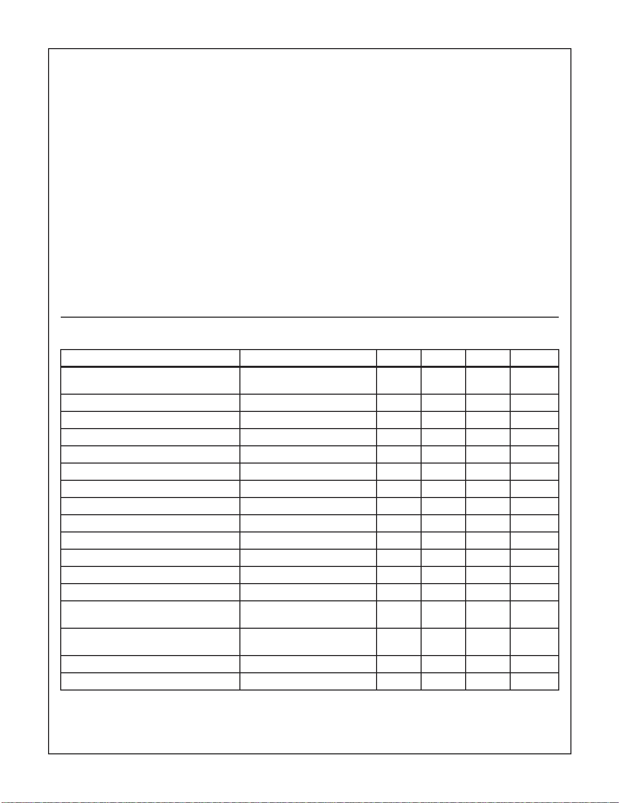
Electrical Specifications Test Conditions : V
UnlessOtherwise Specified
PARAMETER TEST CONDITIONS M IN TYP MAX UNITS
Transmitter Output Voltage Swing, T
Power Supply Current,I
T
, InputLogic Low, V
IN
T
, InputLogic High, V
IN
LogicPullup Current, I
CC
lL
lH
P
RS-232 Input VoltageRange, V
ReceiverInput Impedance, R
ReceiverInput Low Threshold,V
ReceiverInput H igh Threshold, V
ReceiverInput Hysteresis,V
OUT
IN
IN
(H-L) VCC=5V,TA=25oC0.81.2-V
lN
(L-H) VCC=5V,TA=25oC-1.72.4V
IN
HYST
TTL/CMOS Receiver Output Voltage Low, V
TTL/CMOSReceiver Output Voltage High, V
Propagation Delay, t
PD
Instantaneous Slew Rate, S R C
Transition Region Slew Rate, SR
T
T1
to Ground
Outputs Unloaded, TA=25oC-510mA
T1IN,T2IN= 0V - 15 200 µA
VIN= ±3V 3.0 5.0 7.0 kΩ
OLIOUT
OHIOUT
RS-232 to TTL - 0.5 - µs
(Notes 2, 3)
RL=3kΩ,CL= 2500pF Measured
from +3V to -3V or -3V to +3V
=+5V ±10%, TA= Operating Temperature Range. Test Circuit as in Figure 8
CC
OUT
andT2
Loaded with 3kΩ
OUT
±5 ±9 ±10 V
--0.8V
2.0 - - V
-30-+30V
0.2 0.5 1.0 V
= 3.2mA - 0.1 0.4 V
= -1.0mA 3.5 4.6 - V
=10pF,RL=3kΩ,TA=25oC
L
--30V/µs
-3-V/µs
Output Resistance, R
OUT
RS-232 Output Short Circuit Current, I
NOTES:
2. Guaranteed by design.
3. See Figure 4 for definition.
SC
VCC=V+=V-=0V,V
T1
OUT
or T2
Shorted to GND - ±10 - mA
OUT
2
= ±2V 300 - - Ω
OUT
 Loading...