ICL232
August 1997
+5V Powered, Dual RS-232 Transmitter/Receiver
Features
• Meets All RS-232C and V.28 Specifications
• Requires Only Single +5V Power Supply
• Onboard Voltage Doubler/Inverter
• Low Power Consumption
• 2 Drivers
- ±9V Output Swing for +5V lnput
- 300Ω Power-off Source Impedance
- Output Current Limiting
- TTL/CMOS Compatible
- 30V/µs Maximum Slew Rate
• 2 Receivers
- ±30V Input Voltage Range
-3kΩ to 7kΩ Input Impedance
- 0.5V Hysteresis to Improve Noise Rejection
• All Critical Parameters are Guaranteed Over the Entire
Commercial, Industrial and Military Temperature Ranges
Applications
• Any System Requiring RS-232 Communications Port
- Computer - Portable and Mainframe
- Peripheral - Printers and Terminals
- Portable Instrumentation
- Modems
• Dataloggers
Description
The ICL232 is a dual RS-232 transmitter/receiver interface
circuit that meets all ElA RS-232C and V.28 specifications. It
requires a single +5V power supply, and features two
onboard charge pump voltage converters which generate
+10V and -10V supplies from the 5V supply.
The drivers feature true TTL/CMOS input compatibility, slewrate-limited output, and 300Ω power-off source impedance.
The receivers can handle up to +30V, and ha v e a 3kΩ to 7kΩ
input impedance. The receivers also have hysteresis to
improve noise rejection.
Ordering Information
TEMP.
PART NUMBER
RANGE (oC) PACKAGE
ICL232CPE 0 to 70 16 Ld PDIP E16.3
ICL232CBE 0 to 70 16 Ld SOIC M16.3
ICL232lPE -40 to 85 16 Ld PDIP E16.3
ICL232lJE -40 to 85 16 Ld CERDIP F16.3
ICL232lBE -40 to 85 16 Ld SOIC M16.3
ICL232MJE -55 to 125 16 Ld CERDIP F16.3
PKG.
NO.
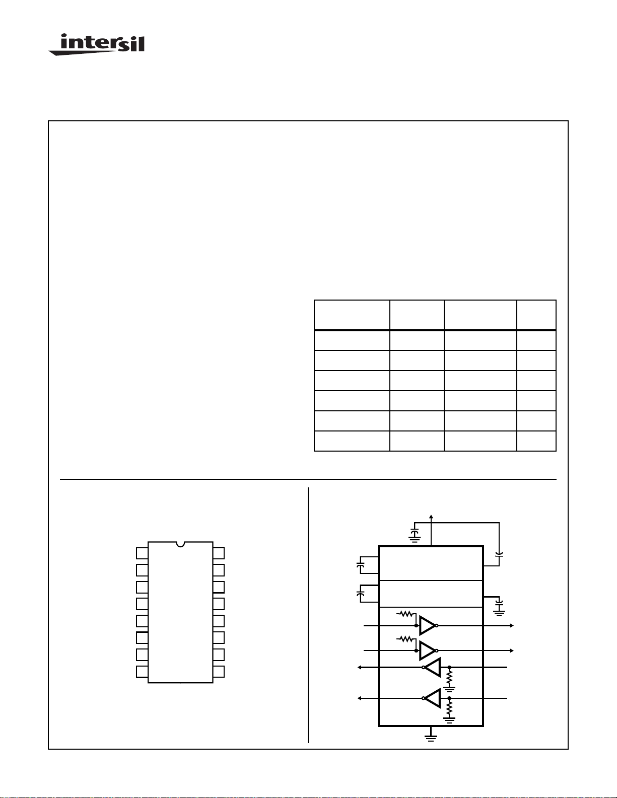
Pinout
Functional Diagram
ICL232 (PDIP, CERDIP, SOIC)
TOP VIEW
C1+
1
V+
2
C1-
3
C2+
4
C2-
5
6
V-
T2
7
OUT
R2
8
IN
CAUTION: These devices are sensitive to electrostatic discharge; follow proper IC Handling Procedures.
http://www.intersil.com or 407-727-9207
| Copyright © Intersil Corporation 1999
16
V
CC
15
GND
14
T1
OUT
13
R1
IN
R1
12
OUT
T1
11
IN
T2
10
IN
9
R2
OUT
R1
R2
1µF
1µF
T1
T2
OUT
OUT
IN
IN
8-49
+5V
+
1.0µF
1
C1+
+
3
VOLTAGE INVERTER
C1-
4
C2+
+
5
VOLTAGE INVERTER
C2-
+5V
400kΩ
11
+5V
400kΩ
10
16
V
CC
+5V TO 10V
+10V TO -10V
T1
T2
R1
R2
15
5kΩ
5kΩ
V+
1µF
+
2
6
V-
1µF
+
14
7
1312
89
R1
R2
T1
T2
OUT
OUT
IN
IN
File Number 3020.5

ICL232
Absolute Maximum Ratings Thermal Information
VCC to Ground . . . . . . . . . . . . . . . . . . . . . .(GND -0.3V) < VCC < 6V
V+ to Ground . . . . . . . . . . . . . . . . . . . . . . . (VCC -0.3V) < V+ < 12V
V- to Ground. . . . . . . . . . . . . . . . . . . . . . . -12V < V- < (GND +0.3V)
Input Voltages
T1IN, T2IN. . . . . . . . . . . . . . . . . . . . (V- -0.3V) < VIN < (V+ +0.3V)
R1IN, R2IN . . . . . . . . . . . . . . . . . . . . . . . . . . . . . . . . . . . . . . ±30V
Output Voltages
T1
, T2
R1
OUT
OUT
. . . . . . . . . . . . (V- -0.3V) < V
OUT
, R2
. . . . . . . . .(GND -0.3V) < V
OUT
RXOUT
< (V+ +0.3V)
TXOUT
< (VCC +0.3V)
Short Circuit Duration
T1
, T2
. . . . . . . . . . . . . . . . . . . . . . . . . . . . . . Continuous
OUT
, R2
. . . . . . . . . . . . . . . . . . . . . . . . . . . . . . Continuous
OUT
R1
OUT
OUT
Operating Conditions
Temperature Ranges
ICL232C . . . . . . . . . . . . . . . . . . . . . . . . . . . . . . . . . . .0oC to 70oC
ICL232I . . . . . . . . . . . . . . . . . . . . . . . . . . . . . . . . . . -40oC to 85oC
ICL232M . . . . . . . . . . . . . . . . . . . . . . . . . . . . . . . . -55oC to 125oC
CAUTION: Stresses above those listed in “Absolute Maximum Ratings” may cause permanent damage to the device. This is a stress only rating and operation
of the device at these or any other conditions above those indicated in the operational sections of this specification is not implied.
NOTE:
1. θJA is measured with the component mounted on an evaluation PC board in free air.
Thermal Resistance (Typical, Note 1) θJA (oC/W) θJC (oC/W)
CERDIP Package . . . . . . . . . . . . . . . . 80 18
PDIP Package. . . . . . . . . . . . . . . . . . . 100 N/A
SOIC Package. . . . . . . . . . . . . . . . . . . 100 N/A
Maximum Junction Temperature
Plastic Packages. . . . . . . . . . . . . . . . . . . . . . . . . . . . . . . . . 150oC
Ceramic Package . . . . . . . . . . . . . . . . . . . . . . . . . . . . . . . . 175oC
Maximum Storage Temperature Range . . . . . . . . . .-65oC to 150oC
Maximum Lead Temperature (Soldering 10s). . . . . . . . . . . . . 300oC
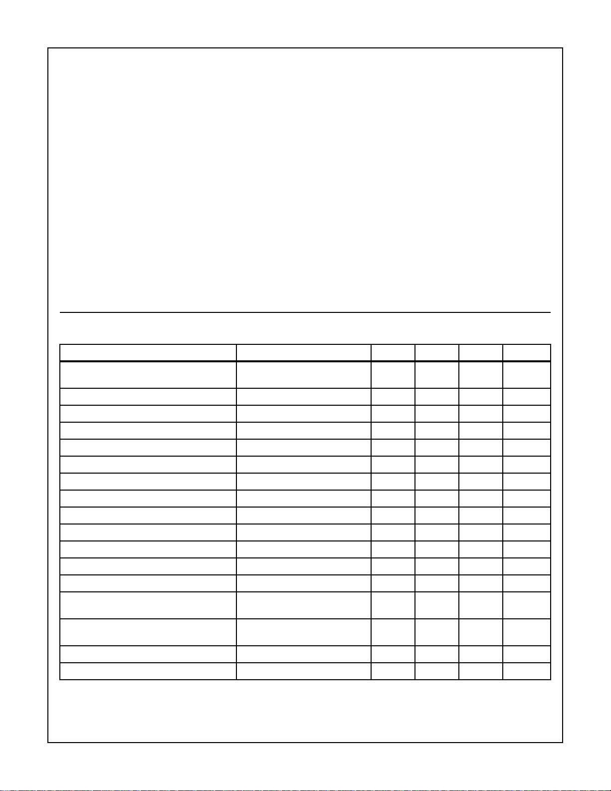
Electrical Specifications Test Conditions: V
= +5V ±10%, TA = Operating Temperature Range. Test Circuit as in Figure 8
CC
Unless Otherwise Specified
PARAMETER TEST CONDITIONS MIN TYP MAX UNITS
Transmitter Output Voltage Swing, T
OUT
T1
OUT
and T2
Loaded with 3kΩ
OUT
±5 ±9 ±10 V
to Ground
Power Supply Current, I
TIN, Input Logic Low, V
TIN, Input Logic High, V
Logic Pullup Current, I
CC
lL
lH
P
RS-232 Input Voltage Range, V
Receiver Input Impedance, R
IN
IN
Outputs Unloaded, TA = 25oC-510mA
- - 0.8 V
2.0 - - V
T1IN, T2IN = 0V - 15 200 µA
-30 - +30 V
VIN = ±3V 3.0 5.0 7.0 kΩ
Receiver Input Low Threshold, VlN (H-L) VCC = 5V, TA = 25oC 0.8 1.2 - V
Receiver Input High Threshold, VIN (L-H) VCC = 5V, TA = 25oC - 1.7 2.4 V
Receiver Input Hysteresis, V
TTL/CMOS Receiver Output Voltage Low, VOLI
TTL/CMOS Receiver Output Voltage High, VOHI
Propagation Delay, t
PD
HYST
= 3.2mA - 0.1 0.4 V
OUT
= -1.0mA 3.5 4.6 - V
OUT
RS-232 to TTL - 0.5 - µs
Instantaneous Slew Rate, SR CL = 10pF, RL = 3kΩ, TA = 25oC
0.2 0.5 1.0 V
- - 30 V/µs
(Notes 2, 3)
Transition Region Slew Rate, SR
T
RL = 3kΩ, CL = 2500pF Measured
-3-V/µs
from +3V to -3V or -3V to +3V
Output Resistance, R
OUT
RS-232 Output Short Circuit Current, I
SC
VCC = V+ = V- = 0V, V
T1
OUT
or T2
Shorted to GND - ±10 - mA
OUT
= ±2V 300 - - Ω
OUT
NOTES:
2. Guaranteed by design.
3. See Figure 4 for definition.
8-50
 Loading...