Intersil Corporation HS-RTX2010RH Datasheet
HS-RTX2010RH
Data Sheet March 2000
Radiation Hardened Real Time Express™
Microcontroller
The HS-RTX2010RH is a radiation-hardened 16-bit
microcontroller with on-chip timers, an interrupt controller, a
multiply-accumulator, and a barrel shifter. It is particularly
well suited for space craft environments where very high
speed control tasks which require arithmetically intensive
calculations, including floating point math to be performed in
hostile space radiation environments.
This processor incorporates two 256-word stacks with
multitasking capabilities, including configurable stack
partitioning and over/underflow control.
Instruction executiontimesof one or two machine cycles are
achieved by utilizing a stack oriented, multiple bus
architecture. The high performance ASIC Bus, which is
unique to the RTX product, provides for extension of the
microcontroller architecture using off-chip hardware and
application specific I/O devices.
RTX Microcontrollers support the C and Forth programming
languages. The advantages of this product are further
enhanced through third party hardware and software support.
Combined, these features make the HS-RTX2010RH an
extremely powerful processor serving numerous
applications in high performance space systems. The
HS-RTX2010RH has been designed for harsh space
radiation environments and features outstanding Single
Event Upset (SEU) resistance and excellent total dose
response.
Specifications for Rad Hard QML devices are controlled
by the Defense Supply Center in Columbus (DSCC). The
SMD numbers listed here must be used when ordering.
Detailed Electrical Specifications for these devices are
contained in SMD 5962-95635. A “hot-link” is provided
on our homepage for downloading.
www.intersil.com/spacedefense/space.asp
Ordering Information
INTERNAL
ORDERING NUMBER
5962F9563501QXC HS8-RTX2010RH-8 55 to 125
5962F9563501QYC HS9-RTX2010RH-8 55 to 125
5962F9563501V9A HS0-RTX2010RH-Q 25
5962F9563501VXC HS8-RTX2010RH-Q 55 to 125
5962F9563501VYC HS9-RTX2010RH-Q 55 to 125
HS8-RTX2010RH/Proto HS8-RTX2010RH/Proto 55 to 125
HS9-RTX2010RH/Proto HS9-RTX2010RH/Proto 55 to 125
MKT. NUMBER
TEMP. RANGE
(oC)
File Number 3961.3
Features
• Electrically Screened to SMD # 5962-95635
• QML Qualified per MIL-PRF-38535 Requirements
• Fast 125ns Machine Cycle
• 1.2µM TSOS4 CMOS/SOS Process
• Total Dose Capability . . . . . . . . . . . . . . . . . . 300KRad(Si)
• Single Event Upset Critical LET . . . . . . . >120MeV/mg/cm
• Single Event Upset Error Rate . . . .<1 x 10
o
C - 125oC, 5V ±10% Operation
• -55
• Single Cycle Instruction Execution
• Fast Arithmetic Operations
- Single Cycle 16-Bit Multiply
- Single Cycle 16-Bit Multiply Accumulate
- Single Cycle 32-Bit Barrel Shift
- Hardware Floating Point Support
• C Software Development Environment
• Direct Execution of Fourth Language
• Single Cycle Subroutine Call/Return
• Four Cycle Interrupt Latency
• On-Chip Interrupt Controller
• Three On-Chip 16-Bit Timer/Counters
• Two On-Chip 256 Word Stacks
• ASIC Bus™ for Off-Chip Architecture Extension
• 1 Megabyte Total Address Space
• Word and Byte Memory Access
• Fully Static Design - DC to 8MHz Operation
• 84 Lead Quad Flat Package or 85 Pin Grid Array
• Third Party Software and Hardware Dev elopment Systems
NOTE: Single Event Upset error rates are Adams 10% worst case
environment under worst case conditions for upset.
-10
Errors/Bit-Day
(Note)
Applications
• Space Systems Embedded Control
• Digital Filtering
• Image Processing
• Scientific Instrumentation
• Optical Systems
• Control Systems
• Attitude/Orbital Control
2
1
CAUTION: These devices are sensitive to electrostatic discharge; follow proper IC Handling Procedures.
1-888-INTERSIL or 321-724-7143
Real Time Express™, RTX™, and ASIC Bus™ are trademarks of Intersil Corporation.
| Copyright © Intersil Corporation 2000
Block Diagram
HS-RTX2010RH
CONTROL
INPUTS
INTERRUPT
INPUTS
TIMER
INPUTS
CLOCK AND
CONFIGURATION
CONTROL
INTERRUPT
CONTROL
TIMER/
COUNTERS
BARREL
SHIFTER
OFF CHIP
PERIPHERALS
ASIC BUS
INTERFACE
RTX CORE
PROCESSOR
MAC
MAIN
MEMORY
MEMORY BUS
INTERFACE
MEMORY
PAGE
CONTROL
HS-RTX2010RH
256-WORD
RETURN
STACK
STACK
CONTROLLERS
256-WORD
PARAMETER
STACK
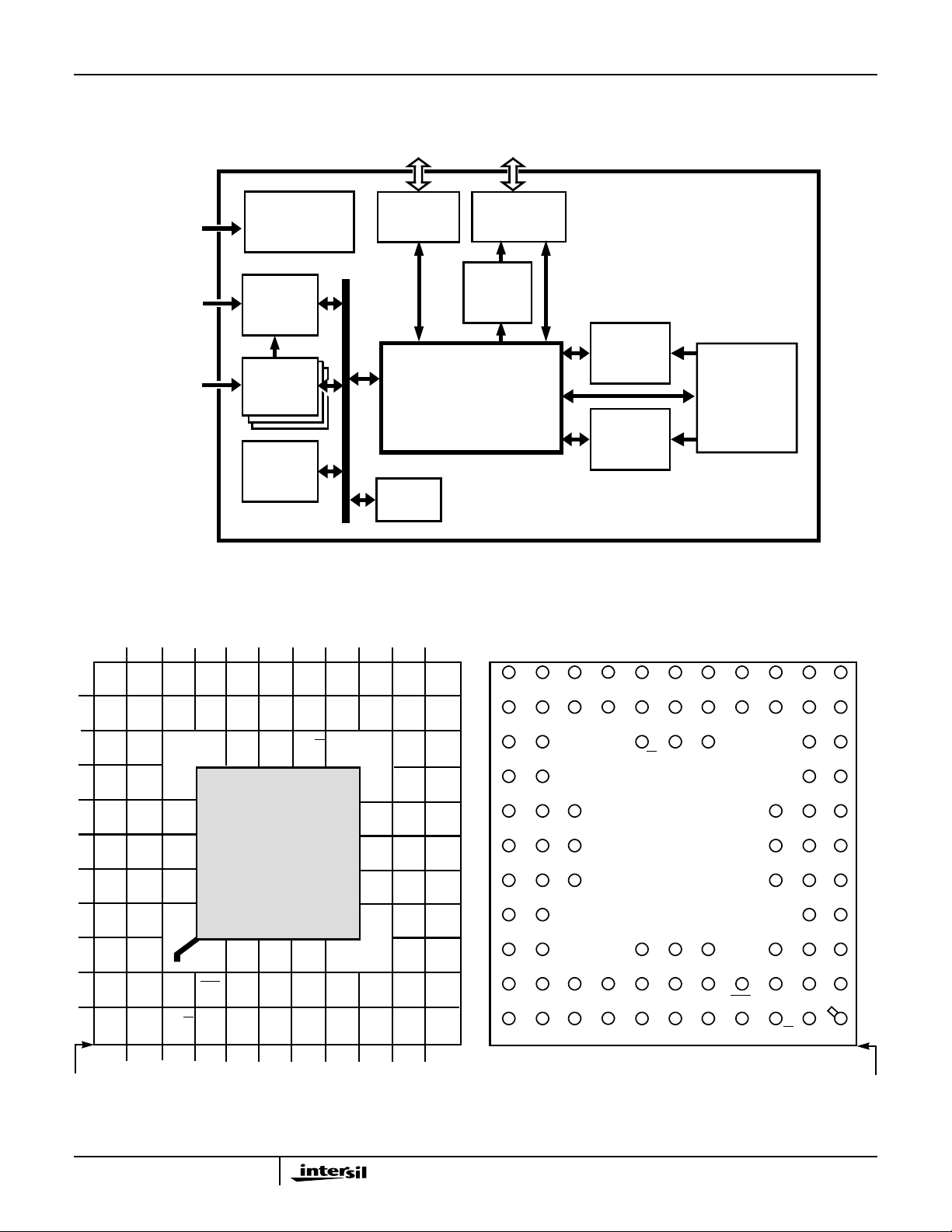
Pinouts
HS8-RTX2010RH
MIL-STD-1835 CMGA3-P85C
BACDEFGHJKL
11
MD08
MD07
MD11
10
PIN
A1
MD09
MD12
MD10
9
MD14
MD13
8
GA00
MD15
7
GND
TCLK
6
INTA
5
4
3
2 RESET
1
NMI
VDD MA02 MA03E I1
E I2 GD14 GD11 GD10E I4
E I3 WAIT GD13 GD12 GD06 GD03 GD02 GD00GD08
E I5 GD15
ICLK
ABCDEFGHJKL
NOTE: An overbar on a signal name represents an active LOW signal.
MD06
VDD
GA01
GA02
INT-
SUP
GR/W
GND
MD05
GIO
MD02
MD01
MD03
NEW
MD04
MD00
HS-RTX2010RH
TOP VIEW
PINS DOWN
GND
GD07
PCLK
BOOT
MR/
UDS
LDS
W
VDD
GND
MA18
GND
MA08
MA04
GD05
MA19
MA16
MA17
MA14
VDD
MA15
MA13
MA12
MA10
MA09
MA07
MA11
MA05
MA06
GD01 MA01
GD04
GNDGD09
MA16
MA14
VDD
MA12
MA09
MA11
MA06
MA03
MA01
GD00
GND
MA19
MA17
MA15
MA13
MA10
MA07
MA05
MA02
GD01
GD02
GD04
GND
MA18
GND
MA08
MA04
GD03
GD05
UDS PCLK
LDS
BOOT
MR/
BOTTOM VIEW
GD10
GD06
GD08
VDD
GD09
MD01
NEW
W
MD00
PINS UP
GD11
GD12
GD07
MD02
MD03
MD04
GD14
GD13
GND
CJKLHGFEDBA
MD10
MD13
W
MD07
MD09
MD15
GND
E I1
E I4
ICLK
MD08
MD11
MD12
MD14
GA00
TCLK
INTA
VDD
E I2
E I5
GND
MD06
MD05
VDD
GA01
GA02
INTSUP NMI
ALIGN.
PIN
GIO
WAIT RESET E I3
GR/
GD15
CJKLHGFEDBA
PIN
A1
11
10
9
8
7
6
5
4
3
2
1
2
Pinouts (Continued)
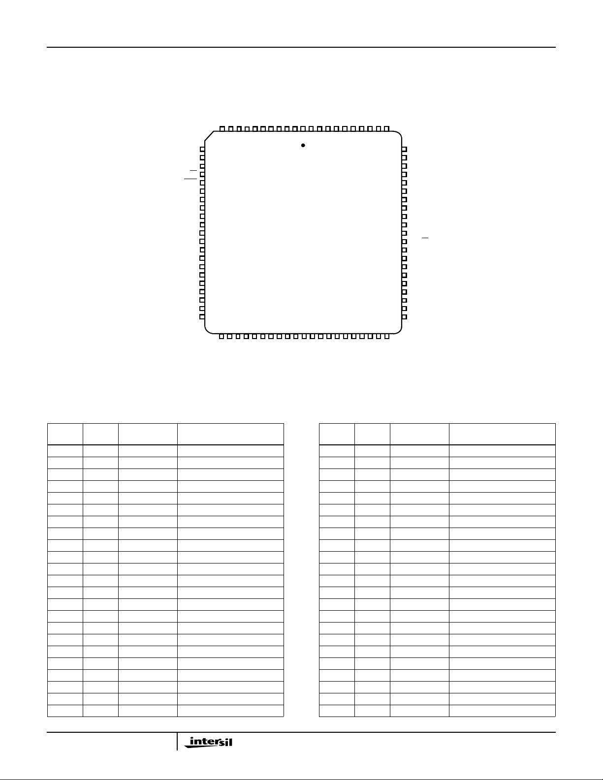
HS-RTX2010RH
HS9-RTX2010RH
(LEAD LENGTH NOT TO SCALE) SEE INTERSIL OUTLINE R84.A
RESET
WAIT
ICLK
GR/W
GIO
GD15
GD14
GD13
GND
GD12
GD11
GD10
GD09
GD08
GD07
VDD
GD06
GD05
GD04
GD03
GND
EI5
EI2
EI3
EI4
8
9
10
11
12
13
14
15
16
17
18
19
20
21
22
23
24
25
26
27
28
29
30
31
32
36
35
34
GD00
GD01
GD02
MA01
VDD
EI1
38
37
MA03
MA02
INTSUP
567
39
MA04
NMI
4
HS-RTX2010RH
40
MA05
NOTE: An overbar on a signal name represents an active LOW signal.
PGA And CQFP
Pin/Signal Assignments
PGA
CQFP
PIN
1 C6 GA02 Output; Address Bus
2 A6 TCLK Output
3 A5 INTA Output
4 B5 NMI Input
5 C5 INTSUP Input
6 A4 VDD Power
7 B4 EI1 Input
8 A3 EI2 Input
9 A2 EI3 Input
10 B3 EI4 Input
11 A1 EI5 Input
12 B2 RESET Input
13 C2 WAIT Input
14 B1 ICLK Input
15 C1 GR/W Output
16 D2 GIO Output
17 D1 GD15 I/O; Data Bus
18 E3 GD14 I/O; Data Bus
19 E2 GD13 I/O; Data Bus
20 E1 GND Ground
21 F2 GD12 I/O; Data Bus
22 F3 GD11 I/O; Data Bus
23 G3 GD10 I/O; Data Bus
SIGNAL
NAME TYPE
GA02
TCLK
INTA
1
2
3
TOP VIEW
43
42
41
MA08
MA07
MA06
MD09
MD10
MD11
MD12
MD13
MD14
GND
MD15
GA00
GA01
75
76
77
78
79
80
81
82
83
84
44
GND
46
45
MA10
MA09
48
47
MA12
MA11
MA13
503349
VDD
52
51
MA15
MA14
74
73
72
71
70
69
68
67
66
65
64
63
62
61
60
59
58
57
56
55
54
53
MA16
MD08
VDD
MD07
MD06
MD05
GND
MD04
MD03
MD02
MD01
MD00
MR/
PCLK
BOOT
NEW
UDS
LDS
GND
MA19
MA18
MA17
W
PGA And CQFP
Pin/Signal Assignments
PGA
CQFP
PIN
24 G1 GD09 I/O; Data Bus
25 G2 GD08 I/O; Data Bus
26 F1 GD07 I/O; Data Bus
27 H1 VDD Power
28 H2 GD06 I/O; Data Bus
29 J1 GD05 I/O; Data Bus
30 K1 GD04 I/O; Data Bus
31 J2 GD03 I/O; Data Bus
32 L1 GND Ground
33 K2 GD02 I/O; Data Bus
34 K3 GD01 I/O; Data Bus
35 L2 GD00 I/O; Data Bus
36 L3 MA01 Output; Address Bus
37 K4 MA02 Output; Address Bus
38 L4 MA03 Output; Address Bus
39 J5 MA04 Output; Address Bus
40 K5 MA05 Output; Address Bus
41 L5 MA06 Output; Address Bus
42 K6 MA07 Output; Address Bus
43 J6 MA08 Output; Address Bus
44 J7 GND Ground
45 L7 MA09 Output; Address Bus
46 K7 MA10 Output; Address Bus
SIGNAL
NAME TYPE
(Continued)
3

HS-RTX2010RH
PGA And CQFP
Pin/Signal Assignments
PGA
CQFP
47 L6 MA11 Output; Address Bus
48 L8 MA12 Output; Address Bus
49 K8 MA13 Output; Address Bus
50 L9 VDD Power
51 L10 MA14 Output; Address Bus
52 K9 MA15 Output; Address Bus
53 L11 MA16 Output; Address Bus
54 K10 MA17 Output; Address Bus
55 J10 MA18 Output; Address Bus
56 K11 MA19 Output; Address Bus
57 J11 GND Ground
58 H10 LDS Output
59 H11 UDS Output
60 F10 NEW Output
61 G10 BOOT Output
62 G11 PCLK Output
63 G9 MR/W Output
64 F9 MD00 I/O; Data Bus
65 F11 MD01 I/O; Data Bus
PIN
SIGNAL
NAME TYPE
(Continued)
PGA And CQFP
Pin/Signal Assignments
PGA
CQFP
66 E11 MD02 I/O; Data Bus
67 E10 MD03 I/O; Data Bus
68 E9 MD04 I/O; Data Bus
69 D11 GND Ground
70 D10 MD05 I/O; Data Bus
71 C11 MD06 I/O; Data Bus
72 B11 MD07 I/O; Data Bus
73 C10 VDD Power
74 A11 MD08 I/O; Data Bus
75 B10 MD09 I/O; Data Bus
76 B9 MD10 I/O; Data Bus
77 A10 MD11 I/O; Data Bus
78 A9 MD12 I/O; Data Bus
79 B8 MD13 I/O; Data Bus
80 A8 MD14 I/O; Data Bus
81 B6 GND Ground
82 B7 MD15 I/O; Data Bus
83 A7 GA00 Output; Address Bus
84 C7 GA01 Output; Address Bus
- C3 - Isolated Alignment Pin
PIN
SIGNAL
NAME TYPE
(Continued)
Output Signal Descriptions
RESET
SIGNAL CQFP
OUTPUTS
NEW 60 1 NEW: A HIGH on this pin indicates that an Instruction Fetch is in progress.
BOOT 61 1 BOOT: A HIGH on this pin indicates that Boot Memory is being accessed. This pin can be set or reset by accessing
MR/W 63 1 MEMORY READ/WRITE: A LOW on this pin indicates that a Memory Write operation is in progress.
UDS 59 1 UPPER DATA SELECT: A HIGH on this pin indicates that the high byte of memory (MD15-MD08) is being
LDS 58 1 LOWER DATA SELECT: A HIGH on this pin indicates that the low byte of memory (MD07-MD00) is being
GIO 16 1 ASIC I/O: A LOW on this pin indicates that an ASIC Bus operation is in progress.
GR/W 15 1 ASIC READ/WRITE: A LOW on this pin indicates that an ASIC Bus Write operation is in progress.
PCLK 62 0 PROCESSOR CLOCK: Runs at half the frequency of ICLK. All processor cycles begin on the rising edge of PCLK.
TCLK 2 0 TIMING CLOCK: Same frequency and phase as PCLK but continues running during Wait cycles.
INTA 3 0 INTERRUPT ACKNOWLEDGE: A HIGH on this pin indicates that an Interrupt Acknowledge cycle is in progress.
LEVEL DESCRIPTION
bit 3 of the Configuration Register.
accessed.
accessed.
Held low extra cycles when WAIT is asserted.
Input Signal, Bus, and Power Connection Descriptions
CQFP
SIGNAL
INPUTS
WAIT 13 WAIT: A HIGH on this pin causes PCLK to be held LOW and the current cycle to be extended.
ICLK 14 INPUT CLOCK: Internally divided by 2 to generate all on-chip timing (CMOS input levels).
RESET 12 A HIGH level on this pin resets the RTX. Must be held high for at least 4 rising edges of ICLK plus 12 ICLK cycle
LEAD DESCRIPTION
setup and hold times.
4
HS-RTX2010RH
Input Signal, Bus, and Power Connection Descriptions (Continued)
CQFP
SIGNAL
EI2, EI1 8, 7 EXTERNALINTERRUPTS 2, 1: Active HIGH level-sensitive inputs to the Interrupt Controller. Sampled on the rising
EI5-EI3 11-9 EXTERNAL INTERRUPTS 5, 4, 3: Dual purpose inputs; active HIGH level-sensitive Interrupt Controller inputs;
NMI 4 NON-MASKABLE INTERRUPT: Active HIGH edge-sensitive Interrupt Controller input capable of interrupting any
INTSUP 5 INTERRUPT SUPPRESS: A HIGH on this pin inhibits all maskable interrupts, internal and external.
ADDRESS BUSES (OUTPUTS)
GA02 1 ASIC ADDRESS: 3-bit ASIC Address Bus, which carries address information for external ASIC devices.
GA01 84
GA00 83
MA19-MA14 56-51 MEMORY ADDRESS: 19-bit Memory Address Bus, which carries address information for Main Memory.
MA13-MA09 49-45
MA08-MA01 43-36
DATA BUSES (I/O)
GD15-GD13 17-19 ASIC DATA: 16-bit bidirectional external ASIC Data Bus, which carries data to and from off-chip I/O devices.
GD12-GD07 21-26
GD06-GD03 28-31
GD02-GD00 33-35
MD15 82 MEMORY DATA: 16-bit bidirectional Memory Data Bus, which carries data to and from Main Memory.
MD14-MD08 80-74
MD07-MD05 72-70
MD04-MD00 68-64
POWER CONNECTIONS
VDD 6, 27,
GND 20, 32,
LEAD DESCRIPTION
edge of PCLK. See Timing Diagrams for detail.
active HIGH edge-sensitive Timer/Counter inputs. As interrupt inputs, they are sampled on the rising edge of PCLK.
See Timing Diagrams for detail.
processor cycle when NMI is set to Mode 0. See the Interrupt Suppression and Interrupt Controller Sections.
Power supply +5V connections. A 0.1µF, low impedance decoupling capacitor should be placed between VDD and
50, 73
GND. This should be located as close to the RTX package as possible.
Power supply ground return connections.
44, 57,
69, 81
TYPICAL
CLOCK OR
STROBE
TYPICAL
INPUT
TYPICAL
OUTPUT
TYPICAL
DAT A
OUTPUT
4.0V
0.5V
4.0V
0.5V
t
PULSE WIDTH
2.25V
t
DELAY
t
VALID
t
SETUP
2.25V
2.25V
2.75V
1.75V
t
PULSE WIDTH
2.25V
t
HOLD
2.25V
t
DELAY
t
HOLD
2.75V
1.75V
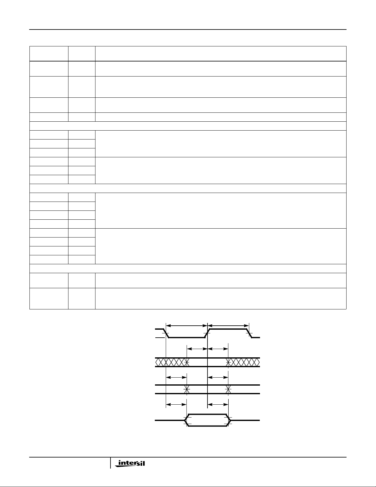
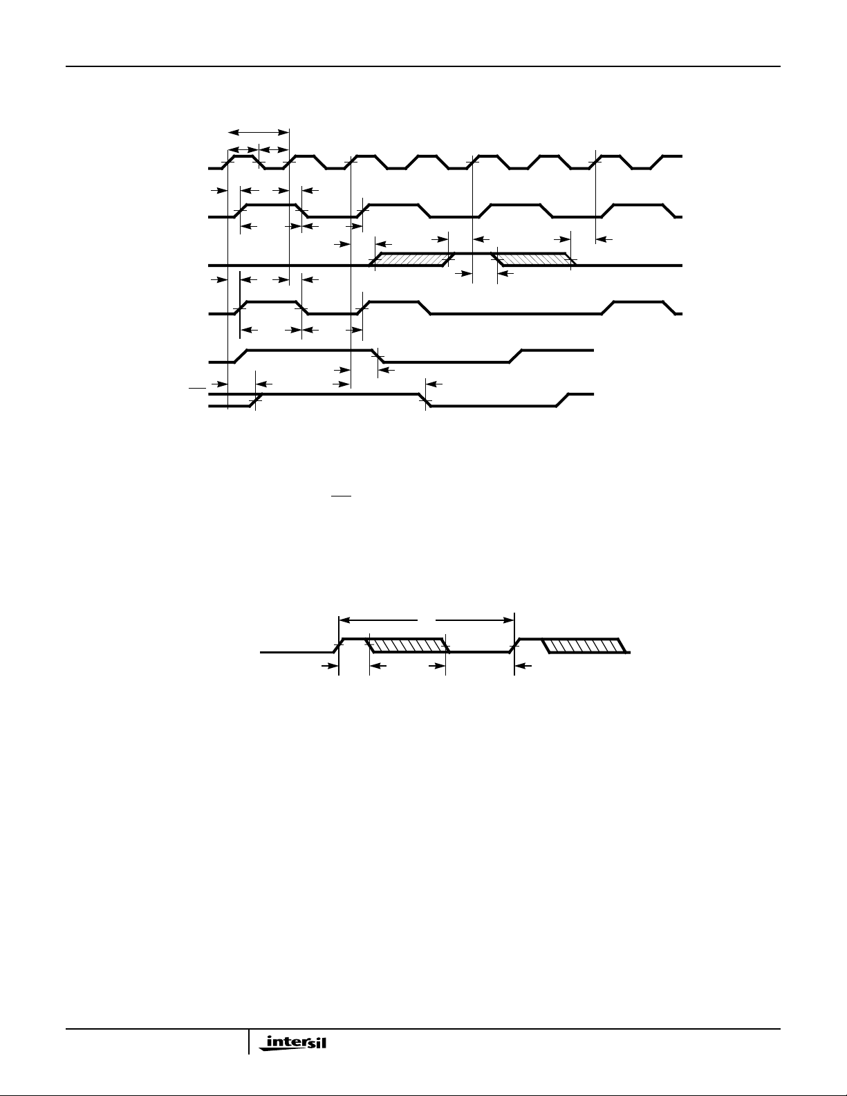
FIGURE 1. AC DRIVE AND MEASURE POINTS - CLK INPUT
5
2.25V
2.25V
Timing Diagrams
ICLK
HS-RTX2010RH
t
1
t
t
3
2
t
TCLK
WAIT
PCLK
(NOTE 1)
PCLK
(NOTE 2)
GIO
(NOTE 3)
11
t
13
t
15
t
17
t
51
t
19
t
12
t
5
t
20
t
16
t
20
t
4
t
5
t
50
t
4
NOTES:
1. NORMAL CYCLE: This waveform describes a normal PCLK cycle and a PCLK cycle with a Wait state.
2. EXTENDED CYCLE: This waveform describes a PCLK cycle for a USER memory access or an external ASIC Bus read cycle when the CYCEXT
bit or ARCE bit is set.
3. EXTENDED CYCLE: This waveform describes a GIO cycle for an external ASIC Bus read when the ARCE bit is set.
4. An active HIGH signal on the RESET input is guaranteed to reset the processor if its duration is greater than or equal to 4 rising edges of ICLK
plus 1/2 ICLK cycle setup and hold times. If the RESET input is active for less than four rising edges of ICLK, the processor will not reset.
FIGURE 2. CLOCK AND WAIT TIMING
EI5 - EI3
t
6
t
7
t
8
FIGURE 3. TIMER/COUNTER TIMING
6
Timing Diagrams (Continued)
PCLK
HS-RTX2010RH
MA
LDS
UDS
NEW
BOOT
MR/
MD
MD
OUT
t
26
t
29
t
W
IN
t
t
34
32
21
t
28
t
31
t
22
t
35
t
33
NOTES:
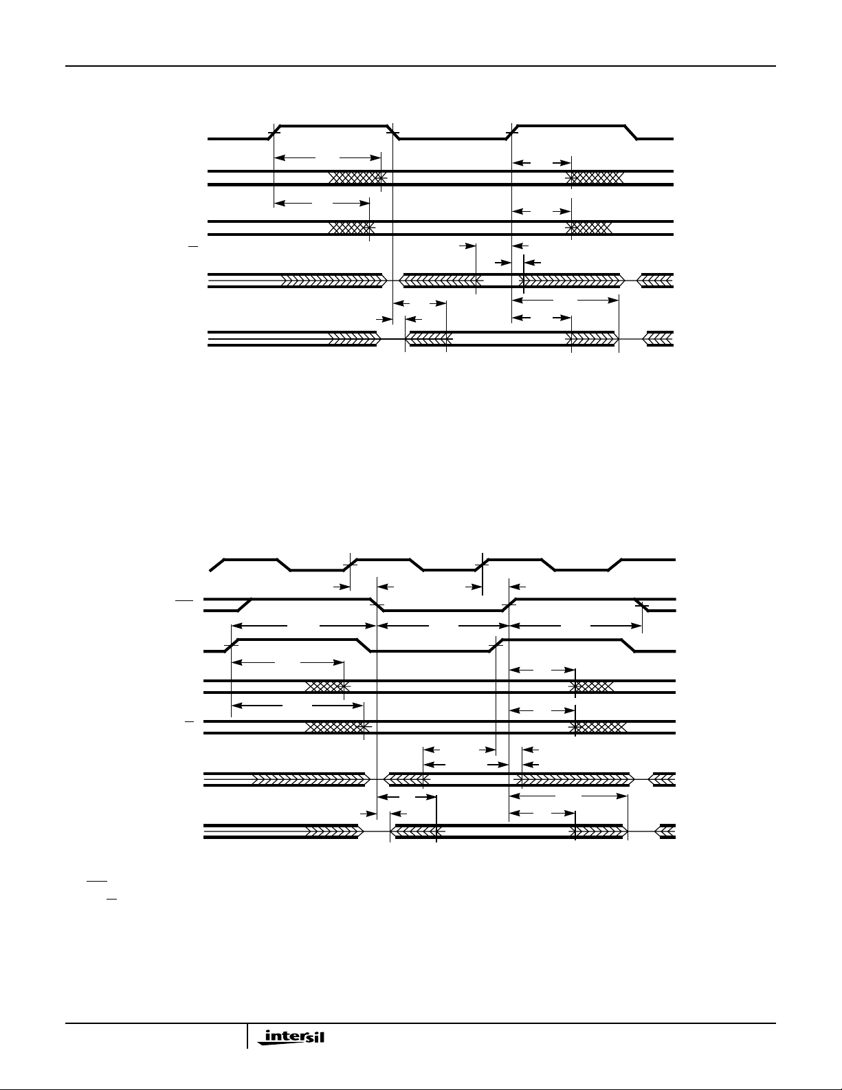
5. If both LDS and UDS are low, no memory access is taking place in the current cycle. This only occurs during streamed instructions that do not
access memory.
6. During a streamed single cycle instruction, the Memory Data Bus is driven by the processor.
FIGURE 4. MEMORY BUS TIMING
ICLK
GIO
PCLK
GR/
OUT
GA
GD
GD
t
50
t
48
t
52
t
56
W
IN
t
61
t
49
t
40A, B
t
41A, B
t
62
t
51
t
69
t
54
t
58
t
43
t
42
t
65
t
63
NOTES:
7. GIO remains high for internal ASIC bus cycles.
8. GR/W goes low and GD is driven for all ASIC write cycles, including internal ones.
9. During non-ASIC write cycles, GD is not driven by the HS-RTX2010RH. Therefore, it is recommended that all GD pins be pulled to VCC or GND
to minimize power supply current and noise.
10. t
40B
and t
specifications are for Streamed Mode of operation only.
41B
FIGURE 5. ASIC BUS TIMING
7
Timing Diagrams (Continued)
HS-RTX2010RH
PCLK
INTSUP
INTA
MA
e
EI
e
1
2
t
44
e
3
t
46t47
e
4
t
46t47
e
5
t
67
t
26
INT VECTOR
t
68
t
28
NOTES:
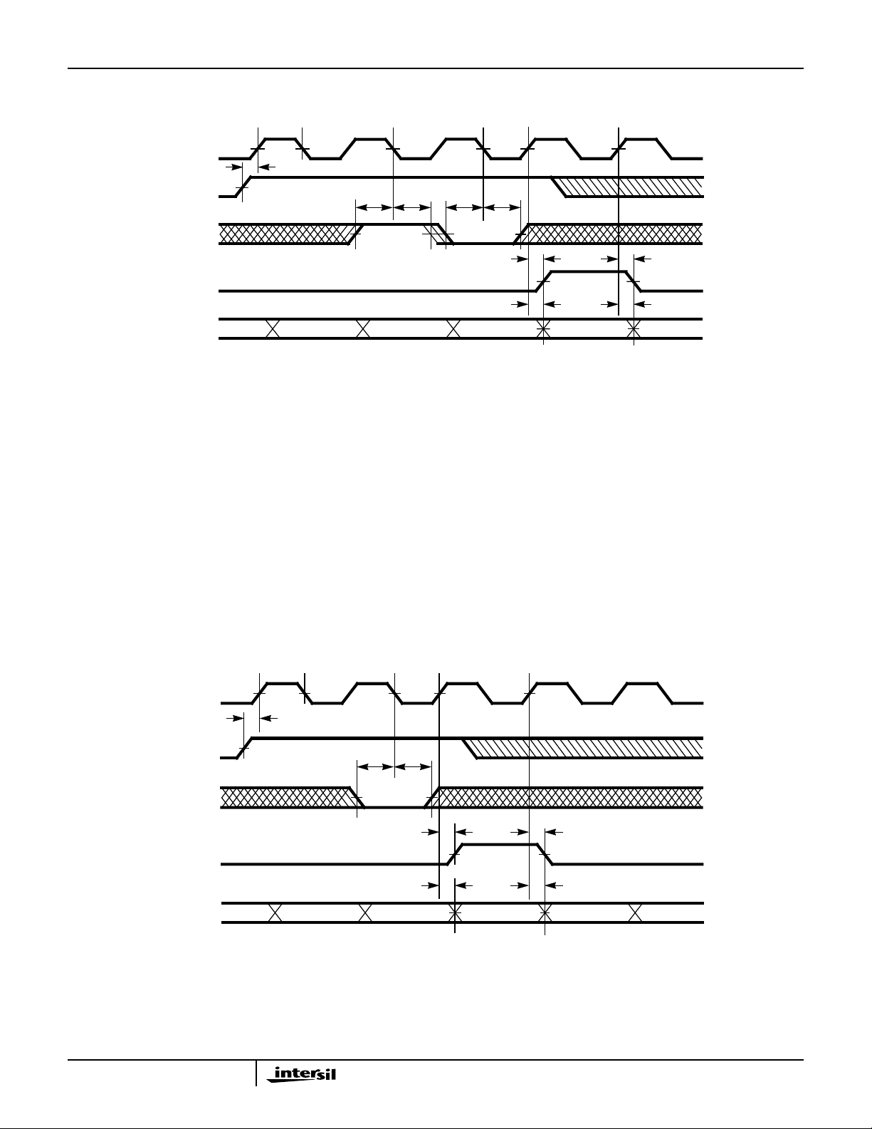
11. Events in an interrupt sequence are as follows:
e1. The Interrupt Controller samples the interrupt request inputs on the rising edge of PCLK. If NMI rises between e1and the rising edge of
PCLK prior to e5, the interrupt vector will be for NMI.
e2. If any interrupt requests were sampled, the Interrupt Controller issues an interrupt request to the core on the falling edge of PCLK.
e3. The core samples the state of the interrupt requests from the Interrupt Controller on the falling edge of PCLK. If INTSUP is high, maskable
interrupts will not be detected at this time.
e4. When the core samples an interrupt request on the falling edge of PCLK, an Interrupt Acknowledge cycle will begin on the next rising edge
of PCLK.
e5. Following the detection of an interrupt request by the core, an Interrupt Acknowledge cycle begins. The interrupt vector will be based on the
highest priority interrupt request active at this time.
12. t44 is only required to determine when the Interrupt Acknowledge cycle will occur.
13. Interrupt requests should be held active until the Interrupt Acknowledge cycle for that interrupt occurs.
FIGURE 6. INTERRUPT TIMING: WITH INTERRUPT SUPPRESSION
PCLK
INTSUP
INTA
MA
EI
e
e
1
2
t
44
e
4
t
46t47
e
5
t
67
t
26
INT VECTOR
t
68
t
28
FIGURE 7. INTERRUPT TIMING: WITH NO INTERRUPT SUPPRESSION
8
Timing Diagrams (Continued)
HS-RTX2010RH
e
1
PCLK
t
44
NMI
INTA
MA
NOTES:
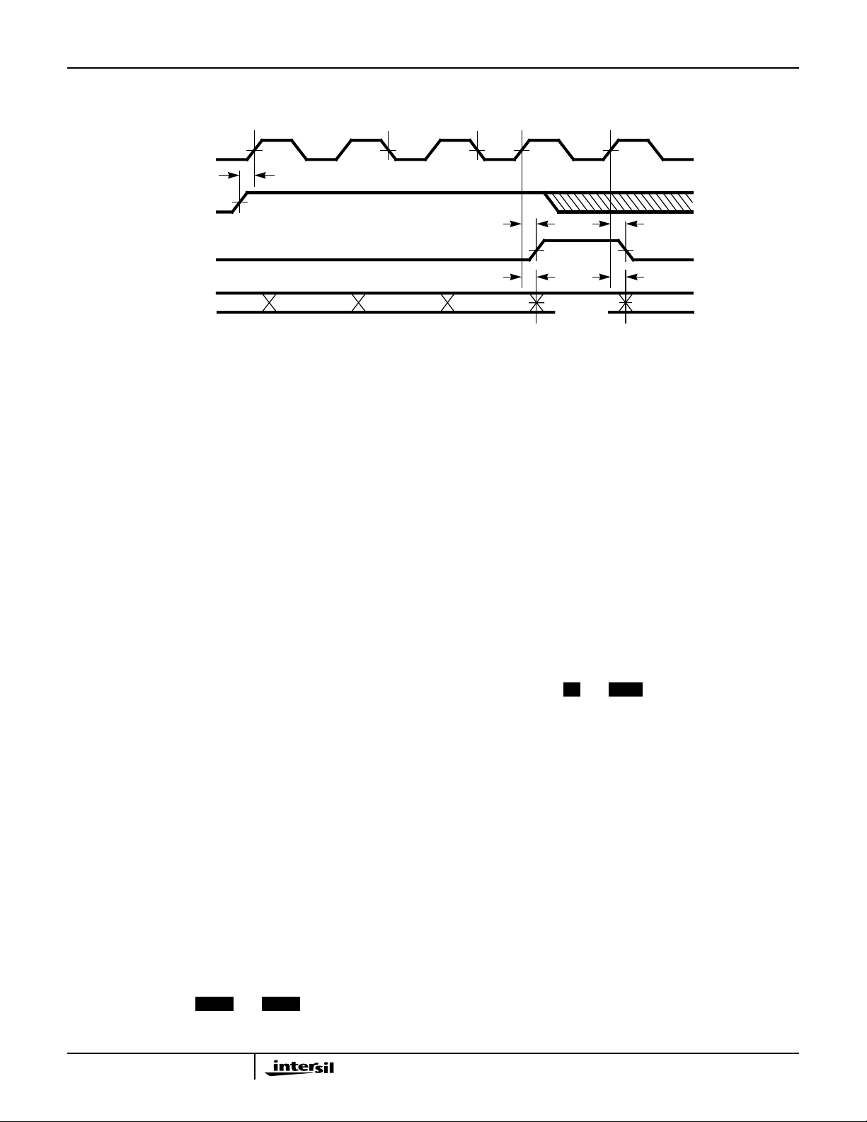
14. Events in an interrupt sequence are as follows:
e1. The Interrupt Controller samples the interrupt request inputs on the rising edge of PCLK. If NMI rises between e1and the rising edge of
PCLK prior to e5, the interrupt vector will be for NMI.
e2. If any interrupt requests were sampled, the Interrupt Controller issues an interrupt request to the core on the falling edge of PCLK.
e4. When the core samples an interrupt request on the falling edge of PCLK, an Interrupt Acknowledge cycle will begin on the next rising edge
of PCLK.
e5. Following the detection of an interrupt request by the core, an Interrupt Acknowledge cycle begins. The interrupt vector will be based on the
highest priority interrupt request active at this time.
15. t44 is only required to determine when the Interrupt Acknowledge cycle will occur.
16. Interrupt requests should be held active until the Interrupt Acknowledge cycle for that interrupt occurs.
17. NMI has a glitch filter which requires the signal that initiates NMI last at least two rising and two falling edges of ICLK.
FIGURE 8. NON-MASKABLE INTERRUPT TIMING
e
2
e
e
4
5
t
67
t
26
NMI
VECTOR
t
68
t
28
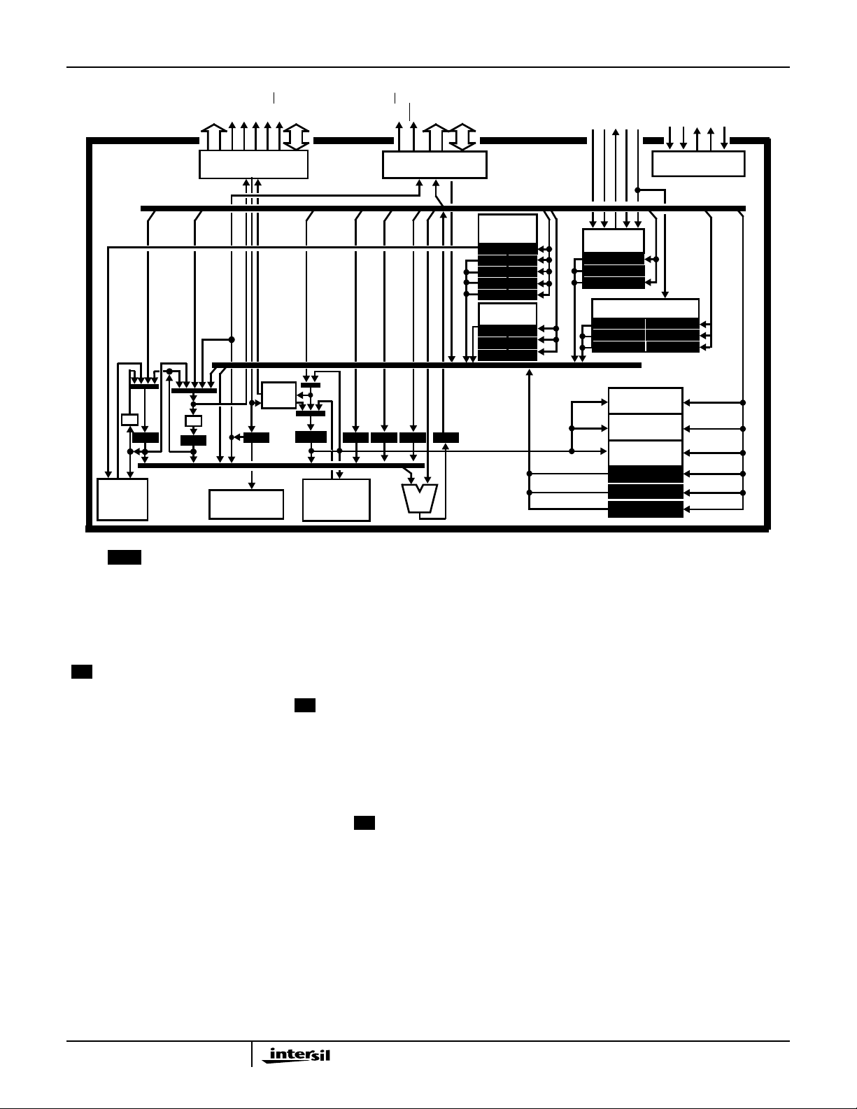
HS-RTX2010RH Microcontroller
The HS-RTX2010RH is designed around the RTX Processor
core, which is part of the Intersil Standard Cell Library.
This processor core has eight 16-bit internal registers, an
ALU, internal data buses, and control hardware to perform
instruction decoding and sequencing.
On-chip peripherals which the HS-RTX2010RH includes are
Memory Page Controller, an Interrupt Controller, three
Timer/Counters, and two Stack Controllers. Also included
are a Multiplier-Accumulator (MAC), a Barrel Shifter, and a
Leading Zero Detector for floating point support.
Off-chip user interfaces provide address and data access to
Main Memory and ASIC I/O devices, user defined interrupt
signals, and Clock/Reset controls.
Figure 9 shows the data paths between the core, on-chip
peripherals, and off-chip interfaces.
The HS-RTX2010RH microcontroller is based on a two-stack
architecture. These two stacks, which are Last-In-First-Out
(LIFO) memories, are called the Parameter Stack and the
Return Stack.
Two internal registers, and , provide the top
two elements of the 16-bit wide Parameter Stack, while the
TOP NEXT
remaining elements are contained in on-chip memory (“stack
memory”).
The top element of the Return Stack is 21 bits wide, and is
stored in registers and , while the remaining
I IPR
elements are contained in stack memory.
The highly parallel architecture of the RTX is optimized for
minimal Subroutine Call/Return overhead. As a result, a
Subroutine Call takes one Cycle, while a Subroutine Return
is usually incorporated into the preceding instruction and
does not add any processor cycles. This parallelism
provides for peak execution rates during simultaneous bus
operations which can reach the equivalent of 32 million
Forth language operations per second at a clock rate of
8MHz. Typical execution rates exceed 8 million operations
per second.
Intersil factory applications support for this device is limited.
RTS-C C-Compiler support is provided by Highland Software
at highlandsoft@compuserve.com. Development system
tools are supported by Micro Processor Engineering Limited
(UK) at 441 703 631441. A HS-RTX2010RH programmers
reference manual can be obtained through your local Intersil
Sales Office.
9
OFF-CHIP
USER
INTERFACES
MA01
MA19-
UDS
LDS
NEW
BOOT
MR/W
MD15-
MD00
HS-RTX2010RH
GIO
GA2-
GR/W
GA0
GD15-
GD00
INTA
NMI
INTSUP
EI5-EI3
EI2-EI1
ICLK
WAIT
PCLK
TCLK
RESET
+1
PC
INSTRUCTION
MEMORY BUS
INTERFACE
BYTE
SWAP
IR
DECODER
NEXT
256 x 16
PARAMETER
STACK
MEMORY
HS-RTX2010RH
-1
I
256 x 21
RETURN
STACK
MEMORY
NOTE: contains the 5 most significant bits (20-16) of the top element of the Return Stack.
IPR
ASIC BUS
INTERFACE
TOPCR MD SR
YT
ALU
MEMORY
PAGE
CONTROL
(NOTE)
STACK
CONTROL
IPR
DPR
UPR
CPR
UBR
SPR
SVR
SUR
FIGURE 9. HS-RTX2010RH FUNCTIONAL BLOCK DIAGRAM
INTERRUPT
CONTROL
IMR
IVR
IBC
TIMER/COUNTERS
TC0
TC1
TC2
BARREL
SHIFTER
LEADING ZERO
DETECTOR
16 x 16
MAC
MXR
MHR
MLR
CLOCK AND
CONTROLRESET
TP0
TP1
TP2
HS-RTX2010RH Operation
Control of all data paths and the Program Counter Register,
( ), is provided by the Instruction Decoder. This hardware
PC
determines what function is to be performed by looking at
the contents of the Instruction Register, ( ), and
subsequently determines the sequence of operations
through data path control.
Instructions which do not perform memory accesses execute
in a single clock cycle while the next instruction is being
fetched.
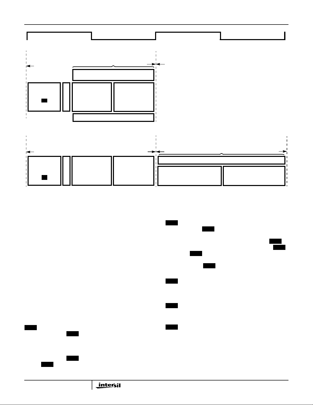
As shown in Figure 10, the instruction is latched into at
the beginning of a clockcycle. The instructionis then decoded
by the processor. All necessary internal operations are
performed simultaneously with fetching the ne xt instruction.
IR
IR
Instructions which access memory require two clock cycles
to be executed. During the first cycle of a memory access
instruction, the instruction is decoded, the address of the
memory location to be accessed is placed on the Memory
Address Bus (MA19-MA01), and the memory data
(MD15-MD00), is read or written. During the second cycle,
ALU operations are performed, the address of the next
instruction to be executedis placed on the Memory Address
Bus, and the next instruction is fetched, as indicated in the
bottom half of Figure 10.
10
PCLK
HS-RTX2010RH
EXECUTION SEQUENCE WITH NO MEMORY DATA ACCESS:
BEGIN
FIRST
CLOCK
CYCLE
PERFORM INTERNAL OPERATIONS AND
ALU OPERATIONS, AS REQUIRED
INSTRUCTION
LATCHES INTO
IR
EXECUTION SEQUENCE WITH MEMORY DATA ACCESS:
BEGIN
FIRST
CLOCK
CYCLE
INSTRUCTION
LATCHES
INTO
IR
ADDRESS OF
INSTRUCTION
IS PLACED ONTO
MA19-MA01
DECODE
ADDRESS OF
MEMORY
LOCATION
IS PLACED ONTO
MA19-MA01
DECODE
CONCURRENT
OPERATIONS
NEXT
BUS
ASIC BUS OPERATIONS
READ OR WRITE
MEMORY DATA
BUS
FETCH
END OF
FIRST
CLOCK
CYCLE
END OF
FIRST
CLOCK
CYCLE
BEGIN
SECOND
CLOCK
CYCLE
BEGIN
SECOND
CLOCK
CYCLE
PLACE ADDRESS OF
NEXT INSTRUCTION
ONTO MA19-MA01
CONCURRENT
OPERATIONS
PERFORM ALU OPERATIONS
FETCH NEXT
INSTRUCTION
END OF
SECOND
CLOCK
CYCLE
FIGURE 10. INSTRUCTION EXECUTION SEQUENCE
RTX Data Buses and Address Buses
The RTX core bus architecture provides for unidirectional
data paths and simultaneous operation of some data buses.
This parallelism allows for maximum efficiency of data flow
internal to the core.
Addresses for accessing external (off-chip) memory or
ASIC devices are output via either the Memory Data Bus
(MA19-MA01) or the ASIC Address Bus (GA02-GA00). See
Table 3. External data is transferred by the ASIC Data Bus
(GD15-GD00) and the Memory Data Bus (MD15-MD00),
both of which are bidirectional.
RTX Internal Registers
The core of the HS-RTX2010RH is a macrocell available
through the Intersil Standard Cell Library. This core contains
eight 16-bit internal registers, which may be accessed
implicitly or explicitly, depending upon the register accessed
and the function being performed.
: The Top Register contains the top element of the
TOP
Parameter Stack++. is the implicit data source or
destination for certain instructions, and has no ASIC address
assignment. The contents of this register may be directed to
any I/O device or to any processor register except the
Instruction Register. is also the T input to the ALU.
Input to must come through the ALU. This register
TOP
TOP
TOP
also holds the most significant 16 bits of 32-bit products and
32-bit dividends.
: The Next Register holds the second element of the
NEXT
Parameter Stack. is the implicit data source or
EXT
destination for certain instructions, and has no ASIC address
assignment. During a stack “push”, the contents of
are transferred to stack memory, and the contents of
are put into . This register is used to hold the least
NEXT
NEXT
TOP
significant 16 bits of 32-bit products. Memory data is
accessed through , as described in the Memory
NEXT
Access section of this document.
: The Instruction Register is actually a latch which
IR
contains the instruction currently being executed, and has no
ASIC address assignment. In certain instructions, an
operand can be embedded in the instruction code, making
the implicit source for that operand (as in the case of
IR
short literals). Input to this register comes from Main
Memory (see Tables 6 thru 22 for code information).
: The Configuration Register is used to indicate and
CR
control the current status/setup of the RTX microcontroller,
through the bit assignments shown in Figure 11. This
register is accessed explicitly through read and write
operations, which cause interrupts to be suppressed for one
cycle, guaranteeing that the next instruction will be
performed before an Interrupt Acknowledge cycle is allowed
to be performed.
11
 Loading...