

Intersil Corporation HSP9520, HSP9521 Datasheet
HSP9520, HSP9521
Data Sheet May 1999
Multilevel Pipeline Registers
These devices are multilevel pipeline registers implemented
using a low power CMOS process. They are pin for pin
compatible replacements for industry standard multilevel
pipeline registers such as the L29C520 and L29C521. The
HSP9520 and HSP5921 are direct replacements for the
AM29520 and AM29521 and WS59520 and WS59521.
They consist of four 8-bit registers which are dual ported.
They can be configured as a single four level pipeline or a
dual two level pipeline. A single 8-bit input is provided, and
the pipelining configuration is determined by the instruction
code input to the I0 and I1 inputs (see instruction control).
The contents of any of the four registers is selectable at the
multiplexed outputs through the use of the S0 and S1
multiplexercontrol inputs (see register select. The output is 8
bits wide and is three-stated through the use ofthe
OE input.
The HSP9520 and HSP9521 differ only in the way data is
loaded into and between the registers in dual two-level
operation. In the HSP9520 when data is loaded into the first
levelthe existingdata inthe firstlevel is movedto thesecond
level. In the HSP9521 loading the first level simply causes
the current data to be overwritten. Transfer of data to the
second level is achievedusing the singlefour level mode(I1,
I0 = ‘0’). This instruction also causes the first level to be
loaded. TheHOLD instruction (I1, I0 = ‘1’) providesa means
of holding the contents of all registers.
Ordering Information
TEMP.
PART NUMBER
HSP9520CP 0 to 70 24 Ld PDIP E24.3
HSP9520CS 0 to 70 24 Ld SOIC M24.3
HSP9521CP 0 to 70 24 Ld PDIP E24.3
HSP9521CS 0 to 70 24 Ld SOIC M24.3
RANGE (oC) PACKAGE
PKG.
NO.
File Number
Features
• Four 8-Bit Registers
• Hold, Transfer and Load Instructions
• Single 4-Stage or Dual-2 Stage Pipelining
• All Register Contents Available at Output
• Fully TTL Compatible
• Three-State Outputs
• High Speed, Low Power CMOS
Applications
• Array Processor
• Digital Signal Processor
• A/D Buffer
• Telecommunication
• Byte Wide Shift Register
• Mainframe Computers
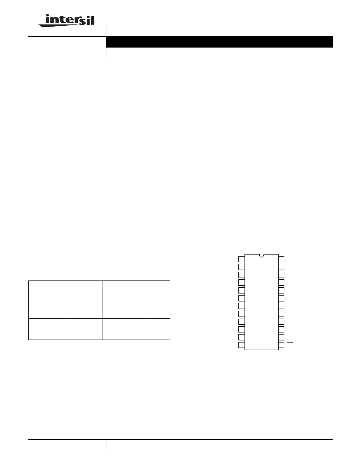
Pinout
HSP9520, HSP9521 (SOIC, PDIP)
TOP VIEW
V
24
23
S0
S1
22
Y0
21
Y1
20
Y2
19
Y3
18
Y4
17
16
Y5
Y6
15
Y7
14
OE
13
D0
D1
D2
D3
D4
D5
D6
D7
CLK
GND
I0
1
I1
2
3
4
5
6
7
8
9
10
11
12
2811.5
CC
1
CAUTION: These devices are sensitive to electrostatic discharge; follow proper IC Handling Procedures.
http://www.intersil.com or 407-727-9207 | Copyright © Intersil Corporation 1999
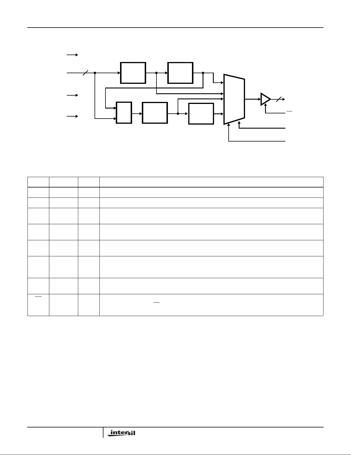
Block Diagram
I0
HSP9520, HSP9521
D0 - D7
CLK
8
I1
REG. A1 REG. A2
MUX
REG. B1
REG. B2
MUX
8
Y0 - Y7
OE
S0
S1
Pin Descriptions
NAME DIP PIN TYPE DESCRIPTION
V
CC
GND 12 The device ground.
CLK 11 I Input Clock. Data is latched on the low to high transition of this clock signal. Input setup and hold times with
D0-7 3-10 I Data Input Port. These inputs are used to supply the 8 bits of data which will be latched into the selected
24 The +5V Power Supply Pin. A 0.1µF capacitor between the VCC and GND pin is recommended.
respect to the clock must be met for proper operation.
register on the next rising clock edge.
Y0-7 21-14 O DataOutput Port. This 8-bit portprovides the output data fromthe four internalregisters. Theyare provided in
a multiplexed fashion, and are controlled via the multiplexer control inputs (S0 and S1).
I0, I1 1, 2 I InstructionControl Inputs. Theseinputs are usedto provide theinstruction code whichdetermines the internal
registerpipeline configuration. Refer totheInstructionControl Table forthespecificcodes and their associated
configurations.
S0, S1 23, 22 I Multiplexer Control Inputs. These inputs select whichof thefour internal registers contents will be availableat
the output port. Refer to the Register Select Table for the codes to select each register.
OE 13 I Output Enable. This input controls the state of the output port (Y0 - Y7). A LOW on this control line enables
the portfor output. When OE isHIGH, the output drivers arein the high impedance state.Internal latching or
transfer of data is not affected by this pin.
2
 Loading...