

Intersil Corporation HSP50415 Datasheet

TM
HSP50415
Data Sheet March 2000
Wideband Programmable Modulator
(WPM)
The HSP50415 Wideband Programmable Modulator (WPM)
is a quadrature amplitude modulator/upconverter designed
for wideband digital modulation. The WPM combines
shaping andinterpolationfilters, acomplex modulator, timing
and carrier NCOs and dual DACs into a single package.
The HSP50415 supports vector modulation, accepting up to
16-bit In phase (I) and Quadrature (Q) samples to generate
virtually any quadrature AM or PM modulation format. A
constellation mapper and 24 Symbol span interpolation
shaping filter is provided for the input baseband signals. Gain
adjustment is provided after the shaping FIR filter. A timing
error generator in the input section allows the on-chip timing
NCO to track the input timing.
The WPM includes a Numerically Controlled Oscillator
(NCO) driven interpolation filter, which allows the input and
output sample rate to have a non-integer or variable
relationship. This re-sampling feature simplifies use of
sample rates that donothave harmonic or integer frequency
relationships to the input data rate and decouples the carrier
from the DATACLK.
A complex quadrature modulator modulates the baseband
data on a programmable carrier center frequency. The
WPM offers digital output spurious Free Dynamic Range
(SFDR) that exceeds 70dB at the maximum output sample
rate of 100MSPS, for input sample rates as high as
25MSPS. X/SIN(X) rolloff compensation filtering is
provided. Real 14-bit digital output data is available prior to
the 12-bit DACs providing 20mA full scale output current.
File Number 4559.5
Features
• Output Sample Rates. . . . . . . . . . . . . . . . . . to 100MSPS
• Input Data Rates . . . . . . . . . . . . . . . .Up to 25MSPS (I/Q)
• 32-Bit Programmable Carrier NCO
• X/SIN(X) Rolloff Compensation
• Programmable I and Q Shaping FIR Filters:
- Up to 24 Symbol Span
• Fixed or NCO Controlled Interpolation:
- Interpolation Range . . . . . . . . . . . . . . . . . . 4 to > 128K
- Digital PLL to Lock to Input Symbol Clock
• Digital Signal Processing Capable of >70dB SFDR
• Dual 12-bit D/A Processing Capable of >50 dB SFDR
Applications
• Wide-Band Digital Modulation
• Base Station Modulators
• HSP50415EVAL1 Evaluation Board Available
Ordering Information
PART
NUMBER
HSP50415VI -40 to 85 100 Ld MQFP Q100.14x20
HSP50415EVAL1 Evaluation CCA, Development S/W, and User’s
Manual
TEMP
RANGE (oC) PACKAGE PKG. NO
Block Diagram
W/R
CONTROL
DAT A
DATACLK
2XSYMCLK
REFCLK
µP
INTERFACE
DAT A
INTERFACE/
FIFO
SYMBOL NCO/
4-1
CARRIER
NCO
COS SIN
I
CONST
MAP
Q
1-888-INTERSIL or 321-724-7143 | Intersil and Design is a trademark of Intersil Corporation. | Copyright © Intersil Corporation 2000
SHAPING/
INTERPOLATION
FILTERS
SHAPING/
INTERPOLATION
FILTERS
CAUTION: These devices are sensitive to electrostatic discharge; follow proper IC Handling Procedures.
COMPLEX
MIXER
X
SIN(X)
X
SIN(X)
CLK MULTIPLIER
14
/
12-BIT
DAC
12-BIT
DAC
ANALOG PLLDIGITAL PLL
DIGITAL OUT
I OUT
Q OUT
CLK

Functional Block Diagram
CE
WR
4-2
RD
RESET
ADDR<2:0>
CDATA<7:0>
INTREQ
µP
INTERFACE
x2, 4, 8, 16
INTERPOLATION INTERPOLATION INTERPOLATION
I GAIN
x2 x2 TO > 8192
CARRIER
NCO
COS SIN
I GAIN
I OFFSET
14
/
IOUT<13:0>
DIN<15:0>
ISTRB
DATACLK
TXEN
FEMPT
FOVRFL
FFULL
2XSYMCLK X 2
REFCLK
REFLO
REFIO
FSADJ
SYSCLK/2
INTERFACE/
PHASE FREQ.
ERROR DETECT
VOLTAGE REF
DAT A
FIFO
CONST.
I
MAP
FIR
BYPASS BYPASS BYPASS
Q GAIN
HALFBAND
INTERPOLATION
FILTER
COMPLEX
MIXER
X
SIN(X)
BYPASS
Q GAIN
Q OFFSET
12-BIT
DAC
IOUTA
IOUTB
ICOMP1
ICOMP2
QCOMP2
QCOMP1
HSP50415
Q
BYPASS
LOOP FILTER
FIR
BYPASS BYPASS BYPASS
SYMBOL NCO
HALFBAND
INTERPOLATION
LOCK
DETECTOR
FILTER
÷
2
SYSCLK
CLK DIVIDER
1, 2, 4, 8
÷
APLL
SELECTOR
X
SIN(X)
BYPASS
FREQUENCY
DETECTOR
CLK MULTIPLIER
X 1, 2, 4, 8, 16, 32
(VCO DIVIDER)
PHASE
12-BIT
DAC
SYSCLK
CHARGE PUMP
VOLTAGE
CONTROLLED
OSCILLATOR
QOUTA
QOUTB
LOCKDET
PLLRC
CLK
BYPASS
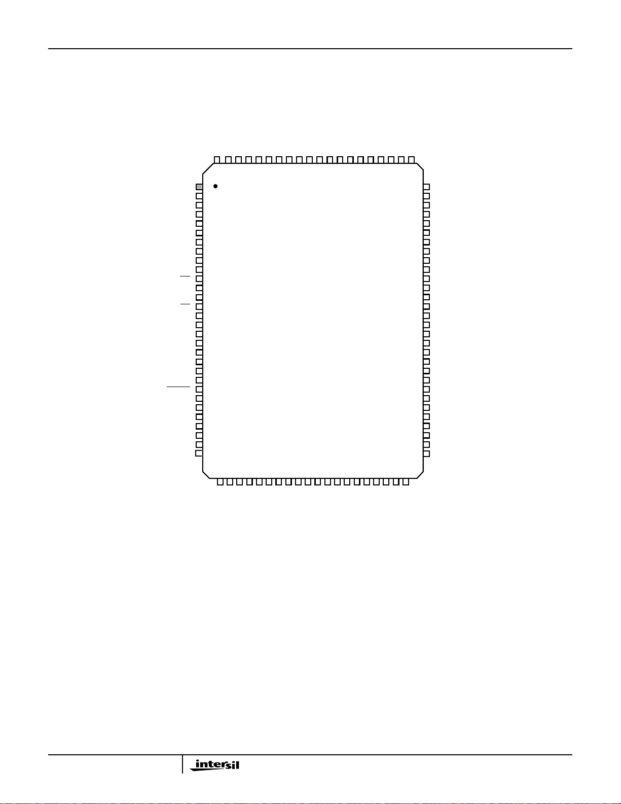
Pinout
HSP50415
100 LEAD MQFP
TOP VIEW
CDATA0
CDATA1
CDATA2
VDD
CDATA3
CDATA4
GND
CDATA5
CDATA6
CDATA7
RD
WR
GND
CE
ADDR0
ADDR1
ADDR2
REFCLK
2XSYMCLK
INTREQ
NC
VDD
RESET
CLK
GND
DVDD
DGND
PLLRC
PGND
PVDD
DIN5
VDD
DIN4
GND
DIN3
DIN2
DIN1
DIN0
DATACLK
99 98 97 96 95 94 93 91 89 87 85 84 83 818286889092100
1
2
3
4
5
6
7
8
9
10
11
12
13
14
15
16
17
18
19
20
21
22
23
24
25
26
27
28
29
30
HSP50415
DIN6
DIN7
DIN8
DIN9
DIN11
DIN10
GND
DIN12
VDD
DIN13
DIN14
80
79
78
77
76
75
74
73
72
71
70
69
68
67
66
65
64
63
62
61
60
59
58
57
56
55
54
53
52
51
DIN15
ISTRB
TXEN
LOCKDET
FOVRFL
FEMPTY
FFULL
GND
SYSCLK/2
IOUT13
VDD
IOUT12
IOUT11
IOUT10
IOUT9
IOUT8
GND
IOUT7
IOUT6
VDD
IOUT5
IOUT4
IOUT3
IOUT2
IOUT1
IOUT0
GND
VDD
RESV
RESV
4-3
32 33 34 35 36 37 38 40 42 44 46 47 48 50494543413931
DVDD
DGND
QOUTB
AVDD
AGND
QOUTA
QCOMP1
AGND
REFLO
QCOMP2
REFIO
FSADJ
AVDD
ICOMP2
ICOMP1
IOUTA
AGND
IOUTB
RESV
RESV

HSP50415
Pin Descriptions
NAME TYPE DESCRIPTION
VDD - Digital power.
GND - Digital ground.
DVDD - DAC digital power.
DGND - DAC digital ground.
AVDD - DAC analog power.
AGND - DAC analog ground.
PVDD - PLL analog power.
PGND - PLL analog ground.
PLLRC I PLL loop filter provides for the addition of less expensive RC components in place of a crystal oscillator. The
recommended values for this pin are detailed in the ‘System CLK Generation’ section.
CLK I System and DAC clock input when APLL not in use, otherwise it is the reference to the APLL.
SYSCLK/2 O Sample Clock Divided by Two. All digital output data and status pins are output from this clock. The polarity of
SYSCLK/2 may be programmed via Register 2 bit-3.
2XSYMCLK O Tristatable Symbol NCO Clock Output Multiplied by Two. The polarity of 2XSYMCLK may be programmed via
register 2 bit-15.
REFCLK I External digital PLL reference clock input.
DIN<15:0> I Data Bus. The DIN<15:0> bus loads the input data.
DATACLK I Asynchronous data clock for DIN<15:0>.
TXEN I DIN<15:0> may be optionally gated with the TXEN pin (burst mode) or input free-running as defined by register 2
bits 18-17. The polarity of TXEN may be programmed via register 2 bit-5.
ISTRB I Data samples are input as I then Q serially with the ISTRB pin active with the I sample.The polarity of ISTRBmay
be programmed via Register 2 bit-4.
CDATA<7:0> I/O µP Bidirectional DataBus. The CDATA<7:0>databus is used for loading the configuration dataand samplevectors
for modulation. CDATA7 is the MSB.
RD I µP Read control input.
WR I µP Write strobe input.
CE I Chip enable input.
ADDR<2:0> I µP AddressBus. The ADDR<2:0>bus isused for addressingthe properregisters for loadingthe configurationdata
and sample vectors for modulation. ADDR2 is the MSB.
INTREQ O TristatableActive High Interrupt RequestOutput. The INTREQ output is enabled via register 2bit-8. Register 9 bits
6-0 enable individual events for INTREQ.
RESET While the RESET input is asserted (driven low), all processing halts andthe WPM is reset. A software reset is also
available via register 10H.
IOUT<13:0> O Tristatable In-Phase Output Samples. IOUT<13:0> outputs are enabled via register 2 bit-7.
QOUT<13:0> O Tristatable Quadrature Output Samples. QOUT<13:0> outputs are enabled via register 2 bit-6. The QOUT<13:0>
outputs are not available on the MQFP package.
FEMPT,
FOVRFL,
FFULL
LOCKDET O Tristatable Status Flag of the Digital PLL. This may be used to generate an interrupt request via INTREQ.
IOUTA,
QOUTA
IOUTB,
QOUTB
O TristatableStatus Flags forFIFO Level Monitoring. These outputs are enabled viaregister 2 bits 13-11. FIFOstatus
thresholds and control are configured via register 2 bits 23-16.
The LOCKDET output is enabled via register 2 bit-10.
O Current Outputs of the Device. Full scale output current is achieved when all input bits are set to binary 1.
O ComplementaryCurrentOutputs ofthe Device. Full scaleoutput currentis achieved on thecomplementary outputs
when all input bits are set to binary 0.
4-4

HSP50415
Pin Descriptions (Continued)
NAME TYPE DESCRIPTION
ICOMP1,
QCOMP1
ICOMP2,
QCOMP2
REFLO I Reference Low Select. When the internal reference is enabled, this pin serves as the precision ground reference
REFIO I Reference voltage input if internal reference is disabled. Reference voltage output if internal reference is enabled. Use
FSADJ I Full Scale Current Adjust. Use a resistor to ground to adjust full scale output current. Full Scale Output Current =
RESV - Reserved. These pins must be floating (not connected) for proper operation.
NC - No Connection. Pins may be connected to GND, AGND, DGND or left floating.
I Compensation Pin for use in Reducing Bandwidth/Noise. Each pin should be individually decoupled to AVDDwith
a 0.1µF capacitor. To minimize crosstalk, the partwas designed so that these pins must be connected externally,
ideally directly under the device packaging. The voltage on these pins is used to drive the gates of the PMOS
devices that make up the current cells. Only the ICOMP1 pin is driven and therefore QCOMP1 needs to be
connected to ICOMP1, but de-coupled separately to minimize crosstalk.
I Compensation Pin for Internal Bias Generation. Each pin should be individually decoupled to AGND with a 0.1µF
capacitor. The voltage generated at these pins represents the voltage used to supply 2.0V nominal power to the
switch drivers. This arrangement helps to minimize clock feedthrough to the current cell transistors for reduced
glitch energy and improved spectral performance.
point for the internal voltage reference circuitry and therefore needs to have a good connection to analog ground
to enableinternal 1.2V reference.To disablethe internal reference circuitrythis pin should be connected toAVDD.
0.1µF cap to ground when internal reference is enabled.
32 x V
FSADJ/RSET
is typically 1.2V if the internal reference is used.
. Where V
is the voltage at this pin. V
FSADJ
tracks the voltage on the REFIO pin; which
FSADJ
Functional Description
The HSP50415 is a wideband programmablemodulator that
accepts an input quadrature data stream at programmable
symbol rates of up to 25MSPS (QPSK) and outputs a
modulated quadrature data stream at the final sample rate
up to 100MHz. The allowable symbol rates depend on the
modulation type selected (QPSK, 16QAM, etc.). The input
data format is parallel with respectto thebits, but serial with
respect to the I and Q samples and may be input at a
constant symbol rate or burst in at a different rate. The
HSP50415 can symbol map the input data streamper a user
programmable look up table thus allowing any standard to
be supported. The mapped symbols are then interpolated to
the finalsample rate and low-passfiltered in order to limitthe
spectral occupancy of the signal. The first stage filter
coefficients are user programmable, with subsequent filter
stages having fixed coefficients. The HSP50415 then
modulates the symbol data at the final sample rate onto a
carrier signal that is tunable from 0.023Hz - 50MHz (for a
final sample rate of 100MHz) producing a quadrature signal.
The signal may then be optionally X/SIN(X) filtered to
compensate for the SIN(X)/X roll-off of the DACs. To correct
forsystem (or DACinduced) gain imbalances between the In
phase and Quadraturesignals there is a final gain correction
stage prior to the output. The final Intermediate Frequency
(IF) digital output can be converted to differential analog
signals via the onboard 12-bit DACs or may be optionally
brought out as 14-bit digital data. The 100-pin MQFP
package provides a real digital output at 1/2 the final sample
rate.
System CLK Generation
The HSP50415 receives I and Q input data serially at twice
the input symbol rate. The data is converted to a parallel
quadrature data stream at the symbol rate by the Front End
Data Input Block. This data stream is upsampled to the final
output sample rate of the device(FSout). This output sample
rate (maximum rate of 100MHz) is used to clock the last
stage of the digital logic and the dual 12-bit DACs and may
be provided externally on the CLK pin or may be generated
by an internal analog PLL (APLL). When enabled, the APLL
uses the CLK pin as a reference and provides a selectable
CLK multiplier of x2, x4, x8, x16 or x32 or CLK divider of /2,
/4 or /8.
An external loop filter is required to be supplied at PLLRC.
The recommend configuration is shown in Figure 1, with
suggested component values calculated as:
User Input Terms:
APLLclkdivider=APLL CLK divider programmed input
APLLvcodivider=APLL VCO divider programmed input
Fclk=CLK frequency input
Fscale=loop bandwidth divisor input
Pm=loop phase margin input (degrees)
Component calculation formulas:
C1=(Fvcogain*Icp)/(wo*wo*sqrt(kk))
C2=kk*C1
R1=1/sqrt(Fvcogain*Icp*C1*sqrt(C2/C1))
Where:
Fvcogain=231000000/APLLvcodivider
Icp=0.000353
4-5

HSP50415
kk=(1+(sin(Pm*pi/180)))/(1-(sin(Pm*pi/180)))
wo=2*pi*((Fclk/APLLclkdivider)/Fscale)
A MATLAB or Excel program for calculating the component
values is available. For improved APLL performance,
utilization of specific calculated values is recommended over
the general purpose ones shown in Figure 1.
Symbol NCO
As the data flows through the device, the sample rate
increases up to the final sample rate, with the SYMBOL
NCO generating all of the necessary intermediate sample
rate clocks. Each stage’s input and output sample rate is
dependent on the interpolation rate through the stage.
Figure 1shows the various symbolclocks that are generated
on the chip. The symbol rateclock (symclk) used internally is
multiplied by 2 and output on pin 2XSYMCLK for use in
SYSCLK/2
÷2
driving the input DATACLK if a symbol rate synchronous
(non-burst) mode is required.
The SYMBOL NCO is a 32-bit accumulator. The 32-bit
frequency step (Phinc) is the sum of the user programmable
32-bit symbol Phinc and any error term generated by the
Digital Phase Lock Loop (DPLL) while locking to an external
symbol rate. The DPLL error term may be disabled by a
control bit. The symbol rates supportedare from 0.023Hz up
to 25MHz (for FSout of 100MHz) with 32-bit frequency
resolution. The formula for programming the symbol Phinc
register is given as:
symbolPhinc = (symbolRate / FSout) * 2^32
The SYMBOL NCO also has a counter mode in which the
symbol clocks are generated upon the counter reaching the
16-bit user programmable rollover count value. This mode is
useful forcases where the frequency is aninteger number of
the system clock (SYSCLK/2).
BYPASS
sysclk
APLL
SELECTOR
CLK
DIN<15:0>
INTERFACE
DATACLK
2XSYMCLK
Internal IC signal names are shown in lowercase.
DAT A
FIFO
X 2
I
CONST.
MAP
Q
INT.
FIR
I GAIN
symclk
(symbol rate) (symbol rate X 1,2,4,8,16,32)
FIGURE 1. SAMPLE RATE CLK GENERATION
HALFBAND
SYMBOL NCO
COMPLEX
DC TO 20MHz: C1=690PF, C2=11NF, R1=120Ω
20 TO 100MHz: C1=130PF, C2=2NF, R1=620Ω
MIXERFILTER
X
SIN(X)
I GAIN I OFFSET
PLLRC
C1
12-BIT
DAC
R1
C2
IOUTA
IOUTB
4-6

HSP50415
TABLE 1. HSP50415 FILTER CONFIGURATIONS AND RESULTING SYMBOL NCO RATES
BYPASS HALFBAND
BYPASS FIR FILTER FIR INTERPOLATION
0 x2 (Note) 0 Symbol Rate x 4 PhincLL x 4
0 x4 0 Symbol Rate x 8 PhincLL x 8
0 x8 0 Symbol Rate x 16 PhincLL x 16
0 x16 0 Symbol Rate x 32 PhincLL x 32
0 x2 (Note) 1 Symbol Rate x 4 PhincLL x 4
0 x4 1 Symbol Rate x 4 PhincLL x 4
0 x8 1 Symbol Rate x 8 PhincLL x 8
0 x16 1 Symbol Rate x 16 PhincLL x 16
1 Not applicable 0 Symbol Rate x 2 PhincLL x 2
1 Not applicable 1 Symbol Rate x 1 PhincLL x 1
NOTE: An optional decimate by two mode allows the device to achieve interpolation by a factor of two in the Shaping FIR.
FILTER
INTERPOLATINGFILTER
DATA INPUT RATE SYMBOL NCO PHINC
The SYMBOL NCO 32-bit Phinc value is adjusted
automatically such that the SYMBOL NCO runs at the input
rate of the interpolating filter, since this is the fastest rate
prior to the FSout rate. Table 1 lists possible filter
configurations of the HSP50415 and the resulting
interpolating filter rate. This resulting rate is affected by rate
adjustments (interpolation) in the previous filter blocks.
Digital Phase Lock Loop
The HSP50415 contains a Digital Phase Lock Loop (DPLL)
that performs symbol tracking to an external symbol clock
(REFCLK). The DPLL consists of a programmable
phase/frequency error detector followed by a loop filter and
lock detector stage. The phase/frequency error detector
block diagram is shown in Figure 2.
The DPLL uses two (integer) counters to give added
frequency programming flexibility. The programmed symbol
rates are functions of the both the REFCLK divider and the
NCO divider (N = NCO divider + 1, see Figure 2), each of
which can be changed separately. As an example, these two
counters can be set to generate a non-integer output (NCO
Symbol rate) frequency (16/3) of the input reference
frequency (REFCLK). In this case NCO divider = 16, and
REFCLK divider =3. If REFCLK is the desired symbol rate,
then the REFCLK divider will be the same value as the NCO
divider.If REFCLK isfor example2x the desired symbolrate,
then therefClk divider will be 2x the NCO divider.REFCLK is
divided down by the REFCLK divider. The internal symbol
clk is divided down by the NCO divider. When the carry-out
of the REFCLK divider is generated, the symbol NCO is
sampled. The phase and frequency (dphi/dt) should be zero
if the two rates are phase and frequency locked. If not, the
sampled phase value is the phaseError. This value is
subtracted from the previous phaseError to generate the
frequency error. Both of these error terms are input to the
loop filter which scales and integrates these error terms and
produces a final symbol nco error term. This final error term
gets addedto the SYMBOL NCO toadjust the symbol rateto
try to track to the divided down external REFCLK input. The
loop filter error term must be enabled in the software for this
error term to be added to the symbol NCO. Otherwise the
Digital PLL has no effect on the symbol rate.
The minimum value the REFCLK divider and NCO divider
values may be programmed to is the larger of 32/clkDivisor
or 0x04, where clkDivisor is FSout/REFCLKrate. This is due
to the minimum number of system clock (SYSCLK/2) cycles
the loop filter requires to process the new error terms. The
maximum rate of this clock is FSout/4 or 25MHz for FSout of
100MHz. The phaseError and freqError terms are input to
the loop filter block which is a standard lead/lag type second
order loop filter as shown in Figure 3. The loop filter requires
32 clock cycles to process a new error term.
The phaseError is weightedby the lag gain and added to the
freqError weighted by the frequency gain and this sum is
accumulated to give the integral response. The lag
accumulator is compared to upper and lower limits and
forced to the limit value if either limit isexceeded. This keeps
the SYMBOL NCO frequency within the expected symbol
rate uncertainty and limits the pull in range. This
accumulator output is then added to the phaseError
weighted by the lead gain to get a proportional response.
This lead term should be zeroed during initial tracking. The
gain values are user programmable with a mantissa and
exponent of the following format
Gain = 01.MMMM * 2^(EEEEE-17)
where MMMM denotes the 4-bit gain value and EEEEE is
the 5-bit shift value.
The phaseError and freqError signals may be monitored on
the digital outputs for test or the lock detect pin may be used
to monitor the symbol tracking phase error. The lock detect
pin indicates whether the DPLL has phase locked to the
external symbol clock. The lock detect status may also be
used to generate an interrupt event. The lock detect block
diagram is shown in Figure 4.
4-7

NCO divider<13:0>
HSP50415
REFCLK divider<7:0>
REFCLK
CLK
frequencyGain
freqError<15:0>
lagGain
phaseError<21:0>
leadGain
8-BIT
COUNTER
TC
SYNC
14-BIT
COUNTER
8 upper bits of phaseAccum14-bit countValue
enable
carryOut
R R
SYMBOL NCO
FIGURE 2. PHASE/FREQUENCY ERROR DETECTOR
UL<31:0>
LL<13:0>
41
LIMITER R R
/
FIGURE 3. DPLL LOOP FILTER
FIFOFreqError<8*7,7:0>
freqError<15:0>
_
phaseError<21:0>
DPLL
PhincError<31:0>
positive lockedValue
negative notLockedValue
threshold<20:0>
phaseErrorMag<20:0>
analogPLLlockStatus
useAPLLlockStatus
_
carryOut
AO
A1
S
FIGURE 4. LOCK DETECTION BLOCK DIAGRAM
The Lock Detector compares the magnitude of the
phaseError to a programmable 21-bit threshold value. If the
carry out from this comparison is “1” then the phaseError is
greater than or equal to the threshold value and a negative
value is added to the lock integrator. If the carry out is “0”
then the phaseError is less than the threshold and a positive
value is added. As the phaseError magnitude stays below
the threshold level the lock integrator will grow from a
negative number to a positive one thus indicating a locked
condition. The lock integrator resets to a full-scale negative
value. The sign bit of the lock integrator is output as the
LOCKDET status flag. The values added or subtracted to
the lock integrator are user selectable as follows in Table 2.
lockIntegrator<8> LOCKDET
AO
Z
Z
A1
S
bit=1 indicates phaseErr > thld so NOT
locked
R
lockIntegrator<8:0>
TABLE 2. LOCK INTEGRATOR ADDENDS
LOCK
FACTOR CARRY OUT ADDEND
BINARY
VALUE
0xx 1 -0.5 111111000
1xx 1 -0.25 111111100
x00 0 +0.0625 000000001
x01 0 +0.1250 000000010
x10 0 +0.2500 000000100
x11 0 +0.5000 000001000
4-8

HSP50415
Front-End Data Input Block
The HSP50415 accepts input data in a parallel bit fashion
with I and Q samples input serially asshown in Figure 5. The
signal pins on the device that input data to the front-end are
the DIN<15:0> bus, the ISTRB and TXEN control pins and
the DATACLK pin.
Iin<15:0>, Qin<15:0>
serial Data Stream
at symbol Rate x2
FIGURE 5. SERIAL TO PARALLEL DATA CONVERSION
FRONT END
DATA INPUT
BLOCK
All data is synchronous to the DATACLK. Further references
to bit-widths will be with respect to a single channel (I and Q
channels are identical). The input data may be from 1-bit up
to 16-bits wide with bits positioned on the LSB’s of the bus.
The data samples are input as I then Q serially with the
ISTRB pin active with the I sample. The maximum data rate
is 50MHz at FSout of 100MHz or twice the maximum symbol
rate. The data written into the chip may be gated with the
TXEN pin (burst Mode) or input free-running. The ISTRB
and TXEN pins have user-programmable active states thus
allowing spectral inversion to be implemented by simply
changing the ISTRB polarity. Figure 6 shows the input data
timing (assuming the ISTRB pin is an active high).
DATACLK
DIN<15:0>
ISTRB
FIGURE 6. I/Q INPUT DATA TIMING
I Q I Q
Once a valid pair of I and Q samples has been received, the
data pairis written into the 256x32-bit FIFO. The datais read
out of the FIFO at the symbol rate using the internally
generated symbol clock which is synchronous to the clock
pin. This internally generated symbol clock is available on
the 2XSYMCLK pin of the chip. It has been multiplied up to
twice the symbol rate to facilitate tying it to the DATACLK pin
in symbol rate synchronous modes.The data is always input
to the chip at twice the rate at which it is written to the FIFO
since Iand Q are inputserially. In asymbol rate synchronous
mode, the data is input to the front-end at twice the symbol
rate,writtento the FIFO atthe symbol rate and readfrom the
FIFO also at the symbol rate. This mode ensures that no
FIFO overflow or underflow conditions will occur. Optionally,
in a totally synchronous mode, the FIFO may be bypassed
altogether if power conservation is critical.
Reading data out of the FIFO for transmission may be
optionally gated by the TXEN pin if the user wishes to burst
the data into the chip and delay transmission of the data. If
Iout<15:0>
Qout<15:0>
at symbol rate
the data reads are not gated, then after 2 FIFO locations
have been written, data reads are initiated. Via userprogrammable bits, the data may be zeroed leaving the
front-end if the FIFO runs out of data or in gated-read mode,
if the TXEN pin is inactive. Conversely, writing data into the
FIFO may be optionally disabled upon a FIFO full condition.
Control of the starting address for the gated reads is userprogrammable where the address may be zeroed upon start
of transmission or simply incremented from where it left off
on the last transmission.
The FIFO logic contains user programmable threshold
detection (high and low thresholds) as well as full/empty
detection. There are 4 status flags available to the user for
FIFO level monitoring: FIFOOverFlow (FOVRFL), FIFOFull
(FFULL), FIFOUnderFlow,and FIFO empty (FEMPT).These
status flags may be monitored via 3 output pins: the
underflow and empty share one pin with a user selectable
function. Any one of these flags may be used to trigger an
interrupt on the INTREQ pin if the mask register for that
status bit is set. A rising edge of the status signal will set the
interrupt status register bit and cause an external interrupt if
enabled. The only way to clear the status bit and INTREQ
pin is to write a “1” to the corresponding status register bit.
Another feature of the FIFO is the adaptive symbol rate
control logic. The internal symbol rate of the device is
controlled by the digital PLL if enabled. Since the data is
read out of the FIFO at the internal symbol rate, there may
arise a needfor the FIFO toadjust the symbol rate ifthe data
is not being written in and read out at the same rate. This is
achieved by either adding or subtracting a frequency error
term to the digital PLL’s loop filter frequency term or by
forcing the loop filter lag term to its programmed limit. If a
FIFO overflow occurs, then the data is being written into the
FIFO faster than it is being read out, which indicates the
symbol rate needs to be increased thus speeding up the
reads. This scenario wouldcause the FIFO to try to increase
the final symbol rate error term by either adding the FIFO
frequency error term (user programmable) to the loop filter’s
frequency error term or force the loop filter lag accumulator
to its programmed upper limit. If a FIFO underflow occurs,
then the data is being read out of the FIFO faster than it is
being written in and the FIFO would attempt to slow down
the symbol rateby subtracting the frequency error termor by
forcing the lag accumulator to its lower limit. This adaptive
rate control is user programmable via Register 2 bits 21:20.
Constellation Mapper
The I/Q data pair from the Front End Input Block enters the
constellation mapper at the internal symbol rate and is
mapped via a user programmable look up table to new
symbol data. The symbol mapping is only supported for I/Q
bit widths of 4-bits (256-QAM) or less. The I data is
concatenated with the Q data to form the 8-bit address
(Iin<3:0>:Qin<3:0>) to the 256x8-bit RAM. The 8-bit data
output from the RAM is the new symbol data in the form
4-9
 Loading...