

Intersil Corporation HSP50306 Datasheet
HSP50306
February 1998
Features
• 25.6MHz or 26.97MHz Clock Rates
• Single Chip QPSK Demodulator with 10kHz Tracking
Loop
• Square Root of Raised Cosine (
α = 0.4) Matched
Filtering
• 2.048 MBPS Reconstructed Output Data Stream
• Bit Synchronization with 3kHz Loop Bandwidth
• Internal Equalization for Multipath Distortion
• 6-Bit Real Input: Digitized 10.7MHz or 2.1MHz IF
• Level Detection for External IF AGC Loop
• 0.1s Acquisition Time
-9
BER
•10
• <116mA on +5.0V Supply
Applications
• Cable Data Link Receivers
• Cable Control Channel Receivers
Ordering Information
TEMP.
PART NUMBER
HSP50306SC-27 0 to 70 16 Ld SOIC M16.3
HSP50306SC-2796 0 to 70 Tape and Reel
HSP50306SC-25 0 to 70 16 Ld SOIC M16.3
HSP50306SC-2596 0 to 70 Tape and Reel
RANGE (oC) PACKAGE
PKG.
NO.
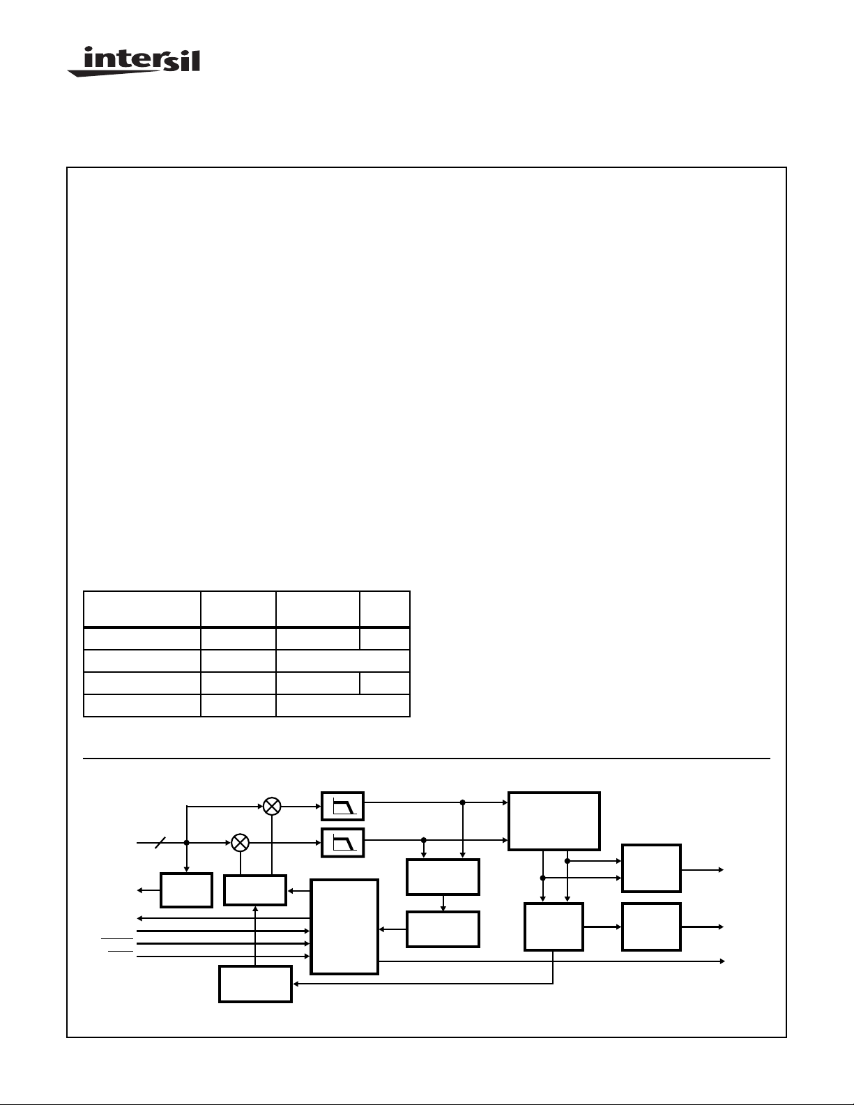
Digital QPSK Demodulator
Description
The HSP50306 is a 6-bit QPSK demodulator chip designed
for use in high signal to noise environments which have some
multipath distortion. The part recovers 2.048 MBPS data from
samples of a QPSK modulated 10.7MHz or 2.1MHz carrier.
The chip coherently demodulates the waveform, recovers
symbol timing, adaptively equalizes the signal to remove
multipath distortion, differentially decodes and multiplexes the
data decisions. 8-A lock signal is provided to indicate when
the tracking loops are locked and the data decisions are valid.
To optimize performance, a gain error feedback signal is
provided which can be filtered and used to close an I.F. AGC
loop around the A/D converter.
The QPSK demodulator derives all timing from CLKIN. The
chip divides this clock by 2 to provide the sample clock for the
external A/D converter. The -27 version operates at a clock
input of 26.97MHz and demodulates a 10.7MHz QPSK signal
to recover the 2048 KSPS data. The -25 version oper ates at a
clock input of 25.6MHz and demodulates a 2.1MHz QPSK
signal to recover the 2048 KSPS data. Variation from these
CLKIN frequencies will progressively degrade the receive
data rate, the receive IF, acquisition sweep rate, acquisition
sweep range and loop bandwidths as the deviation increases
from normal CLKIN. Details on the maximum allowable deviation are found in the Input Characteristics section. The
HSP50306 processes 6-bit offset binary data. 4-bit data provides adequate performance for many applications.
Block Diagram
I
DIN0-5
AGCOUT
ADCLK
CLKIN
RESET
TEST
CAUTION: These devices are sensitive to electrostatic discharge; follow proper IC Handling Procedures.
http://www.intersil.com or 407-727-9207
6
DETECT
LEVEL
SINCOS
NCO
TIMING
GENERATOR
CARRIER
LOOP FILTER
| Copyright © Intersil Corporation 1999
Q
BIT PHASE
DETECTOR
BIT SYNC
LOOP FILTER
8-272
4 TAP
ADAPTIVE
EQUALIZER
CARRIER
PHASE
DETECT
I
Q
DIFF.
DECODE/
MUX
LOCK
DETECT
DATAOUT
LOCK
CLKOUT
File Number 4162.2
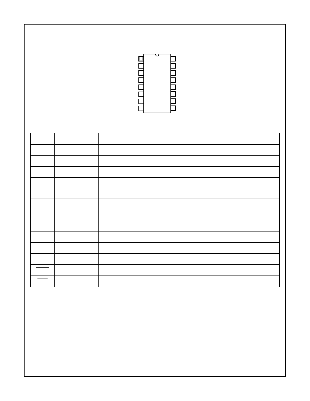
Pinout
HSP50306
16 LEAD SOIC
TOP VIEW
AGCOUT
CLKOUT
DATAOUT
LOCK
RESET
TEST
CLKIN
GND
1
2
3
4
5
6
7
8
16
15
14
13
12
11
10
9
V
CC
ADCLK
DIN0
DIN1
DIN2
DIN3
DIN4
DIN5
Pin Description
NAME SOIC PIN TYPE DESCRIPTION
V
CC
GND 8 - Ground
CLKIN 7 I Clock input. This is the processing clock for the part. All timing is derived from this clock.
DIN (5:0) 9-14 I I.F. input samples from the A/D converter. These bits interpreted as offset binary format. DIN5 is the
ADCLK 15 O This output clock is the clock for the A/D converter.
16 - +5V Power Supply
MSB. If fewer than 6 bits are used, the bits from the A/D should be connected to the MSBs of the
input and the unused LSBs grounded.
AGCOUT 1 O This output indicates whether the magnitude of the input samples are above or below the expected
level. This output is provided as an error detector for an external AGC loop. The output is low when
the input is greater than nominal, and high when the input is lower than nominal.
DATAOUT 3 O This is the recovered data.
CLKOUT 2 O This is the recovered clock.
LOCK 4 O This signal indicates that the carrier tracking loop is locked and data on the DOUT pin should be v alid.
RESET 5 I This input is provided to for initialization and test. Active low.
TEST 6 I This input is provided for test. Pull high for normal operation.
8-273
HSP50306
The Block Diagram of the QPSK Demodulator is shown on
page 1. To demodulate the data, the I.F. samples are multiplied by sine and cosine samples from a numerically controlled oscillator. The digital mixer outputs are then low pass
filtered to remove mixer products. The filtered data is then
equalized by a 4 tap equalizer (1 precursor , one ref erence tap,
and a 2 tap Decision Feedback Equalizer (DFE) to remove
distortion caused by multipath. The output of the equalizer is
differentially decoded and multiplexed into the output data
stream. The carrier tracking loop providing the L.O. f or the digital mixer is a second order digital Costas loop with a tracking
bandwidth of ~10kHz. A sweep circuit searches the carrier
uncertainty using a triangle sweep algorithm during acquisition. A lock detector controls the sweep and indicates when
valid data is available. The recovered data rate clock is generated by another numerically controlled oscillator. The timing
recovery loop is a first order decision directed digital phase
locked with a loop bandwidth of
~3kHz. The Level Detect cir-
Application Example
(25.6MHz)
26.97MHz
OSC
DIGITIZED
I.F. FILTER
10.7MHz (2.1MHz)
IF INPUT
CA3304/6
A/D
cuitry generates the AGC error signal by rectifying the I.F.
input samples and comparing them against a threshold. The
error signal is low if the signal magnitude is above the upper
threshold, high if the magnitude is below the lower limit.
Figure 1 shows the circuit of a typical demodulator
application. The typical Bit Error Rate (BER) performance is
shown in Figure 2 for both 4-bit and 6-bit quantized inputs.
The theoretical QPSK BER Perf ormance Curve is provided for
reference. Note that the BER performance shown in Figure 2
includes a multipath distortion element at the input, in addition
to the desired signal. This multipath distortion is
representative of receive signal distortions found in cable data
links.
Table 1 details the BER, Acquisition and Delay Performance
Specifications of the HSP50306 QPSK demodulator chip,
based on an input that complies with the specifications
detailed in Table 2.
HSP50306
CLKIN
6
V+
DIN0-5
ADCLK
AGCOUT
RESET TEST
CLKOUT
DATAOUT
LOCK
2.048 MBPS
OUTPUT
DATA/CLK
FIGURE 1. APPLICATIONS CIRCUIT EXAMPLE
0.01
0.001
0.0001
0.00001
1E-06
1E-07
1E-08
BIT ERROR RATE (BER)
1E-09
1E-10
1E-11
1E-12
11 12 13 14 15 16 17 18 19 20 21 22 23
NOTE: Simulation performed using alpha = 0.4 Root Raised Cosine Transmit Filtering, Multipath -10dBc at 72o at 1.6µs.
FIGURE 2. TYPICAL BIT ERROR RATE PERFORMANCE
THEORETICAL
E
6-BIT DATA
S/NO
4-BIT DATA
8-274
 Loading...