Intersil Corporation HSP50216 Datasheet
HSP50216
PRELIMINARY
Data Sheet February 2000
Four-Channel Programmable Digital
DownConverter
The HSP50216 Quad ProgrammableDigitalDownConverter
(QPDC) is designed for high dynamic range applications
such as cellular basestations where multiple channel
processing is required in a small physical space. The QPDC
combines into a single package,asetoffour channels which
include: digital mixers, a quadrature carrier NCO, digital
filters, a resampling filter, a Cartesian-to-polar coordinate
converter and an AGC loop.
The HSP50216 accepts four channels of 16-bit real digitized
IF samples which are mixed with local quadrature sinusoids.
Each channel carrier NCO frequency is setindependentlyby
the microprocessor.Theoutputofthe mixers are filtered with
a CIC and FIR filters, with a variety of decimation options.
Gain adjustment is provided on the filtered signal. The digital
AGC provides a gain adjust range of up to 96dB with
programmable thresholds and slew rates. A cartesian to
polar coordinate converter provides magnitude and phase
outputs. A frequency discriminator provides a frequency
output via the FIR filter. Selectable outputs include I
samples, Q samples, Magnitude, Phase, Frequency and
AGCgain. The output resolution is selectable from 4-bit fixed
point to 32-bit floating point.
The maximum output bandwidth achievable using a single
channel is at least 1MHz.
File Number 4557.2
Features
• Up to 70MSPS Input
• Four Independently Programmable Downconverter
Channels in a single package
• Four Parallel 16-Bit Inputs -Fixed or Floating Point Format
• 32-Bit Programmable Carrier NCO with > 115dB SFDR
• 110dB FIR Out of Band Attenuation
• Decimation from 8 to >65536
• 24-bit Internal Data Path
• Digital AGC with up to 96dB of Gain Range
• Filter Functions
- 1 to 5 Stage CIC Filter
- Halfband Decimation and Interpolation FIR Filter
- Programmable FIR Filter
- Resampling FIR Filter
• Cascadable Filtering for Additional Bandwidth
• Four Independent Serial Outputs
• 3.3V Operation
Applications
• Narrow-BandTDMA through IS-95 CDMA Digital Software
Radio and Basestation Receivers
Ordering Information
PART
NUMBER
HSP50216KI -40 to +85 196 Ld BGA V196.12x12
1
FOR MORE INFORMATION CONTACT: JUAN GARCIA - 321-729-5883
CAUTION: These devices are sensitive to electrostatic discharge; follow proper IC Handling Procedures.
TEMP
RANGE (oC) PACKAGE PKG. NO
| Copyright © Intersil Corporation 2000
Block Diagram
HSP50216
2
Pinout
HSP50216
196 LEAD BGA
TOP VIEW
12
123456789 1110
A
A5
B
A3
A6
A8
C
A1
A2
A4
D
B15 P12
E
B13 P10GND
F
B11 GND P8VCC
G
B9 VCC P6GND
H
CLK
VCC
J
B7P2GND
K
B5 GND P0VCC
L
B3
M
B1
N
C15
P
B14
A0 P13RESET
B12
ENIB RDCE
B0
C12 C6 C4 C2 C0
C14 C10 C8 GND VCC GND
A10 GNDVCC
B10
GND
B8
B6
B4 P1
VCC
SD1B
D15 D3 D1 D0
VCC
ENIC
SCLK SYNCCSYNCBSYNCA SYNCD SYNCI SYNCOA7 A9 A11 A13 A15 SD1A
SD2C SD2DSD2B
SD1CGNDVCCGND ADD0
ADD2
µP MODE
ENIDD13
D11
VCC D9GND
D12 D10D14C13
SD1D
INTRPT P15ENIA A12 A14 SD2A
P9
P7
P5
D7
D8 D6 D4C11 C9 C7 C5 C3 C1
13 14
ADD1
P14
VCCP11
GND P4
VCCP3
WRB2
D5 D2
POWER PIN
GROUND PIN
3
SIGNAL PIN
THERMAL BALL
NC (NO CONNECTION)
HSP50216
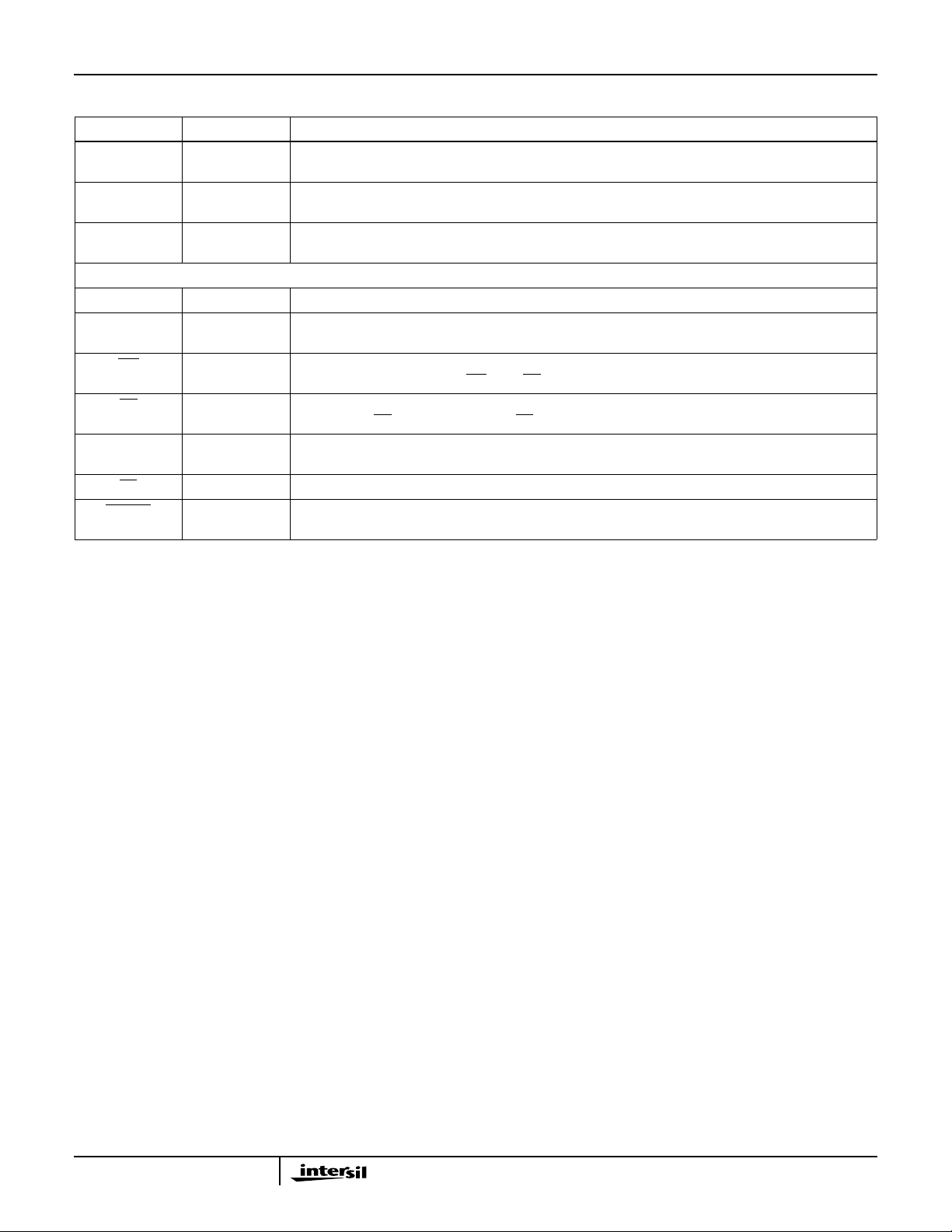
Pin Descriptions
NAME TYPE DESCRIPTION
POWER SUPPLY
VCC - Positive Power Supply Voltage, 3.3V ±0.15
GND - Ground, 0V.
INPUTS
A(15:0) I Parallel Data Input bus A. Sampled on the rising edge of clock when ENIA is active (low).
B(15:0) I Parallel Data Input bus B. Sampled on the rising edge of clock whenENIB is active (low).
C(15:0) I Parallel Data Input bus C. Sampled on the rising edge of clock when ENIC is active (low).
D(15:0) I Parallel Data Input bus D. Sampled on the rising edge of clock when ENID is active (low).
ENIA I Input enable for Parallel Data Input bus A. Active low. This pin enables the input to the part in one of two
modes, gated or interpolated. In gated mode, one sample is taken per CLK when ENI is asserted.
ENIB I Input enable for Parallel Data Input bus B. Active low. This pin enables the input to the part in one of two
modes, gated or interpolated. In gated mode, one sample is taken per CLK when ENI is asserted.
ENIC I Input enable for Parallel Data Input bus C. Active low. This pin enables the input to the part in one of two
modes, gated or interpolated. In gated mode, one sample is taken per CLK when ENI is asserted.
ENID I Input enable for Parallel Data Input bus D. Active low. This pin enables the input to the part in one of two
modes, gated or interpolated. In gated mode, one sample is taken per CLK when ENI is asserted.
CONTROL
CLK I Input clock. All processing in the HSP50216 occurs on the rising edge of CLK.
SYNCI I Synchronization Input Signal. Used to align the processing with an external event or with other HSP50216
devices. SYNCI can update the carrier NCO, reset decimation counters, restart the filter compute engine,
and restart the output section among other functions. For most of the functional blocks, the response to
SYNCI is programmable and can be enabled or disabled.
SYNCO O Synchronization Output Signal. The processing of multiple HSP50216 devices can be synchronized by
tying the SYNCO from one HSP50216 device (the master) to the SYNCI of all the HSP50216 devices (the
master and slaves).
RESET I Reset Signal. Active low. Asserting reset will halt all processing and set certain registers to default values.
OUTPUTS
SD1A O Serial Data Output 1A. A serial data stream output which can be programmed to consist of I1, Q1, I2, Q2,
magnitude, phase, frequency (dφ/dt), AGC gain, and/or zeros. In addition, data outputs from Channels 0,
1, 2 and 3 can be multiplexed into a common serial output data stream. Information can be sequenced in
a programmable order. See Serial Data Output Formatter Section and Microprocessor Interface Section.
SD2A O Serial Data Output 2A. This output is provided as an auxiliary output forSerial Data Output 1A to route data
to a second destination or to output two words at a time for higher sample rates. SD2A has the same
programmability as SD1A except that floating point format is not available. See Serial Data Output
Formatter Section and Microprocessor Interface Section.
SD1B O Serial Data Output 1B. See description for SD1A.
SD2B O Serial Data Output 2B. See description for SD2A.
SD1C O Serial Data Output 1C. See description for SD1A.
SD2C O Serial Data Output 2C. See description for SD2A.
SD1D O Serial Data Output 1D. See description for SD1A.
SD2D O Serial Data Output 2D. See description for SD2A.
SCLK O Serial Output Clock. Can be programmed to be at 1, 1/2, 1/4, 1/8, or 1/16 times the clock frequency. The
polarity of SCLK is programmable.
SYNCA O Serial Data Output 1A sync signal. This signal is used to indicate the start of a data word and/or frame of
data. The polarity and position of SYNCA is programmable.
4
HSP50216
Pin Descriptions (Continued)
NAME TYPE DESCRIPTION
SYNCB O Serial Data Output 1B sync signal. This signal is used to indicate the start of a data word and/or frame of
data. The polarity and position of SYNCB is programmable.
SYNCC O Serial Data Output 1C sync signal. This signal is used to indicate the start of a data word and/or frame of
data. The polarity and position of SYNCC is programmable.
SYNCD O Serial Data Output 1D sync signal. This signal is used to indicate the start of a data word and/or frame of
data. The polarity and position of SYNCD is programmable.
MICROPROCESSOR INTERFACE
P(15:0) I/O Microprocessor Interface Data bus. See Microprocessor Interface Section. P15 is the MSB.
ADD(2:0) I Microprocessor Interface Address bus. ADD2 is the MSB. See Microprocessor Interface Section. Note:
ADD2 is not used but designated for future expansion.
WR I Microprocessor Interface Write Signal. The data on P(15:0) is written to the destination selected by
ADD(2:0) on the rising edge of WR when CE is asserted (low). See Microprocessor Interface Section.
RD I Microprocessor Interface Read Strobe. The data at the address selected by ADD(2:0) is placed on
P(15:0) when RD is asserted (low) and CE is asserted (low). See Microprocessor Interface Section.
µP MODE I Microprocessor Interface Mode Control. This pin is used to select the Read/Write mode for the
Microprocessor Interface.
CE I Microprocessor Interface Chip Select. Active low. This pin has the same timing as the address pins.
INTRPT O Microprocessor Interrupt Signal. Asserted for a programmable number of clock cycles when new data is
available on the selected Channel.
Functional Description
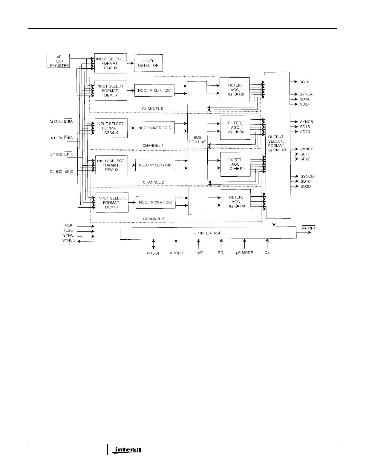
The HSP50216 is a four channel digital receiver integrated
circuit offering exceptional dynamic range and flexibility.
Each of the four channels consists of a front-end NCO/digital
mixer/CIC-filter block and a back-end FIR/AGC/polarconversion block. The parameters for the four channels are
independently programmable. Four parallel data input
busses (A(15:0), B(15:0), C(15:0) and D(15:0)) and four
serial data outputs (SDxA, SDxB, SDxC, and SDxD; x = 1 or
2) are provided. Each input can be connected to any or all of
the internal signal processing channels, Channels 0, 1, 2
and 3. The output of each channel can be routed to any of
the serial outputs. Outputs from more than one channel can
be multiplexed through a common output if the channels are
synchronized. The four channels share a common input
clock and a common serial output clock, but the output
sample rates can be synchronous or asynchronous. Bus
multiplexers between the front end and back end sections
provide flexible routing between channels for cascading
back-end filters or for routing one front end to multiple back
ends for polyphase filtering (to provide wider bandwidth
filtering). A level detector is provided to monitor the signal
level on any of the parallel data input busses.
Each front end NCO/digital mixer/CIC filter section includes
a quadrature numerically controlled oscillator (NCO), digital
mixer, and a cascaded-integrator-comb filter (CIC). The
NCO has a 32-bit frequency control word for 16.3MHz tuning
resolution at an input sample rate of 70MSPS. The SFDR of
the NCO is >115dB. The CIC filter order is programmable
between 1 and 5 and the CIC decimation factor can be
programmed from 4 to 65536, depending on the number of
stages selected.
Each back end section includes an FIR processing block, an
AGC and a cartesian-to-polar coordinate converter. The FIR
processing block is a flexible filter compute engine that can
compute a single FIR or a set of filters. A single filter in a
chain can have up to 256 taps and the total number of taps
in a set of filters can be up to 384. The filter compute engine
supports a variety of filter types including decimation,
interpolation and resampling filters. The coefficients for the
programmabledigital filters are 22 bits wide. Coefficients are
provided in ROM for several halfband filter responses and for
a resampler. The AGC section can provide up to 96dB of
either fixed or automatic gain control. For automatic gain
control, two settling modes and two sets of loop gains are
provided. Separate attack and decay slew rates are provided
for each loop gain. Programmable limits allow the user to
select a gain range less than 96dB. The outputs of the
cartesian-to-polar coordinate conversion block, used by the
AGC loop, are also provided as outputs to the user for
demodulation.
The HSP50216 supports both fixed and floating point
parallel data input modes. The floating point modes support
gain ranging A/D converters. Gated, interpolated and
multiplexeddata input modes are supported. The serial data
output word width for each data type can be programmed to
one of ten output bit widths from 4-bit fixed point through 32bit IEEE floating point.
5
HSP50216
The HSP50216 is programmed through a 16-bit
microprocessor interface. The output data can also be read
via the microprocessor interface for all channels that are
synchronized. The HSP50216 is specified to operate to a
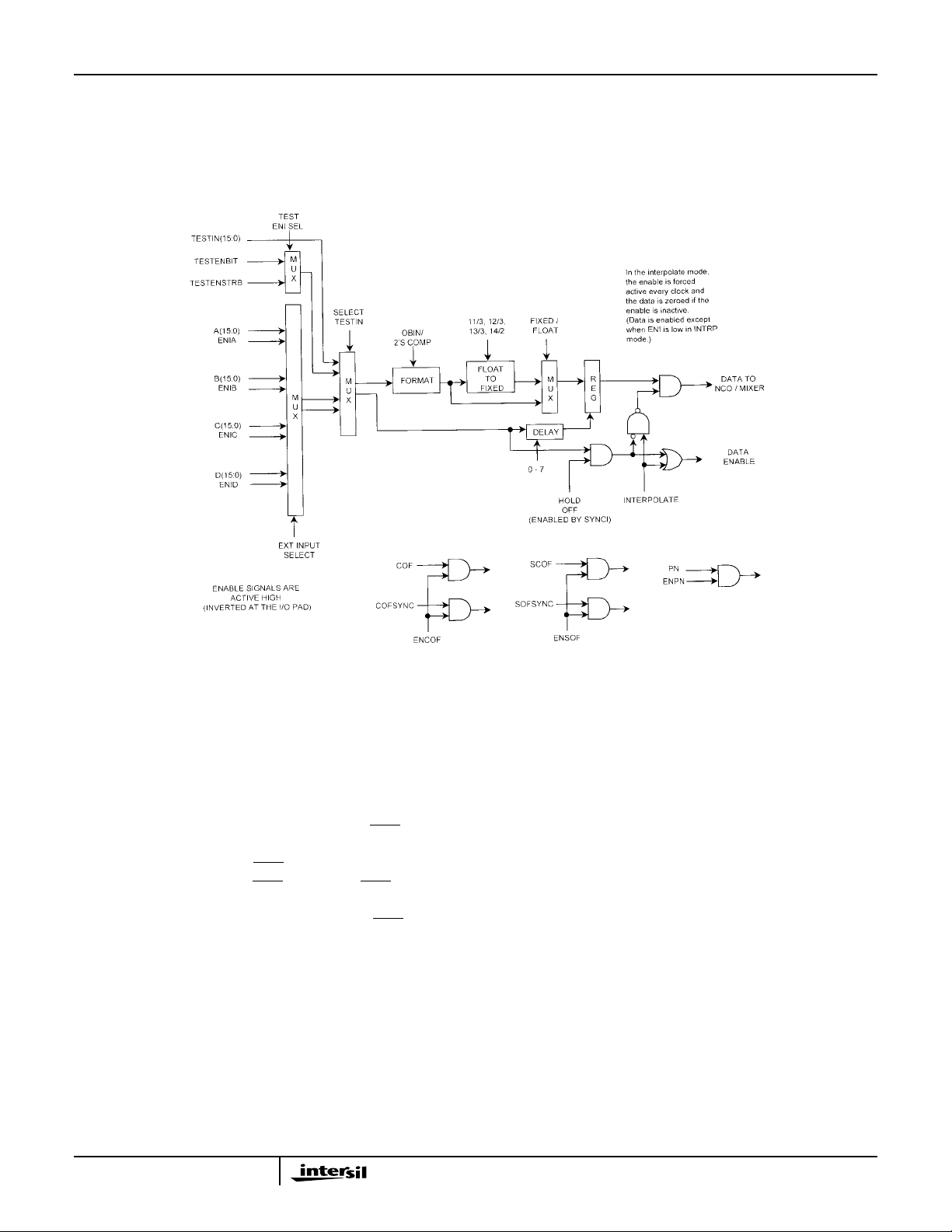
Input Select/Format Block
maximum clock rate of 70MSPS over the industrial
temperature range (-40
voltage range is 3.3V ± 0.15V. The I/Os are not 5V tolerant.
o
C to 85oC). The power supply
Each front end block and the leveldetector block contains an
input select/format block. A functional block diagram is
provided in the above figure. The input source can be any of
the four parallel input busses (see Microprocessor Interface
Section Table 1, IWA *000h) or a test register loaded via the
processor bus (see Microprocessor Interface Section Table
40, GWA F807h).
The input to the part can operate in a gated or interpolated
mode. Each input channel has an input enable (
B, C or D). In the gated mode, one input sample is
processed per clock that the
Processing is disabled when
pipelined through the part to minimize delay (latency). In the
interpolated mode, the input is zeroed when the
is high, but processing inside the part continues. This mode
inserts zeros between the data samples, interpolating the
input data stream up to the clock rate. On reset, the part is
set to gated mode and the input enables are disabled. The
inputs are enabled by the first SYNCI signal.
The input section can select one channel from a multiplexed
data stream of up to 8 channels. The input enable is delayed
by 0 to 7 clock cycles to enable a selection register. The
register following the selection register is enabled by the
non-delayed input enable to realign the processing of the
ENIx signal is asserted (low).
ENIx is high. The ENIx signal is
ENIx, x = A,
ENIx signal
channels. The one-clock-wide input enable must align with
the data for the first channel. The desired channel is then
selected by programming the delay. A delay of zero selects
the first channel, a delay of 1 selects the second, etc.
The parallel input busses are 16 bits wide. The input format
may be twos complement or offset binary format. A floating
point mode is also supported. The floating point modes and
the mapping of the parallel 16-bit input format is discussed
below.
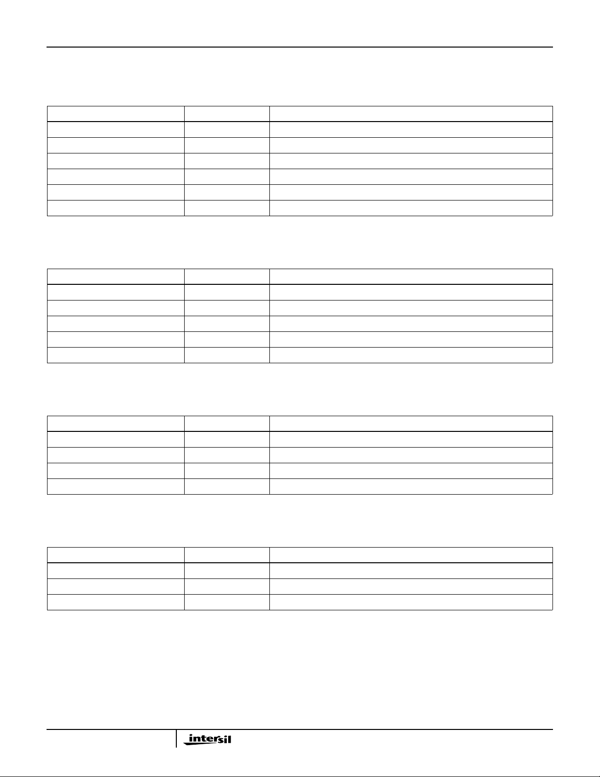
Floating Point Input Mode Bit Mapping
The input bit weighting for fixed point is 20(corresponding to
parallel input bus A, B, C or D bit 15) to 2
to parallel input bus A, B, C or D bit 0). For floating point
modes, the least significant 2 or 3 bits are used as exponent
bits (See Floating Point Input Mode Bit Mapping Tables). The
difference between the four floating point modes with three
exponent bits is where the exponent saturates.
-15
(corresponding
6
HSP50216
Floating Point Input Mode Bit Mapping Tables
A, B, C or D(15:0) Input: 2^ - 0 1 2 3 4 5 6 7 8 9 10 11 12 13(exp2) 14(exp1) 15(exp0)
11-BIT MODE: 11-BIT MANTISSA (MINIMUM), 3-BIT EXPONENT, 30dB EXPONENT RANGE
EXPONENT GAIN (dB) PIN BIT WEIGHTING TO 16-BIT INPUT MAPPING, 2^-
000 0 00000012345678910
001 6 000001234567891011
010 12 0000123456789101112
011 18 000123456789101112z
100 24 00123456789101112zz
101 (Note 1) 30 0123456789101112zzz
NOTE:
1. Or 110 or 111, the exponent input saturates at 101.
12-BIT MODE: 12-BIT MANTISSA, 3-BIT EXPONENT, 24dB EXPONENT RANGE
EXPONENT GAIN (dB) PIN BIT WEIGHTING TO 16-BIT INPUT MAPPING, 2^-
000 0 000001234567891011
001 6 0000123456789101112
010 12 000123456789101112z
011 18 00123456789101112zz
100 (Note 2) 24 0123456789101112zzz
NOTE:
2. Or 101, 110, or 111, the exponent input saturates at 100.
13-BIT MODE: 13-BIT MANTISSA, 3-BIT EXPONENT, 18dB EXPONENT RANGE
EXPONENT GAIN (dB) PIN BIT WEIGHTING TO 16-BIT INPUT MAPPING, 2^-
000 0 0000123456789101112
001 6 000123456789101112z
010 12 00123456789101112zz
011 (Note 3) 18 0123456789101112zzz
NOTE:
3. Or 100, 101, 110, or 111, the exponent input saturates at 011.
14-BIT MODE: 14-BIT MANTISSA, 2-BIT EXPONENT, 12dB EXPONENT RANGE
EXPONENT GAIN (dB) PIN BIT WEIGHTING TO 16-BIT INPUT MAPPING, 2^-
00 0 00012345678910111213
01 6 0012345678910111213z
10 (Note 4) 12 012345678910111213zz
NOTE:
4. Or 11, the exponent input saturates at 10.
7

HSP50216
Level Detector
An input level detector is provided to monitor the signal level
on any of the input busses. Which input bus, the input format,
and the level detection type are progr ammable (see
Microprocessor Interface Section Tables 37, 38 and 39,
GWA’s F804h, F805h and F806h). The supported monitoring
modes are: integrated magnitude (like the HSP50214 w/o the
threshold), leaky integration (Y
n=Xn
xA+Y
x (1-A)), and
n-1
peak detection. The measurement interval can be
programmed from 2 to 65537 samples (or continuous for the
leaky integrator and peak detect cases). The output is 32 bits
and is read via the µP interface.
NCO/Mixer
After the input select/format section, the samples are
multiplied by quadrature sine wave samples from the carrier
NCO. The NCO has a 32-bit frequency control, providing
sub-hertz resolution at the maximum clock rate. The
quadrature sinusoids have exceptional purity. The purity of
the NCO should not be the determining factor for the
receiver dynamic range performance. The phase
quantization to the sine/cosine generator is 24 bits and the
amplitude quantization is 19 bits.
The carrier NCO center frequency is loaded via the µP bus.
The center frequency control is double buffered - the input is
loaded into a center frequency holding register via the µP
interface. The data is then transf erred from the holding register
to the active register by a write to a address IW A *006h or b y a
SYNCI signal, if loading via SYNCI is enabled. To synchronize
multiple channels, the carrier NCO phase accumulator
feedbackcan be zeroed on loading to restart all of the NCOs at
the same phase. A serial offset frequency input is also available
for each channel through the D(15:0) parallel data input bus (if
that bus is not needed for data input). This is legacy support for
HSP50210 type tracking signals.
After the mixers, a PN signal can be added to the data. This
feature is provided f or test and to digitally reduce the input
sensitivity and adjust the receiver range (sensitivity). The effect
is the same as increasing the noise figure of the receiver ,
reducing its sensitivity and overall dynamic range . The one bit
PN data is scaled by a 16-bit programmable scale f actor. The
overall range f or the PN is 0 to 1/8 full scale . A gain of 0
disables the PN input. The bit weighting for the gain is:
SIGNAL (2^-):
01234567891011121314151617181920
PN (2^):
SSSXXXXXXXX X X XXXXXX
GAIN REG (2^):
XXXXXXXXXXX X X X X X
(A POSITIVE 16-BIT VALUE IS LOADED, S = SIGN)
The minimum, non-zero, PN value is 1/(2
(-108dBFS) on each axis (-105dBFS total). For an input
noise level of -75dBFS, this allows the SNR to be decreased
18
) of full scale
in steps of 1/8dB or less. The I and Q PN codes are offset in
time to decorrelate them. The PN code is selected and
enabled in the test control register (F800h). The PN is added
to the signal after the mix as:
Bit
Weights
Input Bits X XXXXXXXXXXXXXXXXXXX
PN Value± 0 00PPPPPPPPPPPPPPPP
0. 1234567890123456789
so the maximum level is -12dBFS and the minimum, nonzero level is -108dBFS. The PN code can be 2
15
2
-1 * 223-1.
15
-1, 223-1 or
CIC Filter
Next, the signal is filtered by a cascaded integrator/comb
(CIC) filter. A CIC filter is an efficient architecture for
decimation filtering. The power or magnitude squared
frequency response of the CIC filter is given by:
πMf()sin
πf
---- -
R
2N
----------------------- -
=
Pf()
sin
where
M = Number of delays (1 for the HSP50216)
N = Number of stages
and R = Decimation factor.
The CIC filter order is programmable from 0 to 5. The
minimum decimation is 4. If the order is set to 0, there must
be at least 4 clocks between samples or the decimation
counter must be set to 4 to chose every 4th sample. The
integrator/comb bit widths are:
69, 62, 53, 44, 34, 32, 32, 32, 32, 32.
The integrators are sized for decimation factors up to 512
with 5 stages. The maximum decimation varies with the
number of stages, but the maximum is 65536, limited by the
decimation counter.
A CIC filter has a gain of R
N
, where R is the decimation factor
and N is the number of stages. For a 5 stage CIC , the gain is
5
R
. The number of input bits is 24. The decimation factors that
a CIC can handle depends on the sizes of the integrators. The
integrators are sized to prev ent more than one rollo v er per
decimation period. In the HSP50216, the integrators are slightly
oversized to reduce the quantization noise at each stage.
Because the CIC filter gain can vary greatly with decimation,
a barrel shifter is provided ahead of the CIC to add gain to
the input signal. The shift factor is adjusted to keep the total
barrel shifter and CIC filter between 0.5 and 1.0. The shift
8
HSP50216
factor can be from 0 to 31. The equation used to compute
the shift factor is:
Shift Factor = 45 - Ceiling(log
(RN)).
2
NOTE: With a CIC order of zero, the CIC shifter does not have
sufficient range to route more than 10 bits to the back end.
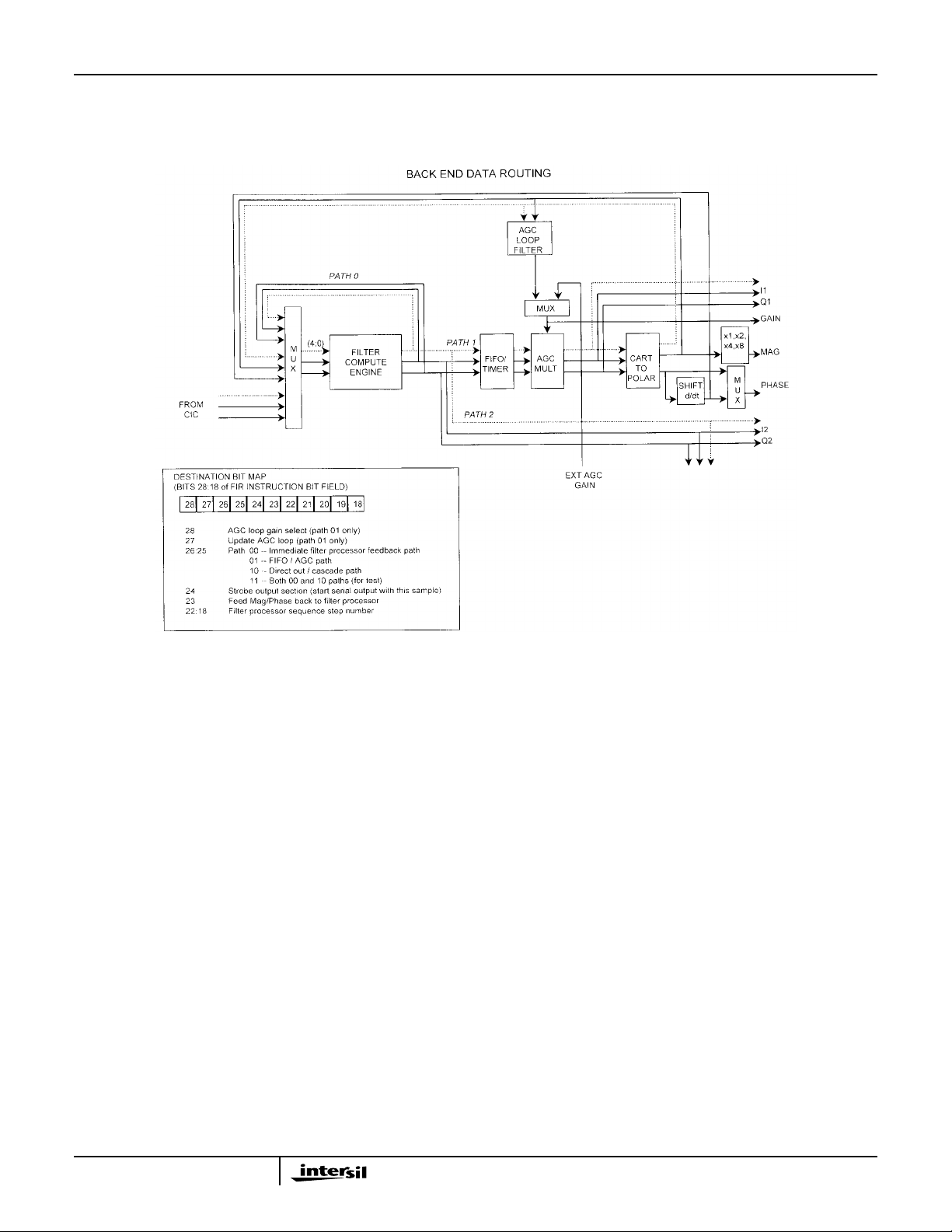
Back End Section
One back-end processing section is provided per channel.
Each back end section consists of a filter compute engine, a
FIFO for rate smoothing, an AGC and a cartesian-to-polar
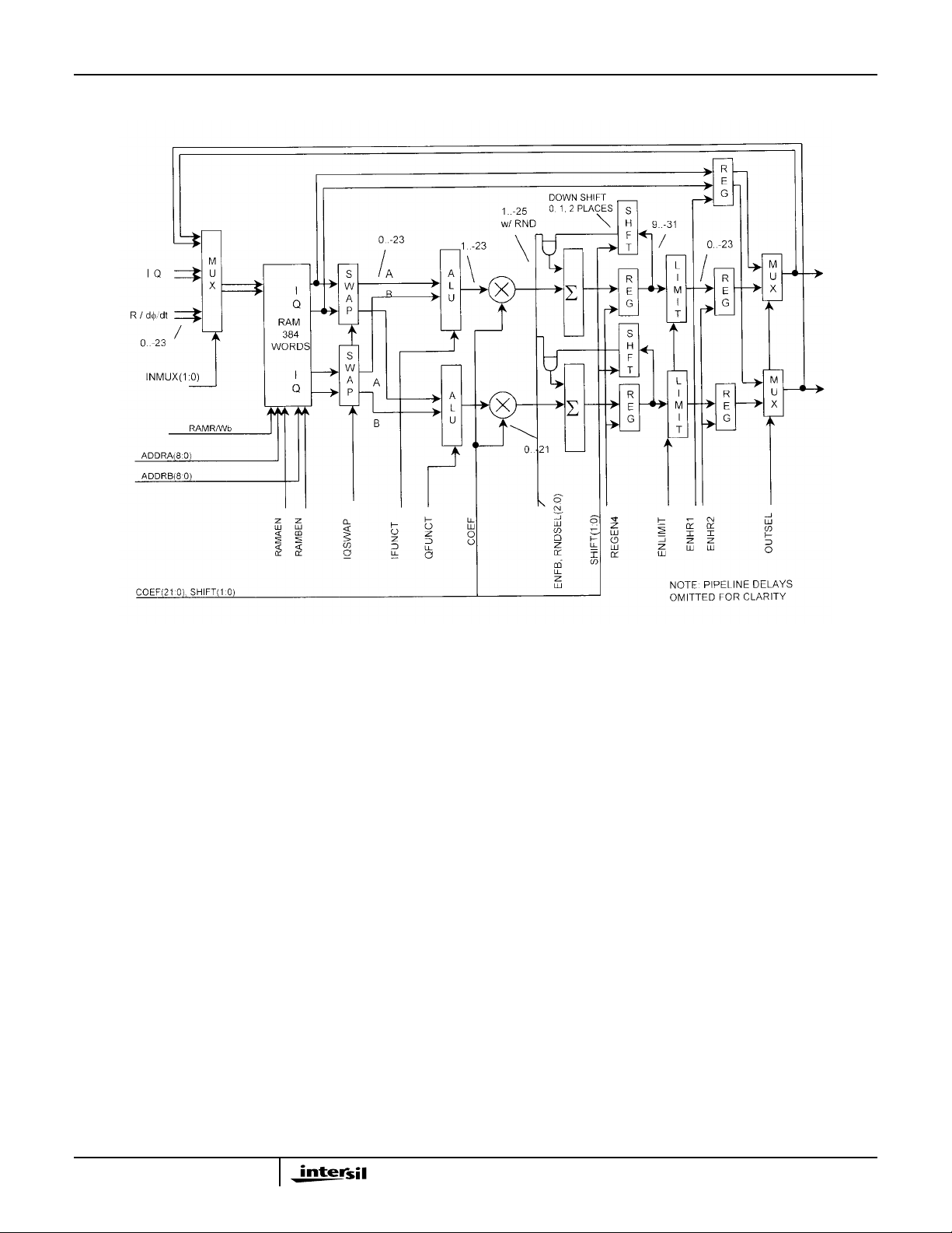
coordinate conversion block. A block diagram showing the
major functional blocks and data routing is shown above.
The data input to the back end section is through the filter
compute engine. There are two other inputs to the filter
compute engine, they are a data recirculation path for
cascading filters and a magnitude and dφ/dt feedback path
for AM and FM filtering. There are seven outputs from each
back end processing section. These are I and Q directly out
of the filter compute engine (I2, Q2), I and Q passed through
the FIFO and AGC multipliers (I1, Q1), magnitude (MAG),
phase (or dφ/dt), and the AGC gain control value (GAIN).
The I2/Q2 outputs are used when cascading back end
stages. The routing of signals within the back end
processing section is controlled by the filter compute engine.
The routing information is embedded in the instruction bit
fields used to define the digital filter being implemented in
the filter compute engine.
9
Filter Compute Engine
HSP50216
The filter compute engine is a dual multiply-accumulator
(MAC)data path with a microcoded FIR sequencer. The filter
compute engine can implement a single FIR or a set of
filters. For example, the filter chain could include two
halfband filters, a shaping (matched) filter and a resampling
filter.The following filter types are currently supported by the
architecture and microcode:
• even symmetric w/ even # of taps decimation filters
• even symmetric w/ odd # of taps decimation filters
(including HBFs)
• odd symmetric w/ even # of taps decimation filters
• odd symmetric w/ odd # of taps decimation filters
• asymmetric decimation filters
• complex filters
• interpolation filters (up to interpolate by 4)
• interpolation halfband filters
• resampling filters (under NCO control)
• fixed resampling ratio filter (within the availablenumber
of coefficients)
• quadrature to real filtering (w/ fs/4 up conversion)
The input to the filter compute engine comes from one of
three sources - a CIC filter output (which can also be another
backendsection), the output of the filter compute engine (fed
back to the input) or the magnitude and dφ/dt fed back from
the cartesian-to-polar coordinate converter.
The number and size of the filters in the chain is limited by
the number of clock cycles available and by the data and
coefficient RAM/ROM resources. The data RAM is 384
words (I/Q pairs) deep. The data addressing is modulo in
power-of-2 blocks, so the maximum filter size is 256. The
block size and the block starting memory address for each
filter is programmable so that the available memory can be
used efficiently. The coefficient RAM is 192 words deep. It is
half the size of the data memory because filter coefficients
are typically symmetric. ROMs are provided with halfband
filter coefficients, resampling filter coefficients, and
constants. The filter compute engine exploits symmetry
where possible so that each MAC can compute two filter
taps per clock, by doing a pre-add before multiplying. In the
case of halfband filters, the zero-valued coefficients are
skipped for extra efficiency. There is an overhead of one
clock cycle per input sample for each filter in the chain (for
writing the data into the data RAM) and (except in special
cases) a two clock cycle overhead for the entire chain for
program flow control instructions.
The output of the filter compute engine is routed through a
FIFO in the main output path. The FIFO is provided to more
evenly space the FIR outputs when they are produced in
10

HSP50216
bursts (as when computing interpolation filters). The FIFO is
four samples deep. The FIFO is loaded by the output of the
filter when that path is selected. It is unloaded by a counter.
The spacing of the output samples is specified in clock
periods. The spacing can be from 1 (fall through) to 4096
samples (approximately the spacing for a 16KSPS output
sample rate when using 65MSPS clock).
The number and order of the filtering in the filter chain is
defined by a FIR control program. The FIR control program
is a sequence of up to 32 instruction words. Each instruction
word can be a filter or program flow instruction. The filter
instruction defines a FIR in the chain, specifying the type of
FIR, number of taps, decimation, memory allocation, etc. For
program flow, a wait for input sample(s) instruction, a loop
counter load, and several jumps (conditional and
unconditional) are provided.
The simplest filter program computes a single filter. It has
three instructions (see Sample Filter #1Program Instructions
below):
SAMPLE FILTER #1 PROGRAM
STEP INSTRUCTION
0 Wait for enough input samples
(equal to the decimation factor)
1 FIR
Type = even symmetric
95 taps
Dec x 2
Compute one output
Decrement wait counter
Memory block size 128
Memory block start at 64,
Coefficient block start at 64
Step size 1
Output to AGC
2 Jump, Unconditional, to step 0
The parameters of the FIR (including type, number of taps,
decimation and memory usage) are specified in the bit fields
of the step 2 instruction word. To change the filtering the only
other change needed is the number of samples in the wait
threshold register. The filter in this example requires 52 clock
cycles to compute, allocated as follows:
SAMPLE FILTER #1 CLOCK CYCLES CALCULATION
CLOCK
CYCLES FUNCTION PERFORMED
48 Clocks for FIR computation (two taps/clock due to
symmetry)
2 Clocks for writing the input data into the data RAMs
(Decimate by 2 requires 2 inputs per output)
2 Clocks for the program flow instructions (wait and
jump)
52 Total
Using a 65MSPS clock, the output sample rate could be as
high as 1.25MSPS. The input sample rate from the CIC filter
would be 2.5MSPS. The impulse response length would be
38 µsec (95 taps at 0.4µs/tap).
Each additional filter added to the signal processing chain
requires one instruction step.As an example of this, a typical
filter chain might consist of two decimate-by-2 halfband
filters being followed by a shaping filter with the final filter
being a resampling filter. The program for this case might be
(see Sample Filter Program #2 Instructions below):
SAMPLE FILTER #2 PROGRAM
STEP INSTRUCTION
0 Wait for enough input samples (usually equal to the
total decimation - 8 in this case)
1 FIR
Type = even symmetry
15 taps
Halfband
Dec x 2
Compute four outputs
Memory block size 32
Memory block start at 0
Coefficient block start at 13
Output to step 2
Decrement wait count
2 FIR
Type = even symmetry
23 taps
Halfband
Dec x 2
Compute two outputs
Memory block size 32
Memory block start at 32
Coefficient block start at 24
Output to step 3
3 FIR
Type = even symmetry
95 taps
Dec x 2
Compute one output
Memory block size 128
Memory block start at 64
Coefficient block start at 64
Step size 1
Output to step 4
4 FIR
Type = resampler
Increment NCO
6 taps
Compute one output
Memory block size 8
Memory block starts at 192
Coefficient block start at 512
Step size 32
Output to AGC
5 Jump, Unconditional, to 0
11

HSP50216
Sample filter #2 requires:
• 32 + 32 + 128 + 8 = 200 data RAM locations
• (95+1)/2=48 coefficient RAM location (resampler and
HBF coefficient are in ROM).
The number of clock cycles required to compute an output
for Sample filter #2 is calculated as follows:
SAMPLE FILTER #2 CLOCK CYCLES CALCULATION
CLOCK
CYCLES FUNCTION PERFORMED
20 Halfband 1 compute clocks
(5 per compute x4 computes)
8 Halfband 1 input sample writes
14 Halfband 2 compute clocks
(7 per compute x2 computes)
4 Halfband 2 input sample writes
48 48 x 1 FIR compute clocks
2 FIR input sample writes
6 6 x 1 resampler compute clocks
1 Resampler input sample writes
1 Jump instruction
1 Wait instruction
105 Clock cycles per output
Total decimation is 8, so the input sample rate for the FIR
chain could be up to:
f
/(ceil(105/8)) = f
CLK
CLK
/14.
With a 65MHz clock, this would support a maximum input
sample rate to the FIR processor of 4.6MHz and an output
sample rate up to 0.580MHz. The shaping filter impulse
response length would be:
(95 x 2)/580,000 = 82µs.
The maximum output sample rate is dependent on the
length and number of FIRs and their decimation factors.
Illustrating this concept with Filter Example #3, a higher
speed filter chain might be comprised of one decimate-by-2
halfband filter (15 taps) followed by a 30 tap shaping FIR
filter with no decimation. The program for this example could
be:
SAMPLE FILTER #3 PROGRAM
STEP INSTRUCTION
0 Wait for enough input samples (2 in this case)
1 FIR
Type = even symmetry
19 taps
Halfband
Dec x 2
Compute one output
Memory block size 32
Memory block start at 0
Coefficient block start at 18
Output to step 2
Reset wait count
2 FIR
Type = even symmetry
30 taps
Dec x 1
Compute one output
Memory block size 64
Memory block start at 32
Coefficient block start at 64
Step size 1
Output to AGC
3 Jump, Unconditional, to 0
The number of clock cycles required to compute an output
for Sample filter #3 is calculated as follows:
SAMPLE FILTER #3 CLOCK CYCLES CALCULATION
CLOCK
CYCLES FUNCTION PERFORMED
6 6 x 1 HBF compute clocks
2 HBF input writes
15 15 x 1 FIR compute clocks
1 1 FIR input write
1 1 wait
1 1 jump
26 Clock cycles per output
For Filter Example #3 and a 65MSPS input, the maximum
output sample rate would be 2.5MSPS and the maximum
FIR processor input sample rate would be 5MSPS (At
80MSPS, the FIR could be up to 42 taps).
Channels 0, 1, 2 and 3 can be combined in a polyphase
structure for increased bandwidth or improved filtering.
12
Filter Example #4 will be used to demonstrate this capability.
Symbol rate of 4.096 MSym. The desired output sample rate
is 8.192MSPS. Arrange the four back end sections as four
filters operating on the same CIC output at a rate of
65.536MHz/4=16.384MHz.
Each channel computes the same sequence, offset by one
output sample from the previous sample. Each channel
decimates down to 2.048M and then the channels are
HSP50216
multiplexed together to get the desired 8.192MSPS. The
input sample rate to the final filter of each channel must
meet Nyquist for the final output to assure that no
information is lost due to aliasing.
SAMPLE FILTER #4 PROGRAM
STEP INSTRUCTION
0 Wait for enough input samples (8 in this case)
1 FIR
type = even symmetry
44 taps
decx8
compute one output
memory block size 64
memory block start at 0
coefficient block start at 64
step size 1
output to AGC
offset memory read pointers by 0, -2, -4, -6
2 Jump, Unconditional, to 0
The number of FIR taps available for these requirements is
calculated as follows:
65536/2048 = 32 clocks
minus (8writes + 1wait + 1jump = 10clocks)
= 22 clocks
Therefore, the number of taps is:
22 x 2 = 44 taps.
Multiplexing the four outputs gives a final output sample rate
of 8.192.
The impulse response is 44 taps at 16.384M or 22 output
samples (11 symbols at 4.096M).
The AGC loop filter output of channel 4 can be routed to
control the forward AGC gain control of all four channels.
This assures that the gains of the four back end sections are
the same. The gain error, however, is only computed from
every fourth output sample.
The back end processing sections of two or more HSP50216s
can be combined using the same polyphase approach, but
the AGC gain from one part cannot be shared with another
part (except via the µP interface), so polyphase filter using
multiple parts would typically usually use a fixed gain.
Filter Sequencer
13

HSP50216
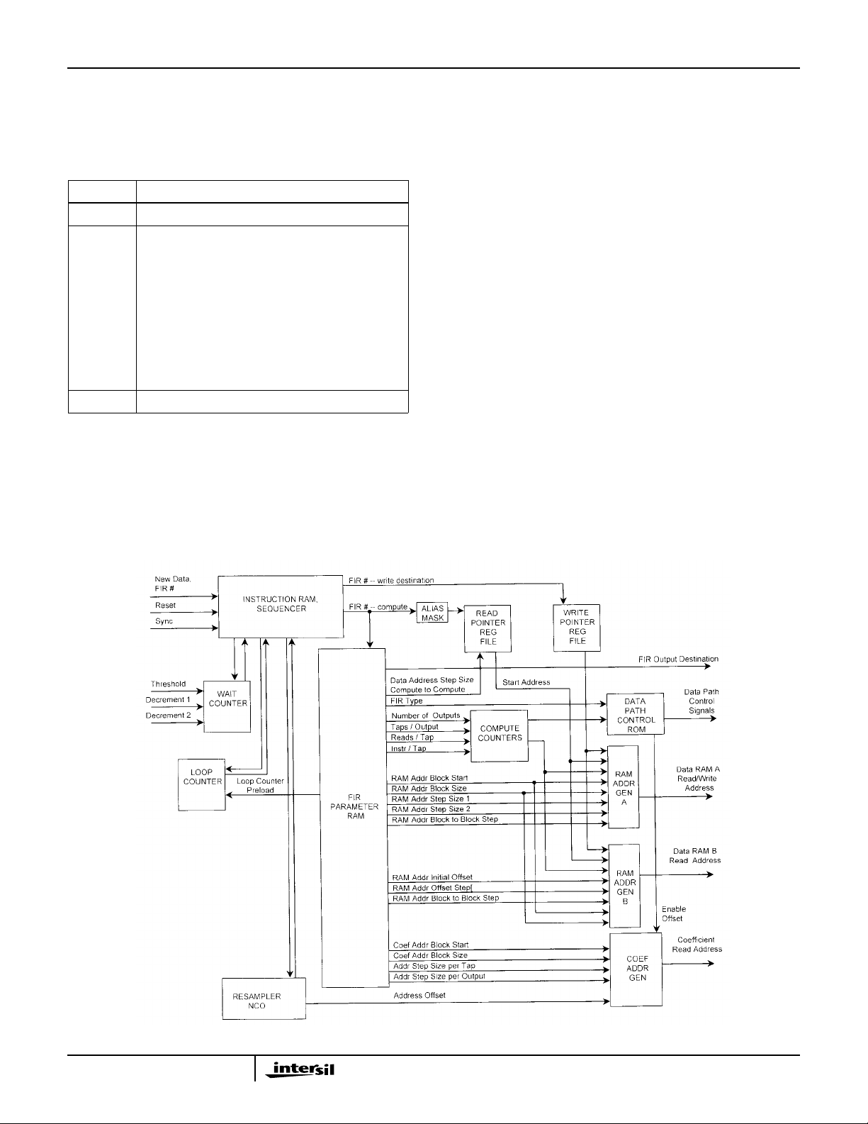
The filter sequencer is programmed via an instruction RAM
and several control registers. These are described below.
Instruction RAMs
The filter compute engine is controlled by a simple
sequencer supporting up to 32 steps. Each step can be a
filter or one of four sequence flow instructions - wait, jump
(conditional or unconditional), load loop counter, or NOP.
There are 128 bits per instruction word with each word
consisting of condition code selects, FIR parameters and
data routing controls. Not all of the instruction word bits are
used for all instruction types. The actual sequencer
instruction is only 9 bits. The rest of the bits are used for filter
parameters or for the loop counter preload. Each sequence
step is loaded in four 32-bit writes. The mapping of the bit
fields for the instruction types is shown in the instruction bit
field table that follows.
When the filter is reset, the instruction pointer is set to 31
(the last instruction step). The read and write pointers are
initialized on reset, so a reset must be done when the
channel is initialized or restarted.
A fixed offset can be added to the starting read address of
the filter in one sequence step. This function is provided to
offset the data reads of the filters in a polyphase filter bank all filters in the bank will write the same data to the same
RAM location. To offset the computations the RAM read
address is offset.
The instruction word bits (127:0) are assigned to memory
words as follows:
• 31:0 to destination C C C C 0 0 0 1 0 x x x x x 0 0
• 63:32 to destination C C C C 0 0 0 1 0 x x x x x 0 1
• 95:64 to destination C C C C 0 0 0 1 0 x x x x x 1 0
• 127:96 to destination C C C C 0 0 0 1 0 x x x x x 1 1
where CCCC is the channel number and xxxxx is the
instruction sequence step number. Note the µPHold bit in
the filter compute engine control register (IWA = *00Ah)
must be set for the microprocessor to read from or write to
the instruction or coefficient RAMs.
14
HSP50216
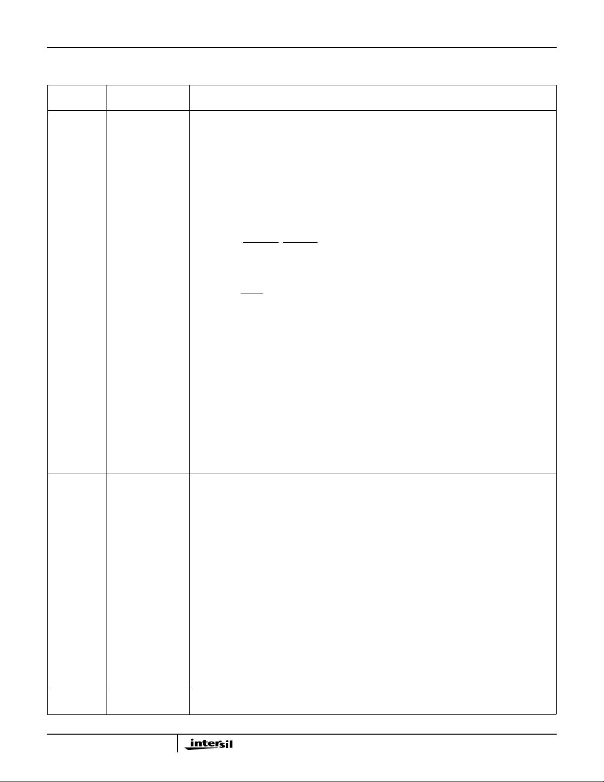
Instruction Bit Fields
INSTRUCTION BIT FIELDS
BIT
POSITIONS FUNCTION DESCRIPTION
8:0 Instruction Instruction Field Bit Mapping
Bit876543210
Type
WAIT00XXXXCCC
FIR 0 1 Start IncrRS DecrSel DecrEn LdLp DecrLp EnU/C
JUMP 1 JJJJJCCC
(NOPs and loading the loop counter are special cases of the FIR instruction)
XXXX = ignored
JJJJJ = jump destination (sequence step number)
CCC = condition code
000 = (waitcount ≥ threshold)
001 = waitcount ≥ threshold
010 = loop counter ≠ 0
011 = loop counter = 0
100 = RSCO Tab (RSCO - resampler NCO carry output)
101 = RSCO
110 = sync (if enabled) or µP controlled bit
111 = always
Start = load parameters and start filter computation, set to zero for no-ops, loop counter loads
IncrRS = increment resampler during this filter.
Increments on start or at each FIR output depending on µPcontrol bit.
DecrSel = selects between two decrement values for the wait counter.
DecrEn = decrement wait count on starting this instruction.
LdLp = load loop counter with the data in the I(20:9) bit field.
The start bit should not be set when this bit is set.
DecrLp = decrement loop counter on starting this instruction.
EnU/C = enable U/C counter with this FIR.
This multiplies the data by 1, j, -1, -j.
The multiplication factor changes each time the filter runs.
14:9 FIR Type FIR Parameter Bit Fields
14:9 FIR type
000000 NOP
000001 Decimating FIR, Even Symmetric, Even # Taps
000010 Decimating FIR, Even Symmetric, Odd # Taps
000011 Decimating FIR, Odd Symmetric, Even # Taps
000100 Decimating FIR, Odd Symmetric, Odd # Taps
000101 Decimating FIR, Asymmetric
001000 Resampling FIR, Asymmetric
001001 Interpolating HBF
100000 Decimating FIR, Complex (Asymmetric)
NOTES:
1. Regular interpolation FIRs are successive runs of a FIR with no data address increment, but with
coefficient start address increments.
2. Decimating HBFs are even symmetric, odd number of taps but with different data step sizes.
3. U/C FIR is a normal FIR with the U/C bit enabled.
4. Other codes may be added in the future.
17:15 Steps per FIR Specifies the number of steps per FIR instruction sequence (load with value minus 1)
(set to 0 for all FIR types except complex which is set to 1)
15

HSP50216
INSTRUCTION BIT FIELDS (Continued)
BIT
POSITIONS FUNCTION DESCRIPTION
28:18 Destination Destination Field Bit Mapping
28 27 26 25 24 23 22 21 20 19 18
AGCLFGN AGCLF Path1 Path0 OS FB F4 F3 F2 F1 F0
AGCLFGNAGC loop gain select. Only applies to Path 1.
Loop gain 0 or 1 if AGCLF bit is set. Set to 0 (1 is a test mode for future chips).
AGCLF AGC loop filter enable. Only applies to Path 1.The AGC loop is updated with the magnitude
of this sample (Path(1:0) = 01).
Path(1:0) Back End Data Routing Path Selection
00 Route output back to filter compute engine input to another FIR in the filter chain.
01 Route output thru the FIFO and AGC forward path to the cartesian-to-polar coordi-
nate converter conversion and output (I1, Q1, magnitude, phase, gain) and also to route to
a discriminator (i.e., dφ/dt FIR).
10 Route output directly to the output, bypassing the FIFO and AGC (I2, Q2). This path
also routes to next channel FIR input.
OS Enable output strobe. Setting this bit generates a data ready signal when the data reaches
the output section and starts the serial output sequence (paths 1, 2, 3). If OS is not set,
there will be no output to the outside world from this channel, for that output calculation, but
the data will be loaded into its output holding register (OS would not be set when routing the
data to another back end when cascading channels).
FB Feedback data path. When set, the magnitude and phase from the cartesian-to-polar coor-
dinate converter block are routed to the filter compute engine input. Provided for discriminator filtering.
F(4:0) Filter select. For data recirculated to the input of the FIR processor by path 0 or from the
cartesian to polar coordinate converter output, these bits tell which filter sequencer step
gets it as an input.
31:29 Round Select 31:29 Round Select (Add rounding bit at specified location)
-24
, use this code when downshifting is not used.
-23
-22
-21
-20
-19
-18
41:32 Data Memory
Block Start
44:42 Data Memory
Block Size
52:45 Data Memory
Block-to-Block Step
000 2
001 2
010 2
011 2
100 2
101 2
110 2
111 no rounding
Provided for use with the coefficient down-shift bits.
Memory block base address, 0-1023, 0-383 are valid for the HSP50216.
44:42 Block Size
08
116
232
364
4 128
5 256
6 512
7 1024
(modulo addressing is used)
0-255, usually equal to the decimation factor for the FIR in this instruction.
16
 Loading...