

®
www.BDTIC.com/Intersil
HSP50214B
Data Sheet May 1, 2007 FN4450.4
Programmable Downconverter
The HSP50214B Programmable Downconverter converts
digitized IF data into filtered baseband data which can be
processed by a standard DSP microprocessor. The
Programmable Downconverter (PDC) performs down
conversion, decimation, narrowband low pass filtering, gain
scaling, resampling, and Cartesian to Polar coordinate
conversion.
The 14-bit sampled IF input is down converted to baseband
by digi
tal mixers and a quadrature NCO, as shown in the
Block Diagram. A decimating (4 to 32) fifth order Cascaded
Integrator-Comb (CIC) filter can be applied to the data
before it is processed by up to 5 decimate-by-2 halfband
filters. The halfband filters are followed by a 255-tap
programmable FIR filter. The output data from the
programmable FIR filter is scaled by a digital AGC before
being re-sampled in a polyphase FIR filter. The output
section can provide seven types of data: Cartesian (I, Q),
polar (R, θ), filtered frequency (dθ/dt), Timing Error (TE), and
AGC level in either parallel or serial format.
Features
• Up to 65MSPS Front-End Processing Rates (CLKIN) and
55MHz Back-End Processing Rates (PROCCLK)
Clocks May Be Asynchronous
• Processing Capable of >100dB SFDR
• Up to 255-Tap Programmable FIR
• Overall Decimation Factor Ranging from 4 to 16384
• Output Samples Rates to ≅ 12.94MSPS with Output
Band
widths to ≅ 982kHz Lowpass
• 32-Bit Programmable NCO for Channel Selection and
Carrier Tracking
• Digital Resampling Filter for Symbol Tracking Loops and
Incommensurate Sample-to-Output Clock Ratios
• Digital AGC with Programmable Limits and Slew Rate to
Opt
imize Output Signal Resolution; Fixed or Auto Gain
Adjust
• Serial, Parallel, and FIFO 16-Bit Output Modes
• Cartesian to Polar Converter and Frequency Discriminator
for AFC Loops and Demodulation of AM, FM, FSK, and
DPSK
• Input Level Detector for External I.F. AGC Support
• Pb-Free Plus Anneal Available (RoHS Compliant)
Applications
• Single Channel Digital Software Radio Receivers
• Base Station Rx’s: AMPS, NA TDMA, GSM, and CDMA
• Compatible with HSP50210 Digital Costas Loop for PSK
Rece
ption
• Evaluation Platform Available
Ordering Information
PART NUMBER PART MARKING TEMP. RANGE (°C) PACKAGE PKG. DWG. NO.
HSP50214BVC HSP50214BVC 0 to +70 120 Ld MQFP Q120.28x28
HSP50214BVCZ (Note) HSP50214BVCZ 0 to +70 120 Ld MQFP (Pb-free) Q120.28x28
HSP50214BVI HSP50214BVI -40 to +85 120 Ld MQFP Q120.28x28
HSP50214BVIZ (Note) HSP50214BVIZ -40 to +85 120 Ld MQFP (Pb-free) Q120.28x28
NOTE: Intersil Pb-free plus anneal products employ special Pbtermination finish, which are RoHS compliant and compatible with both SnPb and Pb-free soldering operations. Intersil Pb-free products are MSL
classified at Pb-free peak reflow temperatures that meet or exceed the Pb-free requirements of IPC/JEDEC J STD-020.
free material sets; molding compounds/die attach materials and 100% matte tin plate
1
Block Diagram
www.BDTIC.com/Intersil
MICROPROCESSOR
C(7:0)
IN(13:0)
GAIN
ADJ
(2:0)
COF
SOF
CLKIN
PROCCLK
REFCLK
READ/WRITE
LEVEL DETECT
INPUT
SECTION
CARRIER
NCO
CONTROL
TH
5
ORDER
CIC
FILTER
TH
5
ORDER
CIC
FILTER
FILTERS
HALFBAND
FILTERS
HALFBAND
HSP50214B
255-TAP
FIR FILTER
255-TAP
FIR FILTER
RESAMPLING
NCO
AGC LOOP FILTER
POLYPHASE
FIR AND
HALFBAND
FILTERS
POLYPHASE
FIR AND
HALFBAND
FILTERS
Δ
I OUT
CARTESIAN
TO
POLAR
COORDINATE
CONVERTER
Q OUT
DISCRIMINATOR
TIMING ERROR
AGC
MAG.
PHASE
FREQ
SEROUTA
SEROUTB
AOUT(15:0)
BOUT(15:0)
OUTPUT FORMATTER
2
FN4450.4
May 1, 2007
Pinout
www.BDTIC.com/Intersil
HSP50214B
HSP50214B
(120 LD MQFP)
TOP VIEW
OEAL
GND
AOUT0
AOUT1
AOUT2
AOUT3
AOUT4
NC
VCCAOUT5
AOUT6
AOUT7
AOUT8
AOUT9
NC
GND
AOUT10
AOUT11
IN11
IN13
IN12
GND
REFCLK
VCCAGCGNSEL
OEAH
AOUT13
AOUT14
AOUT15
AOUT12
IN10
IN9
IN8
GND
IN7
NC
IN6
IN5
IN4
IN3
IN2
GND
IN1
IN0
V
CC
CLKIN
GND
NC
ENI
GAINADJ2
GAINADJ1
GAINADJ0
COF
COFSYNC
GND
SOF
SOFSYNC
V
CC
SYNCIN1
SYNCIN2
103
102
101
100
117
118
119
120
1
2
3
4
5
6
7
8
9
10
11
12
13
14
15
16
17
18
19
20
21
22
23
24
25
26
27
28
29
30
32
31
115
116
333435363738394041424344454647484950515253545556575859
111
112
113
114
105
104
106
107
108
109
110
95
96
97
98
99
91
92
93
94
90
DATARDY
OEBH
89
BOUT15
88
BOUT14
87
V
86
CC
NC
85
BOUT13
84
BOUT12
83
BOUT11
82
BOUT10
81
BOUT9
80
BOUT8
79
GND
78
GND
77
PROCCLK
76
V
75
CC
MSYNCI
74
MSYNCO
73
72
GND
71
BOUT7
70
BOUT6
BOUT5
69
GND
68
BOUT4
67
NC
66
BOUT3
65
BOUT2
64
BOUT1
63
BOUT0
62
OEBL
61
60
3
SYNCOUT
WR
INTRRP
RD
GND
C7
C6NCC5
C3C2C1NCC0A2A1
C4
CC
V
A0
GND
SEL2
SEL1
GND
SEL0
CC
V
SEROE
SEROUTB
SERSYNC
SERCLK
FN4450.4
May 1, 2007
SEROUTA

HSP50214B
www.BDTIC.com/Intersil
Pin Descriptions
NAME TYPE DESCRIPTION
V
CC
GND - Ground.
CLKIN I Input Clock. This clock should be a multiple of the input sample r
IN(13:0) I Input Data. The format of the input data may be set to offset binary or 2’s complement. IN13 is the MSB (see Control
ENI I Input Enable. Active Low. This pin enables the input to the part in one of two modes, gated or interpolated (see
GAINADJ(2:0) I GAINADJ Input. Adds an offset to the gain via the shifter following the mixer. GAINADJ value is added to the shift
PROCCLK I Processing Clock. PROCCLK is the clock for all processing functions fo
AGCGNSEL I AGC Gain Select. This pin selects between two AGC loop gain
COF I Carrier Offset Frequency Input. This serial inpu
COFSYNC I Carrier Offset Frequency Sync. This signal is asserted one CLK befor
SOF I Re-Sampler Offset Frequency Input. This se
SOFSYNC I Re-Sampler Offset Frequency Sync. This signal is asserted
AOUT(15:0) O Parallel Output Bus A. Two parallel output modes are available on th
BOUT(15:0) O Parallel Output Bus B. Two parallel output modes are available on th
- Positive Power Supply Voltage.
ate. All input section processing occurs on the rising
edge of CLKIN. The frequency of CLKIN is designated f
rd 0).
Wo
Control Word 0). In gated mode, one sample is taken per CLKIN when
designated f
co
de from the microprocessor (μP) interface. The shift code is saturated to a maximum code of F . The gain is of fset
by (6dB)(GAINADJ); (000 = 0dB gain adjust; 111 = 42dB gain adjust) GAINADJ2 is the MSB. See “Using the Input
Gain Adjust Control Signals” Section.
performed on PROCCLK’s rising edge. All output timing is derived from this clock.
This clock may be asynchronous to CLKIN.
Gain setting 1 is selected when AGCGNSEL = 1.
(see Serial Interface Section). The offset may be 8, 16, 24, or 32-bit s. The setup and hold times are relative to CLKIN.
This input is compatible with the outp ut o f t he HSP5 0210 Costas loop [1].
frequency word (see Serial Interface Section). The setup and hold times are relative to CLKIN. This input is
compatible with the output of the HSP50210 Costas loop [1].
NCO (see Serial Interface Section). The offset may be 8, 16, 24, or 32-bits. The setup and hold times are relative
to PROCCLK. This input is compatible with the output of the HSP50210 Costas loop [1].
(see Serial Interface Section). The setup and hold times are relative to PROCCLK. This input is compatible with the
output of the HSP50210 Costas loop [1].
Output Port, where the source is selected through Control Word 20 (see the Microprocessor Write Section) and
comes directly from the Output MUX Section (see Output Control Section). The most significant byte of AOUT
always outputs the most significant byte of the Parallel Direct Output Port whose data type is selected via μP
interface. AOUT15 is the MSB. In this mode, the AOUT(15:0) bus is updated as soon as data is available.
is asserted to indicate new data. For this mode, the output choices are: I, |r|, or f. The format is 2’s complement,
except for magnitude, which is unsigned binary with a zero as the MSB.
The second mode for parallel data is called the Buffer RAM Output Port. The Buffer RAM Output Port acts like a
O for blocks of information called data sets. Within a data set is I, Q, magnitude, phase, and frequency
FIF
information; a data type is selected using SEL(2:0). Up to 7 data sets are stored in the Buffer RAM Output Port. The
LSBytes of the AOUT and BOUT busses form the 16-bits for the buffered output mode and can be used for buffered
mode while the MSBytes are outputting data in the direct output mode. For this mode, the output formats are the
same as the Direct Output Port mode.
Output Port, where the source is selected through Control Word 20 (see the Microprocessor Write Section) and
comes directly from the Output MUX Section (see Output Control Section). The most significant byte of BOUT
always outputs the most significant byte of the Parallel Direct Output Port whose data type is selected via μP
interface. BOUT15 is the MSB. In this mode, the BOUT(15:0) bus is updated as soon as data is available.
is asserted to indicate new data. For this mode, the output choices are: Q, φ, or |r|. The format is 2’s complement,
except for magnitude which is unsigned binary with a zero as the MSB.
The second mode for parallel data is called the Buffer RAM Output Port. The Buffer RAM Output Port acts like a
O for blocks of information called data sets. Within a data set is I, Q, magnitude, phase, and frequency
FIF
information; a particular information is selected using SEL(2:0). Up to 7 data sets is stored in the Buffer RAM Output
Port. The least significant byte of BOUT can be used to either output the least significant byte of the B Parallel Direct
Output Port or the least significant byte of the Buffer RAM Output Port. See Output Section. For this mode the output
formats are the same as the Direct Output Port mode.
, which can be different from f
S
when ENI is used.
CLKIN
t pin is used to load the carrier of fset f reque ncy in to t he C arrie r NCO
rial input pin is used to load the offset frequency into the Re-Sampler
.
CLKIN
ENI is asserted. The input sample rate is
llowing the CIC Section. Processing is
s. This input is setup and held relative to PROCCLK.
e the most significant bit (MSB) of the offset
one CLK before the MSB of the offset frequency word
e HSP50214B. The first is called the Direct
e HSP50214B. The first is called the Direct
DATARDY
DATARDY
4
FN4450.4
May 1, 2007

HSP50214B
www.BDTIC.com/Intersil
Pin Descriptions (Continued)
NAME TYPE DESCRIPTION
DATARDY O Output Strobe Signal. Active Low. Indicates when new data from the Direct Output Port Section is available.
OEAH I Output enable for the MSByte of the AOUT bus. Active Low. The AOUT MSByte outputs are three-stated when
OEAL I Output enable for the LSByte of the AOUT bus. Active Low. The AOUT LSByte outputs are three-stated when
OEBH I Output enable for the MSByte of the BOUT bus. Active Low. The BOUT MSByte outputs are three-stated when
OEBL I Output enable for the LSByte of the BOUT bus. Active Low. The BOUT LSByte outputs are three-stated when
SEL(2:0) I Select Address is used to choose which information in a data set fr
INTRRP O Interrupt Output. Active Low. This output is asserted for 8 PROCCLK cycles when the Buffer RAM Output Port is
SEROUTA O Serial Output Bus A Data. I, Q, magnitude, phase, frequ
SEROUTB O Serial Output Bus B Data. Contents may be related to SEROUTA. I, Q, magnitude, phase, frequency, timing error
SERCLK O Output Clock for Serial Data Out. Derived from PROCCLK as give
SERSYNC O Serial Output Sync Signal. Serves as serial da
SEROE I Serial Output Enable. When high, the SEROUTA, SEROUTB, SERCLK, and SERSYNC signals are set to a high
C(7:0) I/O Processor Interface Data Bus. See Microprocessor Write Section. C7 is the MSB.
A(2:0) I Processor Interface Address Bus. See Microprocessor
WR I Processor Interface Write Strobe. C(7:0) is written to Control Words selected by A(2:0) in the Programmable Down
RD I Processor Interface Read Strobe. C(7:0) is read from output or status locations selected by A(2:0) in the
REFCLK I Reference Clock. Used as an input clock for the timing error de
MSYNCO O Multiple Chip Sync Output. Provided for synchronizing multiple parts when CLKIN and PROCCLK are
MSYNCI I Multiple Chip Sync Input. The MSYNCI pin of all the p
SYNCIN1 I CIC Decimation/Carrier NCO Update Sync. Can be used to synchronize the CIC Section, carrier NCO update, or
SYNCIN2 I FIR/Timing NCO Update/AGC Gain Update Sync. Can be used to synchronize the FIR, T
SYNCOUT O S trobe Output. This synchronization signal is generated by the μP
DATARDY is asserted for one PROCCLK cycle during the first clock cycle that data is available on the parallel out
busses. See Output Section.
OEAH is high.
OEAL is high.
OEBH is high.
OEBL is high.
least significant bytes of AOUT and BOUT. SEL2 is the MSB.
ready for reading.
ency, timing error and AGC information can be sequenced
in programmable order. See Output Section and Microprocessor Write Section.
and AGC information can be sequenced in pr
Section.
Section.
impedance.
Converter on the rising edge of this signal. See Microprocessor Write Section.
Programmable Down Converter on the falling edge of this signal. See Microprocessor Read Section.
REFCLK. REFCLK frequency must be less than or equal to PROCCLK/2.
asynchro
back end processing operating under PROCCLK. This output sync signal from one part is connected to the MSYNCI
signal of all the HSP50214Bs.
NOTE: MSYNCI must be connected t
both. See
High.
gain update, or any combination of the above. See the Multiple Chip Synchronization Section and Control Words 7,
8, and 10 in the Microprocessor Write Section. Active High.
generated by PROCLK or CLKIN (see Control Word 0 and Control Word 24 in the Microprocessor Write Section).
Active High.
nous. MSYNCO is the synchronization signal between the input section operating under CLKIN and the
the Multiple Chip Synchronization Section and Control Word 0 in the Microprocessor Write Section. Active
ogrammable order. See Output Section and Microprocessor Write
ta strobes. See Output Section and Microprocessor Write Section.
Write Section. A2 is the MSB.
arts should be tied to the MSYNCO of one part.
o an MSYNCO signal for operation.
om the Buffer RAM Output Port is sent to the
n by Control Word 20 in the Microprocessor Write
tector. The timing error is computed relative to
iming NCO update, AGC
interface for synchronizing multiple parts. Can be
5
FN4450.4
May 1, 2007
6
www.BDTIC.com/Intersil
AGCGNSEL
PROCCLK
GAINADJ(2:0)
ENI
IN(13:0)
DETECT
μPROCESSOR
INTERFACE
CLKIN
INPUT
LEVEL
TO
SECTION
MIXER
5TH ORDER
CIC
DECIMATE
FROM 4-32
TO OUTPUT FORMATTER
AND MICROPROCESSOR
0 TO 5 HALFBAND FILTER;
DECIMATION UP TO 32
INTERFACE
(CO = 1;
= 0)
C
n
255-TAP
PROGRAMMABLE
FIR FILTER
(DECIMATE UP TO 16)
AGCOUT
SHIFT
AGC
A
LIMIT
FILTER
POLYPHASE
RE-SAMPLER
LOOP
FILTER
INTERPOLATE
BY 2/4
HALFBAND
FILTERS
ERROR
DETECT
CARTESIAN
TO
POLAR
I
I2Q2+
Q
⎛⎞
----
atan
⎝⎠
I
Q
DATARDY
INTRRP
AOUT(15:0)
BOUT(15:0)
OEAH
OEAL
OEBH
OEBL
HSP50214B
(C
COS
COF
COFSYNC
(CARRIER TRACKING)
SOF
SOFSYNC
REFCLK
RD
WR
A(2:0)
C(7:0)
May 1, 2007
FN4450.4
SIN
NCO
MICROPROCESSOR
READ/WRITE
CONTROL
SECTION
OUTPUT SECTION
DISCRIMINATOR SECTION
INPUT SECTION
LEVEL DETECT SECTION
SYNCHRONIZATION SECTION
CARRIER NCO SECTIONS
CIC, HALFBAND FILTER, AND FIR SECTIONS
DIGITAL AGC SECTION
RE-SAMPLER/INTERPOLATION HALFBAND SECTION
TIMING NCO
= 1;
O
= 0)
C
n
(SYMBOL TRACKING)
SHIFT
NCO
FILTER
POLYPHASE
DIFFERENCE
CLKIN
PROCCLK
DISCRIMINATOR
dθ
PROGRAMMABLE
td
63-TAP
FIR FILTER
TIMING ERROR
AGCOUT
A
CHIP
SYNCHRONIZATION
CIRCUITRY
BACK END
SYNCHRONIZATION
CIRCUITRY
FRONT END
SYNCHRONIZATION
CIRCUITRY
OUTPUT FORMATTER
INTRRP
SEL(2:0)
SEROUTA
SEROUTB
SERCLK
SERSYNC
SEROE
MSYNCI
SYNCOUT
MSYNCO
SYNCIN2
SYNCIN1
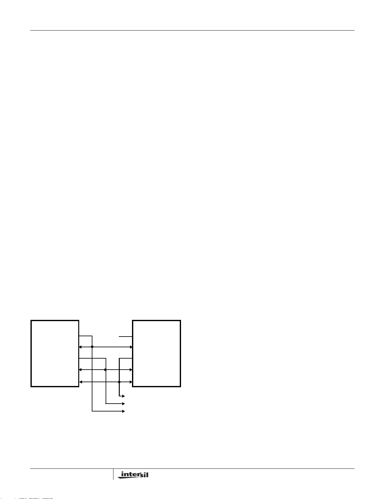
FIGURE 1. FUNCTIONAL BLOCK DIAGRAM OF THE HSP50214B PROGRAMMABLE DOWNCONVERTER

HSP50214B
www.BDTIC.com/Intersil
Functional Description
The HSP50214B Programmable Downconverter (PDC) is an
agile digital tuner designed to meet the requirements of a
wide variety of communications industry standards. The
PDC contains the processing functions needed to convert
sampled IF signals to baseband digital samples. These
functions include LO generation/mixing, decimation filtering,
programmable FIR shaping/bandlimiting filtering,
resampling, Automatic Gain Control (AGC), frequency
discrimination and detection as well as multi-chip
synchronization. The HSP50214B interfaces directly with a
DSP microprocessor to pass baseband and status data.
A top level functional block diagram of the HSP50214B is
sh
own in Figure 1. The diagram shows the major blocks and
multiplexers used to reconfigure th
e data path for various
architectures. The HSP50214B can be broken into 13
sections: Synchronization, Input, Input Level Detector,
Carrier Mixer/Numerically Control Oscillator (NCO), CIC
Decimating Filter, Halfband Decimating Filter, 255-Tap
Programmable FIR Filter, Automatic Gain Control (AGC),
Re-sampler/Halfband Filter, Timing NCO, Cartesian to Polar
Converter, Discriminator, and Output Sections. All of these
sections are configured through a microprocessor interface.
The HSP50214B has three clock inputs; two are required and
on
e is optional. The input level detector , carrier NCO, and CIC
decimating filter sections operate on the rising edge of the
input clock, CLKIN. The halfband filter , p rogrammable FIR
filter, AGC, Re-Sampler / Halfband filters, timing NCO,
di
scriminator, and ou tput sections ope ra te on the ri si ng edge
of PROCCLK. The third clock, REFCLK, is used to generate
timing error information.
NOTE: All of the clocks may be asynchronous.
PDC Applications Overview
This section highlights the motivation behind the key
programmable features from a communications system level
perspective. These motivations will be defined in terms of ability
to provide DSP processing capability for specific modulation
formats and communication applications. The versatility of the
Programmable Downconverter can be intimidating because of
the many Control Words required for chip configuration. This
section provides system level insight to help allay reservations
about this versatile DSP product. It should help the designer
capitalize on the greatest feature of the PDC - VERSATILITY
THROUGH PROGRAMMABILITY. It is this feature, when fully
understood, that brings the greatest return on design
investment by offering a single receiver design that can process
the many waveforms required in the communications
marketplace.
FDM Based Standards and Applications
Table 1 provides an overview of some common frequency
division multiplex (FDM) base station applications to which the
PDC can be
applied. The PDC provides excellent selectivity
for frequency division multiple access (FDMA) signals. This
high selectivity is achieved with 0.012Hz resolution frequency
control of the NCO and the sharp filter responses capable with
a 255-tap, 22-bit coefficient FIR filter . The 16-bi t resolution out
of the Cartesian to Polar Coordinate Converter are routed to
the frequency detector, which is follow ed by a 63-t ap, 22-bit
coefficient FIR filter structure for facilitating FM and FSK
detection. The 14-bit input resolution is the smallest bit
resolution found throughout the conversion and filtering
sections, providing excellent dynamic range in the DSP
processing. A unique input gain scaler adds an additional
42dB of range to the input level variation, to compensate for
changes in the analog RF front end receive equipment.
Synchronization circuitry allows precise timing control of the
base station reconfiguration for all receive channels
simultaneously. Portions of this table were corroborated with
reference [2].
TABLE 1. CELLULAR PHONE BASE STA TION
STANDARD
RX BAND
CHANNEL
BW (kHz)
# TRAFFIC
CHANNELS
MODULA-
DEVIATION
CONTROL
MOD
DEVIATION
CONTROL
HANNEL
C
APPLICATIONS USING FDMA
(MHz)
VOICE
TION
PEAK
(kHz)
ULATION
PEAK
(kHz)
RATE
(Kbps)
AMPS
(
IS-91)
824-849 925-940 453-458
832 600
FSK FSK FSK FSK FSK
MCS-L1
MCS-L2
30 25.0
12.5
1200
FM FM FM FM FM
12 5 5 4 9.5
8 4.5 3.5 2.5 6.4
10 0.3 1.2 5.3 8
NMT-400
NMT-900 C450
890-915
12.5
200
1999
451-456 871-904
25
20.0
10.0
222
444
ETACS
NTACS
915-925
25.0
12.5
1240
800
TDM Based Standards and Applications
Table 2 provides an overview of some common Time D ivision
Multiplexed (TDM) base station applications to which the PDC
can be ap
applications, such as North American TDMA (IS136), where
30kHz is the received band of interest for the PCS
basestation, the PDC offers 0.012Hz frequency resolution in
downconversion in addition to α = 0.35 matched
(programmable) filtering capability. The π/4 DPSK modulation
can be processed using the PDC Cartesian to Polar
coordinate converter and dφ/dt detecto r circuitry or by
processing the I/Q samples in the DSP μP. The PDC provides
plied. For time division multiple access (TDMA)
7
FN4450.4
May 1, 2007
HSP50214B
www.BDTIC.com/Intersil
the ability to change the received signal gain and frequency,
synchronous with burst timing. The synchronous gain
adjustment allows the user to measure the power of the signal
at the A/D at the end of a burst, and synchronously reload that
same gain value at the arrival of the next user burst.
For applications other than cellular phones (where the
prea
mbles are not changed), the PDC frequency
discriminator output can be used to obtain correlation on the
preamble pattern to aid in burst acquisition.
TABLE 2. CELLULAR BASESTATION APPLICATIONS USING
CHANNEL BW (kHz) 200 200 30
# TRAFFIC CHANNELS 8 16 3
VOICE MODULATION GMSK GMSK
CHANNEL RATE (Kbps) 270.8 270.8 48.6
CHANNEL RATE (Kbps) 270.8 270.8 48.6
Several applications are combinations of frequency and time
domai
TDMA signal that is frequency hopped. The individual
channels contain Gaussian MSK modulated signals. The
PDC again offers the 0.012Hz tuning resolution for dehopping the received signal. The combination of halfband
and 256-tap programmable, 22-bit coefficient FIR filters
readily performs the necessary matched filtering for
demodulation and optimum detection of the GMSK signals.
TDMA
STANDARD GSM PCN IS-54
TYPE Cellular Cellular Cellular
BASESTATION RX
BAN
D (MHz)
CONTROL
MODULATION
n multiple access schemes. For example, GSM is a
935-960 1805-1880 824-849
π/4
DQPSK
GMSK GMSK
π/4
DQPSK
CDMA Based Standards and Applications
For Code Division Multiple Access (CDMA) type signals, the
PDC offers the ability to have a single wideband RF front
end, from which it can select a single spread channel of
interest. The synchronization circuitry provides for easy
control of multiple PDC for applications where multiple
received signals are required, such as base-stations.
In IS-95 CDMA, the receive signal bandwidth is
app
roximately 1.2288MHz wide with many spread spectrum
channel in the band. The PDC supplies the downconversion
and filtering required to receive a single RF channel in the
presence of strong adjacent interference. Multiple PDC’s
would be sourced from a single receive RF chain, each
processing a different receive frequency channel. The
despreader would usually follow the PDC. In some very
specific applications, with short, fixed codes, the filtering and
despreading may be possible with innovative use of the
programmable, 22-bit coefficient FIR filter. The PDC offers
0.012Hz resolution on tuning to the desired receive channel
and excellent rejection of the portions of the band not being
processed, via the halfband and 255-tap programmable, 22bit coefficient FIR filter.
Traditional Modulation Formats
AM, ASK, FM AND FSK
The PDC has the capability to fully demodulate AM and FM
lated waveforms. The PDC outputs 15-bits of amplitude
modu
or 16-bits of frequency for these modulation formats. The FM
discriminator has a 63-tap programmable, 22-bit coefficient FIR
filter for additional signal conditioning of the FM signal. Digital
versions of these formats, ASK and FSK are also readily
processed using the PDC. Just as in the AM modulated case,
ASK signals will use 15-bit magnitude output of the Cartesian to
Polar Coordinate converter. Multi-tone FSK can be processed
several ways. The frequency information out of the
discriminator can be used to identify the received tone, or the
filter can be used to identify and power detect a specific tone of
the received signal. AMPS is an example of an FM application.
PM AND PSK
The PDC provides the downcon
matched filtering and coordinate conversion required for
demodulation of PM and PSK modulated waveforms. These
modulation formats will require external carrier and symbol
timing recovery loop filters to complete the receiver design.
The PDC was designed to interface with the HSP50210
Digital Costas Loop to implement the carrier phase and
symbol timing recovery loop filters (for continuous PSK
signals-not burst).
Digital modulation formats that combine amplitude and
ph
ase for symbol mapping, such as m-ary QAM, can also be
downconverted, demodulated, and matched filtered. The
received symbol information is provided with 16-bits of
resolution in either Cartesian or Polar coordinates to
facilitate remapping into bits and to recover the carrier
phase. External Symbol mapping and Carrier Recovery
Loop Filtering is required for this waveform.
version, demodulation,
Resampling and Interpolation Filters
Two key features of the resampling FIR filter are that the resampler filter allows the output sample rate to be
programmed with millihertz resolution and that the output
sample rate can be phase locked to an independent
separate clock. The re-sampler frees the front end sampling
clocks from having to be synchronous or integrally related in
rate to the baseband output. The asynchronous relationship
between front end and back end clocks is critical in
applications where ISDN interfaces drive the baseband
interfaces, but the channel sample rates are not related in
any way. The interpolation halfband filters can increase the
rate of the output when narrow frequency bands are being
processed. The increase in output rate allows maximum use
of the programmable FIR while preserving time resolution in
the baseband data.
8
FN4450.4
May 1, 2007
HSP50214B
www.BDTIC.com/Intersil
14-Bit Input and Processing Resolution
The PDC maintains a minimum of 14-bits of processing
resolution through to the output, providing over 84dB of
dynamic range. The 18-bits of resolution on the internal
references provide a spurious floor that is better than 98dBc.
Furthermore, the PDC provides up to 42dB of gain scaling to
compensate for any change in gain in the RF front end as
well as up to 96dB of gain in the internal PDC AGC. This
gain maximizes the output resolution for small signals and
compensates for changes in the RF front end gain, to handle
changes in the incoming signal.
Summary
The greatest feature of the PDC is its ability to be
reconfigured to process many common standards in the
communications industry. Thus, a single hardware element
can receive and process a wide variety of signals from PCS
to traditional cellular, from wireless local loop to SATCOM.
The high resolution frequency tuning and narrowband
filtering are instrumental in almost all of the applications.
Multiple Chip Synchronization
Multiple PDCs are synchronized using a MASTER/SLAVE
configuration. One part is responsible for synchronizing the
front end internal circuitry using CLKIN while another part is
responsible for synchronizing the backend internal circuitry
using PROCCLK.
The PDC is synchronized with other PDCs using
lines: SYNCOUT, SYNCIN1, SYNCIN2, MSYNCO, and
MSYNCI. Figure 2 shows the interconnection of these five
signals for multiple chip synchronization where different
sources are used
PDC A is the Master sync through MSO.
PDC B configures the CLKIN sync through SYNCIN1.
PDC A configures the PROCCLK sync through SYNCIN2.
HSP50214B
(MASTER
SYNCIN2)
for CLKIN and PROCCLK.
AB
MSYNCO
MSYNCI
SYNCOUT
SYNCIN2
SYNCIN1
ALL OTHER SYNCIN1
ALL OTHER SYNCIN2
ALL OTHER MSI
FIGURE 2. SYNCHRONIZATION CIRCUIT
SYNCOUT for PDC B should be set to be synchronous with
C
LKIN (Control Word 0, Bit 3 = 0. See the Microprocessor
Write Section). SYNCOUT for PDC B is tied to the SYNCIN1
of all the PDCs. The SYNCIN1 can be programmed so that
five control
HSP50214B
MSYNCO
MSYNCI
SYNCOUT
SYNCIN2
SYNCIN1
(MASTER
SYNCIN1)
the carrier NCO and/or the 5th order CIC filter of all PDCs can
be synchronously loaded / updated using SYNCIN1. See
Co
ntrol Word 0, Bits 19 and 20 in the Microprocessor W ri te
Section for details.
SYNCOUT for one of the PDC’s other than PDC B, should
be
set for PROCCLK (bit 3 = 1 in Control Word 0). This
output signal is tied to the SYNCIN2 of all PDCs. The
SYNCIN2 can be programmed so that the AGC updates its
accumulator with the content s in the master registers
(Control Word 8, Bit 29 in the Microprocessor Write Section).
SYNCIN2 is also used to load or reset the timing NCO using
bit 5, Control Word 11. The halfband and FIR filters can be
reset on SYNCIN2 using Control Word 7, Bit 21. The
MSYNCO of one of the PDCs is then used to drive the
MSYNCI of all the PDCs (including its own).
For application configuration
s where CLKIN and PROCCLK
have the same source, SYNCIN1 and SYNCIN2 can be tied
together. However, if different enabling is desired for the
front end and backend processing of the PDC’s, these
signals can still be controlled independently.
In the HSP50214B, the Control Word 25 reset signal has
be
en extended so that the front end reset is 10 CLKIN
periods wide and the back end reset is 10 PROCCLK
periods wide. This guarantees that no enables will be caught
in the pipelines. In addition, the SYNCIN1 internal reset
signal, which is enabled by setting Control Word 7,
Bit 21 = 1, has been extended to 10 cycles.
In summary, SYNCIN1 is used to update carrier phase
of
fset, update carrier center frequency, reset CIC decimation
counters and reset the carrier NCO (clear the feedback in
the NCO). SYNCIN2 is used to reset the HB filter, FIR filter,
re-sampler / HB state machines and the output FIFO, load a
ne
w gain into the AGC and load a new re-sampler NCO
center frequency and phase offset.
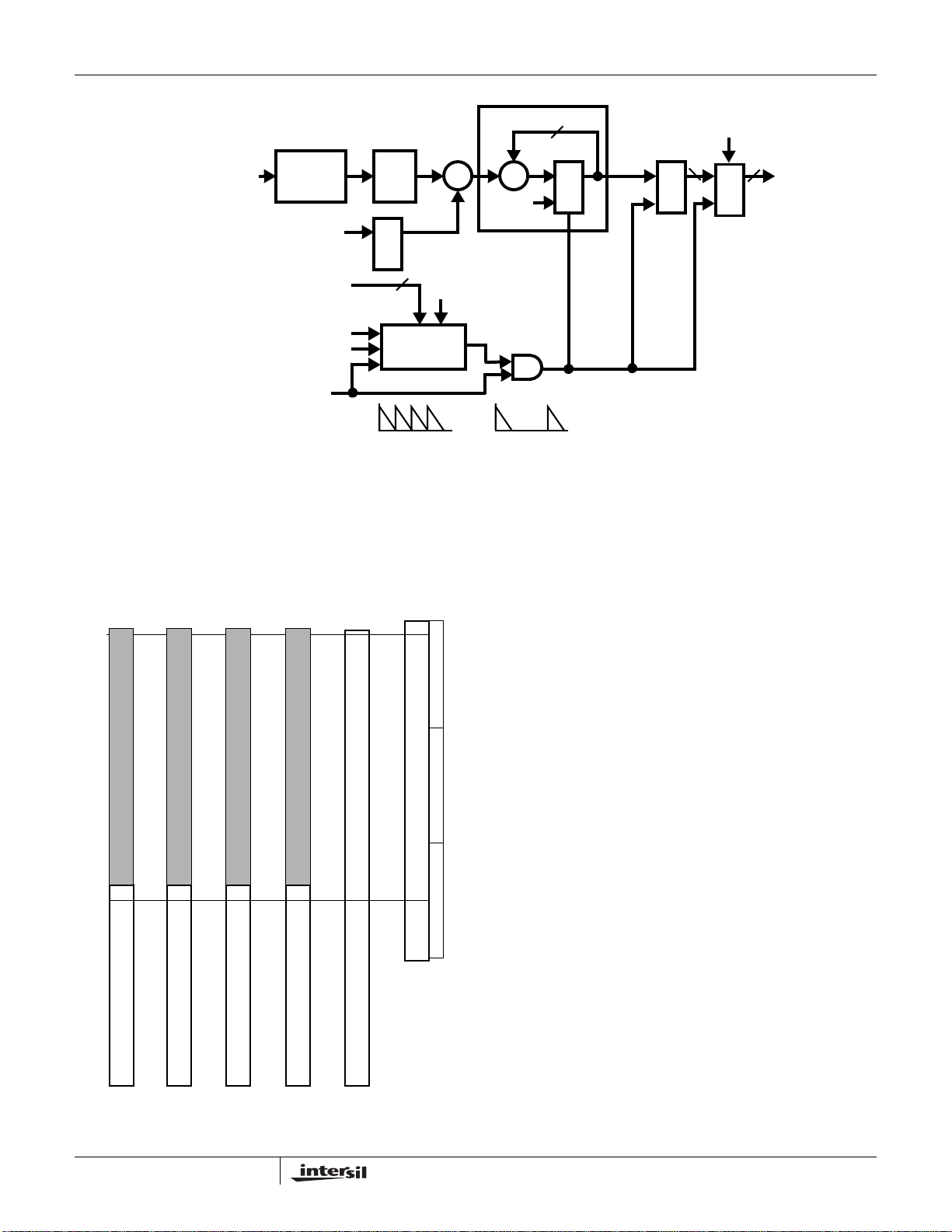
Input Section
The block diagram of the input controller is provided in
Figure 3. The input can support offset binary or two’s
complement data and can be o
interpolated mode (see Control Word 0 from the
Microprocessor Write Section). The gated mode takes one
sample per clock when the input enable (ENI) is asserted.
The gated mode allows the user to synchronize a low speed
sampling clock to a high speed CLKIN.
The interpolated mode allows the user
sample rate and to zero-stuff the data prior to filtering. This
zero stuffing effectively interpolates the input signal up to the
rate of the input clock (CLKIN). This interpolated mode
allows the part to be used at rates where the sampling
frequency is above the maximum input rate range of the
halfband filter section, and where the desired output
bandwidth is too wide to use a Cascaded Integrator Comb
(CIC) filter without significantly reducing the dynamic range.
perated in gated or
to input data at a low
9
FN4450.4
May 1, 2007
HSP50214B
www.BDTIC.com/Intersil
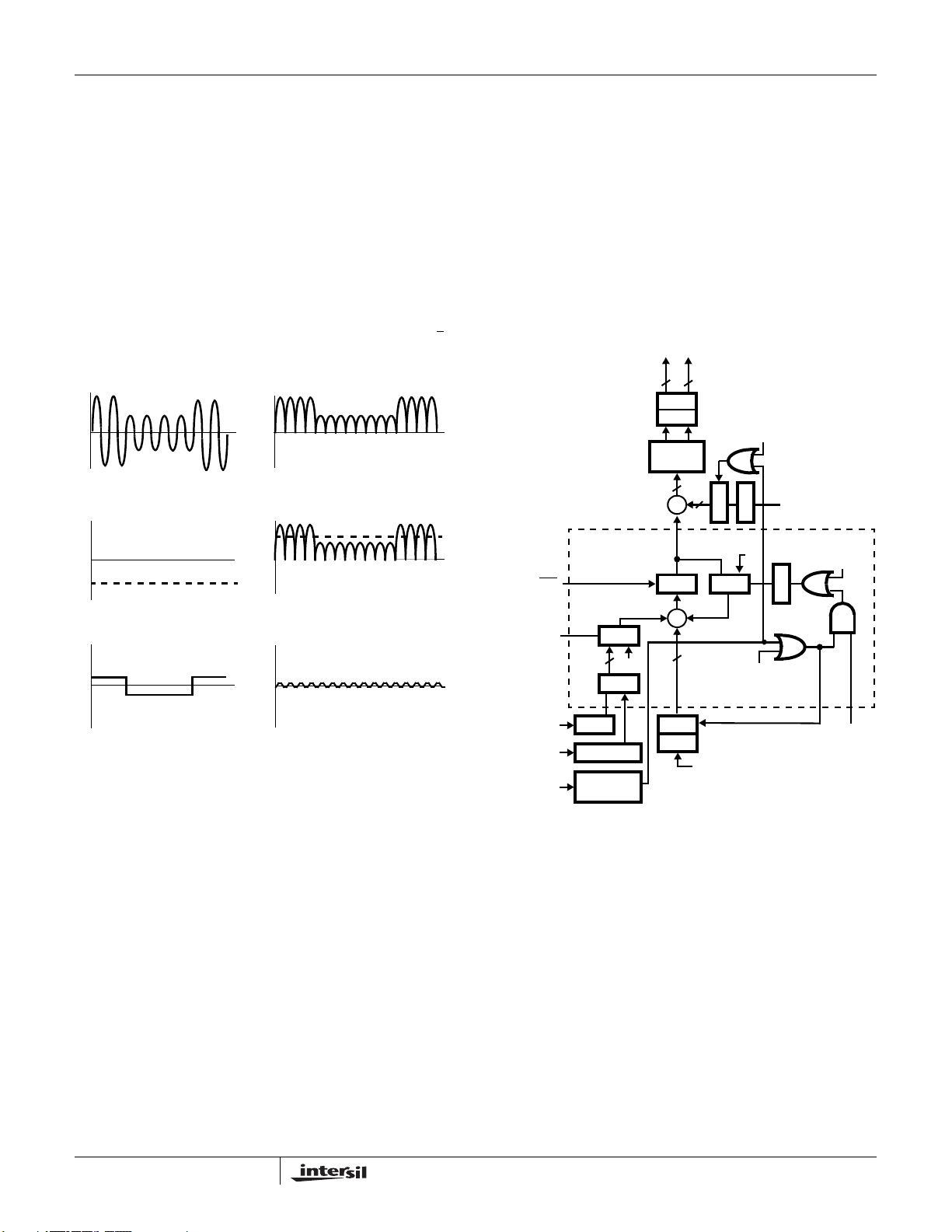
See Figures 4 to 7 for an interpolated input example,
detailing the associated spectral results.
Interpolation Example:
The specifications for the interpolated input example are:
CLKIN = 40MHz
Input Sample Rate = 5MSPS
PROCCLK = 28MHz
Interpolate by 8, Decimate by 10
Desired 85dB dynamic range output bandwidth = 500kHz
Input Level Detector
The Input Level Detector Section measures the average
magnitude error at the PDC input for the microprocessor by
comparing the input level against a programmable
threshold and then integrating the result. It is intended to
provide a gain error for use in an AGC loop with either the
RF/IF or A/D converter stages (see Figure 8). The AGC
loop includes Input Level Detector
an external gain control amplifier (or attenuator). The input
samples are rectified and added to a threshold
IN(13:0)
INPUT FORMAT
INPUT
FORMAT
†
GAINADJ(2:0)
, the microprocessor and
LEVEL
DETECT
REG
REG
INPUT LEVEL DETECTOR †
STATUS (0)
14
14
18
NCO††
EN
programmed via the microprocessor interface, as shown in
Figure 9. The bit weighting of the data path through the
input threshold detector is shown in Figure 10. The
threshold is a signed number, so it should be set to the
inverse of the de
to zero if the average input level is desired instead of the
error. The sum of the threshold and the absolute value of
the input is accumulated in a 32-bit accumulator. The
accumulator can handle up to 2
overflow. The integration time is controlled by an 18-bit
counter. The integration counter preload (ICPrel) is
programmed via the microprocessor interface through
Control Word 1. Only the upper 16-bits are programmable.
The 2 LSBs are always zero. Control Word 1, Bits 29-14
are programmed to:
ICPrel N()41+⁄=
where N is the desired integration period, defined as the
nu
mber of input samples to be integrated. N must be a
multiple of 4: [0, 4, 8, 12, 16 .... , 2
†
INPUT_THRESH †
INTG_MODE †
INTG_INTEVAL
15
REGREG
15
18
LIMIT
DELA Y 3
3
sired input level. The threshold can be set
18
samples without
(EQ. 1)
18
].
†
MUX
SHIFT
4
BYPASS †
CIC
∑
ENI
INTERP †
CONTROL WORD 0
CONTROL WORD 1
CLKIN
BYPASS
5MHz
CLKIN = 5MHz
Without Interpolation, the CIC bypass path exceeds the HB/FIR filter
inp
ut sample rate and the CIC filter path will not yield the desired
85dB dynamic range band width of 500kHz.
CIC
FILTER
MIN. R = 4
FIGURE 4. STATEMENT OF THE PROBLEM
PROCCLK = 28MHz
HB/FIR FILTER
MUX
MAX. fS = 4MHz
(EXCEEDED IN
BYPASS PATH)
CONTROL
LOGIC
FIGURE 3. BLOCK DIAGRAM OF THE INPUT SECTION
500kHz = 85dB
BANDWIDTH
(NOT ACHIEVED
WITH CIC FILTER
PATH)
INPUT_MODE †
INPUT_FMT †
INPUT_THRESH†
INTG_MODE†
INTG_INTEVAL†
DELA Y 3
4
†† See NCO Section for more details.
↑8 (0 STUFF) = 40MHz
5MHz
CLKIN = 40MHz
FIGURE 5. BLOCK DIAGRAM OF THE INTERPOLATION
CIC FILTER
10
† Controlled via microprocessor interface.
4MHz
R = ↓10
APPROACH
HB/FIR FILTER
500kHz = 85dB
BANDWIDTH
FN4450.4
May 1, 2007
HSP50214B
www.BDTIC.com/Intersil
f
S
5MHz 10MHz 15MHz 20MHz 25MHz 30MHz 35MHz 40MHz 45MHz 50MHz
5MHz 10MHz 15MHz 20MHz 25MHz 30MHz 35MHz 40MHz
2f
3f
S
THE INPUT DATA SPECTRUM SAMPLED AT RATE R = f
4f
S
5f
S
S
6f
S
7f
8f
S
S
f’S f’S/2 f’S/4 f’S/8 3f’S/8 5f’S/8 7f’S/8 3f’S/4
9f
S
10f
S
S
FIGURE 6. INTERPOLATION SPECTRUM: INTERPOLATE BY 8 THE INPUT DATA WITH ZERO STUFFING; SAMPLE AT RATE R = f’s
8MHz 12MHz 16MHz 20MHz 24MHz 28MHz 32MHz 36MHz 40MHz
4MHz
DECIMATE BY 10 AND CIC FILTER; SAMPLE AT RATE R = f’s/10
85dB DYNAMIC RANGE BANDWIDTH
4MHz2MHz1MHz 3MHz
CIC FILTER
FREQUENCY
RESPONSE
CIC FILTER ALIAS PROFILE
O.5MHz
FIGURE 7. ALIAS PROFILE AND THE 85dB DYNAMIC RANGE BANDWIDTH
INPUT
μPROC
DAC
IF
GCA
A/D
INPUT LEVEL
DETECTOR (24-BIT
ERROR VALUE)
THRESH
PDC
FIGURE 8. PROCESSOR BASED EXTERNAL IF AGC
11
FN4450.4
May 1, 2007
HSP50214B
www.BDTIC.com/Intersil
INPUT
|X|
R
E
G
16
COUNTER
CONTINUOUS SINGLE
ACCUMULATOR
18
2
17
2
16
2
15
2
14
2
13
2
12
2
11
2
10
2
9
2
8
2
7
2
6
2
5
2
4
2
3
2
2
2
1
2
0
2
-1
2
-2
2
-3
2
-4
2
-5
2
-6
2
-7
2
-8
2
-9
2
-10
2
-11
2
-12
2
-13
2
μPROC READ
0
18
2
17
2
16
2
15
2
14
2
13
2
12
2
11
2
10
2
9
2
8
2
7
2
6
2
5
2
4
2
3
2
2
2
1
2
0
2
-1
2
-2
2
-3
2
-4
2
-6dB
-12dB
-18dB
-24dB
-30dB
-36dB
-42dB
-48dB
-54dB
-60dB
-66dB
-72dB
-78dB
IN(13:0)
INPUT_THRESHOLD †
INTEGRATION_INTERVAL†
INTEGRATION_MODE †
† Controlled via microprocessor interface.
A/D
OUTPUT
f
0
2
S
-1
2
-2
2
-3
2
-4
2
-5
2
-6
2
-7
2
-8
2
-9
2
-10
2
-11
2
-12
2
-13
2
INPUT
0
2
-1
2
-2
2
-3
2
-4
2
-5
2
-6
2
-7
2
-8
2
-9
2
-10
2
-11
2
-12
2
-13
2
0
2
2
2
2
2
2
2
2
2
2
2
2
2
MAGNITUDE
-1
-2
-3
-4
-5
-6
-7
-8
-9
-10
-11
-12
-13
GATING
LOGIC
START †
CLKIN
THESHOLD
0
-2
-1
2
-2
2
-3
2
-4
2
-5
2
-6
2
-7
2
-8
2
-9
2
-10
2
-11
2
-12
2
-13
2
FIGURE 10. INPUT THRESHOLD DETECTOR BIT WEIGHTING
+ +
“0”
FIGURE 9.
READ CODE A(2:0)
PORTS
000 010001
ACCUMULATOR
32
CLKIN
R
E
G
R
E
G
ADDR(2:0)
24
M
U
X
TO
μPROC
8
The integration period counter can be set up to run
continuously or to count down and stop. Continuous integration
counter operation lets the counter run, with sampling occurring
every time the counter reaches zero. Because the processor
samples the detector read port asynchronous to the CLKIN,
data can be missed unless the status bit is monitored by the
processor to ensure that a sample is taken for every integration
count down sequence.
Additionally , in the HSP50214B, the ability to alig n the
st
art/restart of the input level detector integration period with
an external event is provided. This allows the sync signals,
which are synchronized to external events, to be used to align
all of the gain adjustments or measurements. If Control W ord
27, Bit 17 is set to a logic one, the SYNCIN1 signal will cau se
the input level detector to start/restart its integration peri od. If
Control Word 27, Bit 17 is set to a logic zero, control of the
start/restart of the input level detector integration period does
not respond to SYNCIN1.
In the count down and stop mode, the microprocessor read
command
s can be synchronized to system events, such as the
start of a burst for a TDMA application. The integration counter
can be started at any time by writing to Control Word 2. At the
end of the integration period (counter = 0000), the upper 23-bits
of the accumulator are transferred to a holding register for
reading by the microprocessor. Note that it is not the restarting
of the counter (by writing to Control Word 2) that latches the
current value, but the end of the integration count. When the
accumulator results are latched, a bit is set in the Status
Register to notify the processor. Reading the most significant
byte of the 23-bits clears the status bit. See the Microprocessor
Read Section. Figure 11 illustrates a typical AGC detection
process.
12
FN4450.4
May 1, 2007
HSP50214B
www.BDTIC.com/Intersil
Typically, the average input error is read from the Input Level
Detector port for use in AGC Applications. By setting the
threshold to 0, however, the average value of the input signal
can be read directly. The calculation is:
dBFS
RMS
20() 1.111()level()N()16()()⁄[]log=
(EQ. 2)
where “level” is the 24-bit value read from the 3 level
Detector Registers and
“N” is the number of samples to be
integrated. Note that to get the RMS value of a sinusoid,
multiply the average value of the rectified sinusoid by 1.111.
For a full scale input sinusoid, this yields an RMS value of
approximately 3dBf
NOTE: 1.111 scales the rectified sinusoid average (2/π) to 1/ √2
.
A) INPUT SIGNAL
AMPLITUDE
C) THRESHOLD
AMPLITUDE
E) DETECTOR OUTPUT
AMPLITUDE
FIGURE 11. SIGNAL PROCESSING WITHIN LEVEL DETECTOR
.
S
B) RECTIFIED SIGNAL
AMPLITUDEAMPLITUDE
D) ACCUMULATOR INPUTS
F) CLOSED LOOP STEADY STATE
(CONSTANT INPUT)
AMPLITUDE
In the HSP50214B, the polarity of the LSB’s of the
integration period pre-load is selectable. If Control Word 27,
Bit 23 is set to a logic one, the two LSB’s of the integration
period preload are set to logic ones. This allows a power of
two to be set for the integration period, for easy
normalization in the processor. If Control Word 27, Bit 23 is
set to a logic zero, then the two LSB’s of the integration
period preload are set to zeros as in the HSP50214.
Carrier Synthesizer/Mixer
The Carrier Synthesizer/Mixer Section of the HSP50214B is
shown in Figure 12. The NCO has a 32-bit phase
accumulator, a 10-bit phase offset adder, and a sine/cosine
ROM.
The frequency of the NCO is the sum of a center
frequency Control Word, loaded via the microprocessor
interface (Control Word 3, Bits 0 to 31), and an offset
frequency, loaded serially via the COF and COFSYNC pins.
The offset frequency can be zeroed in Control Word 0, Bit 1.
Both frequency control terms are 32-bits and the addition is
modulo 2
32
. The output frequency of the NCO is computed
as:
fCfS* N 232()⁄ ,=
(EQ. 3)
or in terms of the programmed value:
NINTf
C
232fS⁄×[]
HEX
, =
where N is the 32-bit sum of the
terms, f
is the frequency of the carrier NCO sinusoids, fS is
C
center and offset frequency
(EQ. 3A)
the input sampling frequency, and INT is the integer of the
computation. See the Microprocessor Write Section on
instructions for writing Control Word 3.
TO MIXERS
PHASE
ACCUMULATOR
ENI
18 18
REG
REG
SIN/COS
ROM
18
+
REG
SINCOS
CARRIER
PHASE
STROBE
†
R
R
10
E
G
MUX
CARRIER
E
PHASE
G
OFFSET
†
CLEAR
0
R
E
G
PHASE
ACCUM
†
+
COF
ENABLE†
COFSYNC
COF
SYNCIN1
MUX
32
COF
REG
SYNC REG
SHIFT REG
SYNC
CIRCUITRY
32
0
CF
REG
CARRIER
FREQUENCY
STROBE
CARRIER
FREQUENCY
(f
)
C
†
CARRIER
LOAD ON
UPDATE
†
† Controlled via microprocessor interface.
FIGURE 12. BLOCK DIAGRAM OF NCO SECTION
For example, if N is 3267 (decimal), and f
is 65MHz, then fC
S
is 49.44Hz. If received data is modulated at a carrier
frequency of 10MHz, then the synthesizer/mixer should be
programmed for N = 27627627 (hex) or D89D89D8 (hex).
Because the input enable, ENI, controls the operation of the
pha
se accumulator, the NCO output frequency is computed
relative to the input sample rate, f
, not to f
S
CLKIN
. The
frequency control, N, is interpreted as two’s complement
because the output of the NCO is quadrature. Negative
frequency L.O.s select the upper sideband; positive freq uency
L.O.s select the lower sideband. The range of the NCO is
-f
/2 to +fS /2. The frequency resolution of the NCO is fS /(232)
S
or approximately 0.015Hz when CLKIN is 65MSPS and ENI is
tied low.
†
13
FN4450.4
May 1, 2007
HSP50214B
www.BDTIC.com/Intersil
The phase of the Carrier NCO can be shifted by adding a 10bit phase offset to the MSB’s (modulo 360o) of the output of
th
e phase accumulator. This phase offset control has a
resolution of 0.35
complement from -180
o
to 360
φ
(0 to 2π). The phase offset is given by:
2π PO 210⁄()× 29()PO 291–()≤≤–();=
OFF
o
and can be interpreted as two’s
o
to 180o (-π to π) or as binary from 0
512 to 511–()
(EQ. 4)
or, in terms of the parameter to be programmed:
PO INT 2
10
φ
()2π⁄]
OFF
HEX
π– φ
OFF
π<<();[=
(EQ. 4A)
where PO is the 10-bit two’s complement value loaded into the
Phase Offset Register (Control Word 4, Bits 9-0). For example,
a value of 32 (decimal) loaded into the Phase Offset Register
would produce a phase offset of 1 1.25
would produce an offset of 180
o
o
. The phase offset is loaded via
and a value of -512
the microprocessor interface. See the Microprocessor Write
Section on instructions for writing Control Word 4.
The most significant 18-bits from th
e phase adder are used
as the address a sin/cos lookup table. This lookup table
maps phase into sinusoidal amplitude. The sine and cosine
values have 18-bits of amplitude resolution. The spurious
components in the sine/cosine generation are at least
-102dBc. The sine and cosine samples are routed to the
mixer section where they are multiplied with the input
samples to translate the signal of interest to baseband.
The mixer multiplies the 14-bit i
nput by the 18-bit quadrature
sinusoids. The mixer equations are:
I
OUTIIN
Q
OUTIIN
ωc()cos×=
ωc()sin×=
(EQ. 5)
(EQ. 5A)
The mixer output is rounded symmetrically to 15-bits.
To allow the frequency and phase of multiple parts to be
ated synchronously, two set s of registers are used for
upd
latching the center frequency and phase offset words. The
offset phase and center frequency Control Words are first
loaded into holding registers. The contents of the holding
registers are transferred to active registers in one of two ways.
The first technique involves writing to a specific Control Word
Address. A processor write to Control Word 5, transfers the
center frequency value to the active register while a processor
write to Control Word 6 transfers the phase offset value to the
active register.
The second technique, designed for synchronizing updates to
multipl
e parts, uses the SYNCIN1 pin to update the active
registers. When Control Word 1, Bit 20 is set to 1, the SYNCIN1
pin causes both the center frequency and Phase Offset Holding
Registers to be transferred to active registers. Additionally,
when Control Word 0, Bit 0 is set to 1, the feedback in the
phase accumulator is zeroed when the transfer from the
holding to active register occurs. This feature provides
synchronization of the phase accumulator starting phase of
multiple parts. It can also be used to reset the phase of the
NCO synchronous with a specific event.
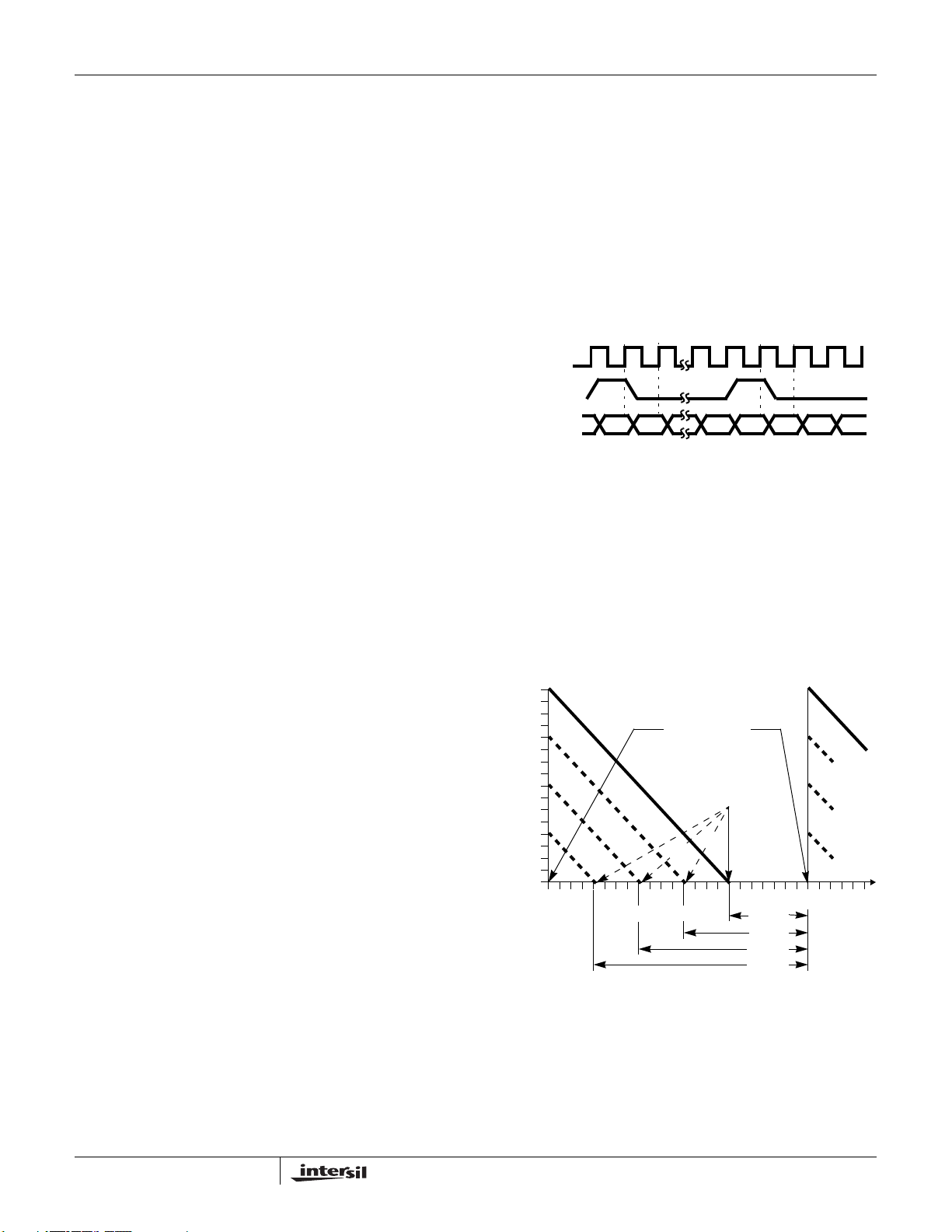
The carrier offset frequency is loaded using the COF and
COFSYN
C pins. Figure 13 details the timing relationship
between COF, COFSYNC and CLKIN. The offset frequency
wo
rd can be zeroed if it is not needed. Similarly, the
Sample Offset Frequency Register controlling the ReSampler NCO is loaded via the SOF and SOFSYNC pins.
The procedure for loading data through the two pin NCO
interfaces is identical except that the timing of SOF and
SOFSYNC is relative to PROCCLK.
CLKIN
COFSYNC/
SOFSYNC
COF/
SOF
NOTE: Data must be loaded MSB first.
FIGURE 13. SERIAL INPUT TIMING FOR COF AND SOF INPUTS
MSB
LSB
MSB
Each serial word has a programmable word width of either 8,
16
, 24, or 32-bits (See Control Word 0, Bits 4 and 5, for the
Carrier NCO programming and Control Word 11, Bits 3 and
4, for Timing NCO programming). On the rising edge of the
clock, data on COF or SOF is clocked into an input shift
register. The beginning of a serial word is designated by
asserting either COFSYNC or SOFSYNC “high” one CLK
period prior to the first data bit.
32†
30
28
26
†
24
22
20
18
†
16
14
12
10
†
8
6
SHIFT COUNTER VALUE
4
2
0
ASSERTION OF
COFSYNC, SOFSYNC
DATA TRANSFERRED
TO HOLDING REGISTER
(8)
(24)
(16)
CLK TIMES
(32)
54504642383430262218141062
T
††
D
T
††
D
T
††
D
T
††
D
† Serial word width can be: 8, 16, 24, 32 bits wide.
†† T
is determined by the COFSYNC, COFSYNC rate.
D
FIGURE 14. HOLDING REGISTERS LOAD SEQUENCE FOR
COF AND SOF SERIAL OFFSET FREQUENCY
DATA
NOTE: Serial Data must be loaded MSB first, and COFSYNC or
SOFSYNC should not be asserted for more than one
CLK cycle.
14
FN4450.4
May 1, 2007
HSP50214B
www.BDTIC.com/Intersil
NOTE: COF loading and timing is relative to CLKIN while SOF
loading and timing is relative to PROCCLK.
NOTE: T
can be 0, and the fastest rate is with 8-bit word width.
D
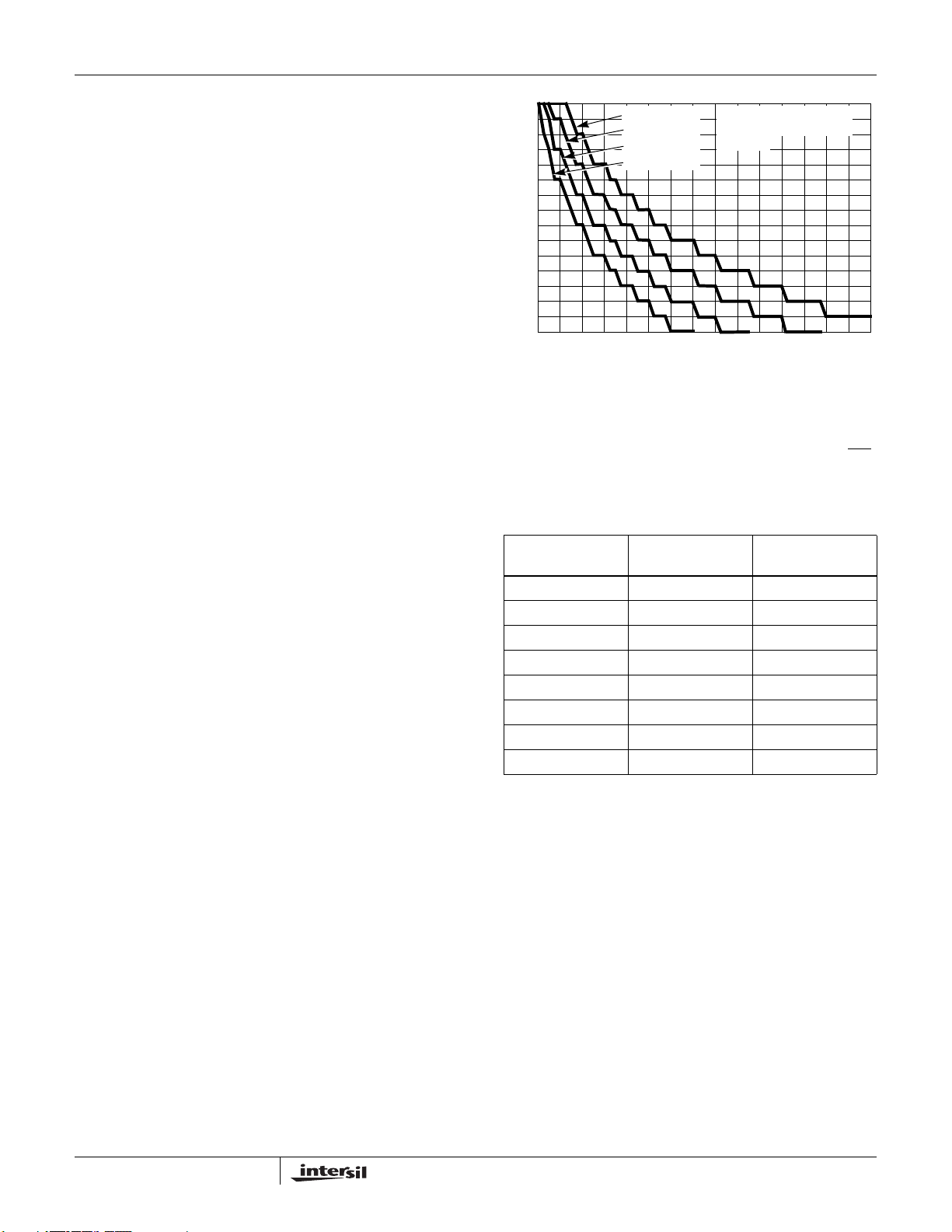
The assertion of the COFSYNC (or SOFSYNC) starts a count
down from the programmed word width. On following CLKs,
data is shifted into the register until the specified number of
bits have been input. At this point the contents of the register
are transferred from the Shift Register to the respecti ve 32-bit
Holding Register. The Shift Register can accept new data on
the following CLK. If the serial input word is defined to be less
than 32-bits, it will be transferred to the MSBs of the 32-bit
Holding Register and the LSBs of the Holding Register will be
zeroed. See Figure 14 for details.
CIC Decimation Filter
The mixer output may be filtered with the CIC filter or it may
be routed directly to the halfband filters. The CIC filter is use d
to reduce the sample rate of a wideband signal to a rate that
the halfbands and programmable filters can process, given
the maximum computation speed of PROCCLK. (See
Halfband and FIR Filter Sections for techniques to calculate
this value).
Prior to the CIC filter, the output of the
barrel shifter. The shifter is used to adjust the gain in 6dB
steps to compensate for the variation in CIC filter gain with
decimation. (See Equation 6). Fine gain adjustments must
be done in the AGC Section. The shifter is controlled by the
sum
of a 4-bit CIC Shift Gain word from the microprocessor
and a 3-bit gain word from the GAINADJ(2:0) pins. The three
bit value is pipelined to match the delay of the input samples.
The sum of the 3 and 4-bit shift gain words saturates at a
value of 15. Table 1 details the permissible values for the
GAINADJ(2:0) barrel shifter control, while Figure 15 shows
the permissible CIC Shift Gain values.
The CIC filter structure for the HSP50214B is fifth order; that
is it ha
s five integrator/comb pairs. A fifth order CIC has
84dB of alias attenuation for output frequencies below 1/8
the CIC output sample rate.
mixer goes through a
15
14
13
12
11
10
9
8
7
6
5
4
3
2
CIC SHIFT GAIN (FROM PROCESSOR)
1
0
812202836445260
FIGURE 15. CIC SHIFT GAIN VALUES
The decimation factor of the CIC
8-BIT INPUT
10-BIT INPUT
12-BIT INPUT
14-BIT INPUT
164403224 645648
DECIMATION (R)
ALLOWABLE CIC SHIFT
GAINS ARE BELOW THE
CURVES
filter is programmed in
Control Word 0, Bits 12 - 7. The C IC Shift Gain is programmed
in Control Word 0, Bits 16-13. The CIC Bypass is set in
Control Word 0, Bit 6. When bypassing the CIC filter, the
ENI
signal must be de-asserted between samples, i.e., the CL KIN
rate must be ≥ 2 • f
TABLE 3. GAIN ADJUST CONTROL AND CIC DECIMATION
VALUE
ΔGAIN
(dB) GAIN ADJ(2:0)
0 000 32
6 001 27
12 010 24
18 011 21
24 100 18
30 101 16
36 110 12
42 111 10
.
S
MAX. CIC
DECIMATION
CIC Gain Calculations
The gain through the CIC filter increases with increased
decimation. The programmable barrel shifter that precedes
the first integrator in the CIC is used to offset this variation.
Gain variations due to decimation should be offset using the
4-bit CIC Shift Gain word. This allows the input signal level to
be adjusted in 6dB steps to control the CIC output level.
The gain at each stage of the CIC is:
kRN,=
where R is the decimation factor and N is the number of stages.
Th
e input to the CIC from the mixer is 15-bits, and the bit widths
of the accumulators for the five stages in the HSP50214B are
40, 36, 32, 32, and 32, as shown in Figure 16. This limits the
maximum decimation in the CIC to 32 for a full scale input.
If R is 32, the gain through all five integrator stages is 32
(The gain through the last four CIC stages is 2
15
20
, through the
May 1, 2007
(EQ. 6)
5
= 225.
FN4450.4

HSP50214B
www.BDTIC.com/Intersil
last 3 it is 215, etc.). The sum of the input bits and the growth
bits cannot exceed the accumulator size. This means that for a
decimation of 32 and 15 input bits, the first accumulator must
be 15 + 25 = 40-bits.
Thus, the value of the CIC Shift Gain word can be
calcul
ated:
SG = FLOOR 39 - [ IIN() - log
NOTE: The number of input bits is IIN. (If the number of bits into
the CIC filter is used, the value 40 replaces 39).
(R)5 for 4<R<32
2
for R = 4= 15
(EQ. 7)
For 14-bits, Equation 7 becomes:
SG FLOOR 25 log
15= for R 4=
R()5]for 4 R 32<<–[=
2
(EQ. 8A)
For 12-bits, Equation 7 becomes:
SG FLOOR 27 log
15= for 4 R 5≤≤
R()5]for 5 < R < 40–[=
2
(EQ. 8B)
For 10-bits, Equation 7 becomes:
SG FLOOR 29 log
R()5]for 6 < R < 52–[=
2
for 4 R 6≤≤15=
(EQ. 8C)
The CIC filter decimation counte
r can be loaded synchronous
with other PDC chips, using the SYNCIN1 signal and the CIC
External Sync Enable bit. The CIC external Sync Enable is set
via Control Word 0, Bit 19.
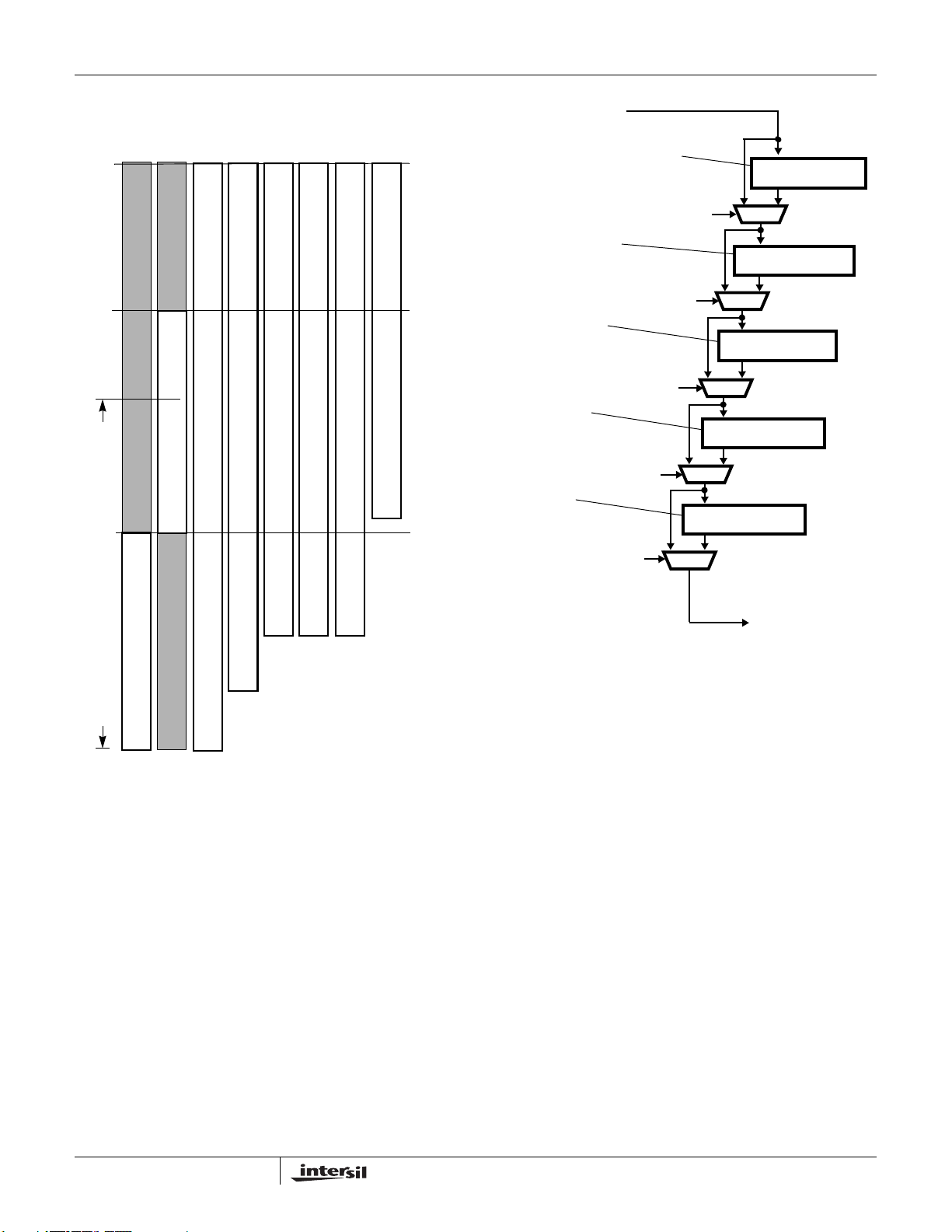
Halfband Decimating Filters
The Programmable Down Converter has five halfband filter
stages, as shown in Figure 17. Each stage decimates by 2
and filters out half of the available bandwidth. The first
ha
lfband, or HB1, has 7 taps. The remaining halfbands;
HB2, HB3, HB4, and HB5; have 11, 15, 19, and 23 taps
respectively. The coefficients for these halfbands are given
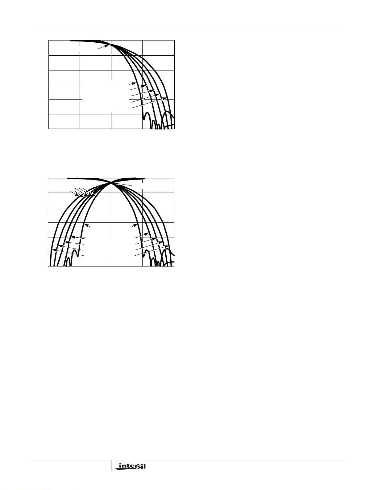
in Table 4. Figure 18 shows the frequency response of each
of the halfband filters with respect to normalized frequency,
F
. Frequency normalization is with respect to the input
N
sampling frequency of each filter section. Each stage is
activated by their respective bit location (15-20) in Control
Word 7. Any combination of halfband filters may be used, or
all may be bypassed.
For 8-bits, Equation 7 becomes:
SG FLOOR 31 log
15= for 4 R 9≤≤
Figure 15 is a plot of Equations 8A throug
R()5]for 9 < R < 64–[=
2
(EQ. 8D)
h 8D. The 4-bit CIC
Shift Gain word has a range from 0 to 15. The 6-bit
Decimatio
n Factor counter preload field, (R-1), has a range
from 0 to 63, limited by the input resolution as cited above.
Using the Input Gain Adjust Control Signals
The input gain offset control GAINADJ(2:0)) is provided to
offset the signal gain through the part, i.e., to keep the CIC
filter output level constant as the analog front end
attenuation is changed. The gain adjust offset is 6dB per
code, so the gain adjust range is 0 to 42dB. For example, if
12dB of attenuation is switched in at the receiver RF front
end, a code of 2 would increase the gain at the input to the
CIC filter up 12dB so that the CIC filter output would not drop
by 12dB. This fixed gain adjust eliminates the need for the
software to continually normalize.
One must exercise care when using this function as it can
cause ove
shifter from the gain adjust control signals is the equivalent
of an extra bit of input. The maximum decimation in the CIC
is reduced accordingly. With a decimation of 32, all 40-bits of
the CIC are needed, so no input offset gain is allowed. As
the decimation is reduced, the allowable offset gain
increases. Table 3 shows the decimation range versus
desired offset gain range. T able 3 assumes that the CIC Shift
Gain has been programmed per Equation 7 or 8A.
rflow in the CIC filter. Each gain adjust in the
16
FN4450.4
May 1, 2007
OUTPUT SHIFTER BITS TAKEN WHEN CIC IS BYPASSED
-
www.BDTIC.com/Intersil
HSP50214B
HALFBAND
FILTER INPUT
f
= fS
1
F
HB1
= F
HB2
OR F
HB4
IN
= fS OR fS/2
OR F
HB1
†
OR F
HB2
†
/2
HB3
†
/2
HB1
/2
†
†
/2
= F
HB1
HB2
SECTION
FN = f
S
HALFBAND FILTER 4
0
HALFBAND FILTER 5
0
1
F
= F
5
HALFBAND FILTER 1
0
HALFBAND FILTER 2
0
1
F
HB2
HALFBAND FILTER 3
0
1
F
= F
HB3
1
F
= F
HB4
HB3
OR F
HB4
HALFBAND
FILTER OUTPUT
-1
-2
-3
-4
-5
-6
-7
-8
-9
-10
-11
-12
-13
-14
-15
-16
-17
-18
-19
-20
-21
-22
-23
-24
-25
-26
-27
-28
-29
-30
-31
ACC5
CIC
OUTPUT
0
-1
2
-2
2
-3
2
-4
2
-5
2
-6
2
-7
2
-8
2
-9
2
-10
2
-11
2
-12
2
-13
2
-14
2
-15
2
-16
2
-17
2
-18
2
-19
2
-20
2
-21
2
-22
2
-23
2
CONTROL WORD 7, BIT 18
F
CONTROL WORD 7, BIT 15
F
N
CONTROL WORD 7, BIT 16
= F
F
N
CONTROL WORD 7, BIT 17
FN = F
HB3
= F
N
HB4
CONTROL WORD 7, BIT 19
† Each halfband section decimates by 2.
FIGURE 17. BLOCK DIAGRAM OF HALFBAND FILTER
INPUT
(SHFT=0)
(SHFT=15)
0
-1
2
-2
2
-3
2
-4
2
-5
2
-6
2
-7
2
-8
2
-9
2
-10
2
-11
2
-12
2
-13
2
-14
2
0
-1
2
-2
2
-3
2
-4
2
-5
2
-6
2
-7
2
-8
2
-9
2
-10
2
-11
2
-12
2
-13
2
-14
2
2
2
2
2
2
2
2
2
ACC2
ACC3
ACC4
0
0
0
0
-1
-1
2
-2
2
-3
2
-4
2
-5
2
-6
2
-7
2
-8
2
-9
2
-10
2
-11
2
-12
2
-13
2
-14
2
-15
2
-16
2
-17
2
-18
2
-19
2
-20
2
-21
2
-22
2
-23
2
-24
2
-25
2
-26
2
-27
2
-28
2
-29
2
-30
2
-31
2
-32
-33
-34
-35
-36
-37
-38
-39
-1
2
2
-2
-2
2
2
-3
-3
2
2
-4
-4
2
2
-5
-5
2
2
-6
-6
2
2
-7
-7
2
2
-8
-8
2
2
-9
-9
2
2
-10
-10
2
2
-11
-11
2
2
-12
-12
2
2
-13
-13
2
2
-14
-14
2
2
-15
-15
2
2
-16
-16
2
2
-17
-17
2
2
-18
-18
2
2
-19
-19
2
2
-20
-20
2
2
-21
-21
2
2
-22
-22
2
2
-23
-23
2
2
-24
-24
2
2
-25
-25
2
2
-26
-26
2
2
-27
-27
2
2
-28
-28
2
2
-29
-29
2
2
-30
-30
2
2
-31
-31
2
2
-32
2
-33
2
-34
2
-35
2
0
-1
2
2
-2
2
2
-3
2
2
-4
2
2
-5
2
2
-6
2
2
-7
2
2
-8
2
2
-9
2
2
-10
2
2
-11
2
2
-12
2
2
-13
2
2
-14
2
2
-15
2
2
-16
2
2
-17
2
2
-18
2
2
-19
2
2
-20
2
2
-21
2
2
-22
2
2
-23
2
2
-24
2
2
-25
2
2
-26
2
2
-27
2
2
-28
2
2
-29
2
2
-30
2
2
-31
2
2
ACC1
INPUT
NOTE: If 14 input bits are not needed, the gain adjust can be in
creased by one for each bit that the input is shifted down
at the input. For example, if only 12-bits are needed, an
offset range of 24dB is possible for a decimation of 24.
FIGURE 16. CIC FILTER BIT WEIGHTING
Since each halfband filter section decimates by 2, the total
decimation through the halfband filter is given by:
DECHB2N=
(EQ. 9)
where N = Number of Halfband Filters Selected (1 - 5).
17
FN4450.4
May 1, 2007
0
www.BDTIC.com/Intersil
-20
-40
HSP50214B
-6dB BANDWIDTH
-60
-80
MAGNITUDE (dB)
-100
-120
HALFBAND FILTER 5
HALFBAND FILTER 4
HALFBAND FILTER 3
HALFBAND FILTER 2
HALFBAND FILTER 1
0.125 0.25 0.375 0.5
NORMALIZED FREQUENCY (FN)
FIGURE 18. HALFBAND FILTER FREQUENCY RESPONSE
0
ALIAS
PROFILES
-20
-40
-60
-80
MAGNITUDE (dB)
-100
-120
HALFBAND FILTER 5
HALFBAND FILTER 4
HALFBAND FILTER 3
HALFBAND FILTER 2
HALFBAND FILTER 1
0.125 0.25 0.375 0.5
NORMALIZED FREQUENCY (FN)
-6dB BANDWIDTH
FIGURE 19. HALFBAND FILTER ALIAS CONSIDERATIONS
18
FN4450.4
May 1, 2007
HSP50214B
www.BDTIC.com/Intersil
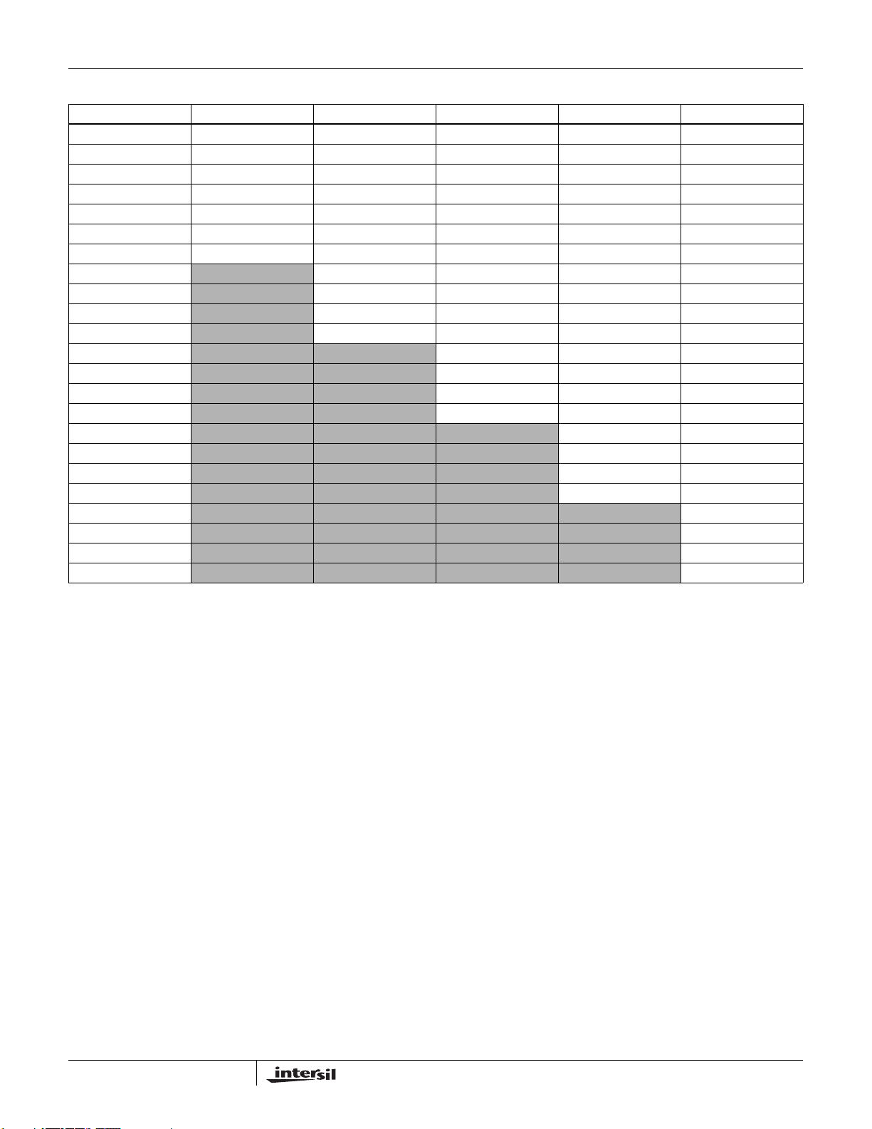
TABLE 4. HALFBAND FILTER COEFFICIENTS
COEFFICIENTS HALFBAND #1 HALFBAND #2 HALFBAND #3 HALFBAND #4 HALFBAND #5
C0 - 0.031303406 0.005929947 -0.00130558 0.000378609 -0.000347137
C1 0.000000000 0.000000000 0.000000000 0.000000000 0.000000000
C2 0.281280518 -0.049036026 0.012379646 -0.003810883 0.00251317
C3 0.499954224 0.000000000 0.000000000 0.000000000 0.000000000
C4 0.281280518 0.29309082 -0.06055069 0.019245148 -0.010158539
C5 0.000000000 0.499969482 0.000000000 0.000000000 0.000000000
C6 - 0.031303406 0.29309082 0.299453735 -0.069904327 0.03055191
C7 0.000000000 0.499954224 0.000000000 0.000000000
C8 -0.049036026 0.299453735 0.304092407 -0.081981659
C9 0.000000000 0.000000000 0.500000000 0.000000000
C10 0.005929947 -0.06055069 0.304092407 0.309417725
C11 0.000000000 0.000000000 0.500000000
C12 0.012379646 -0.069904327 0.309417725
C13 0.000000000 0.000000000 0.000000000
C14 -0.00130558 0.019245148 -0.081981659
C15 0.000000000 0.000000000
C16 -0.003810883 0.03055191
C17 0.000000000 0.000000000
C18 0.000378609 -0.010158539
C19 0.000000000
C20 0.00251317
C21 0.000000000
C22 -0.000347137
NOTE: While Halfband filters are typically selected starting with the last stage in the filter chain to give the maximum alias free ban
a higher throughput rate may be obtained using other filter combinations. See Application Note 9720, “Calculating Maximum
Processing Rates of the PDC”.
dwidth,
Depending on the number of halfbands used, PROCCLK
must operate at a minimum rate above the input sample
rate, f
, to the halfband. This relationship depends on the
S
number of multiplies for each of the halfband filter stages.
The filter calculations take 3, 4, 5, 6, and 7 multiplies per
input for HB1, HB2, HB3, HB4, and HB5 respectively. If we
keep the assumption that f
is the input sampling frequency,
S
then Equation 10 shows the minimum ratio needed.
)+
)+
HB5
)+
)+
)]/2T
(EQ. 10)
f
PROCCLK/fS
(6)(HB4)(2
(5)(HB3)(2
(4)(HB2)(2
(3)(HB1)(2
(HB4 + HB5)
(HB3+HB4+HB5)
(HB2+HB3+ HB4+HB5)
(HB1+HB2+HB3+HB4+HB5)
≥ ([(7)(HB5)(2
where
HB1 = 1 if this section is selected and 0 if it is bypassed;
HB2 = 1 if this section is selected and 0 if it is bypassed;
HB3 = 1 if this section is selected and 0 if it is bypassed;
HB4 = 1 if this section is selected and 0 if it is bypassed;
HB5 = 1 if this section is selected and 0 if it is bypassed;
T = number of Halfband Filters Selected. Th
e range for T is
from 0 to 5.
19
Examples of PROCCLK Rate Calculations
Suppose we enable HB1, HB3, and HB5. Using Figure 16,
HB1= 1, HB3 = 1, and HB5 = 1. Since stage 2 and stage 4
are no
t used, HB2 and HB4 = 0. PROCCLK must operate
faster than (7x2+5x4+3x8)/8 = 7.25 times faster than f
.
S
If all five halfbands are used, then PROCCLK must operate at
(7x2+6x4+5x8+4x16+3x32)/32 = 7.4375 times faster than f
S
255-Tap Programmable FIR Filter
The Programmable FIR filter can be used to implement real
filters with even or odd symmetry, using up to 255 filter taps,
or complex filters with up to 64 taps. The FIR filter takes
advantage of symmetry in coefficients by summing data
samples that share a common coefficient, prior to
multiplication. In this manner, two filter taps are calculated
per multiply accumulate cycle. Asymmetric filters cannot
share common coefficients, so only one tap per multiply
accumulate cycle is calculated. The filter can be effectively
bypassed by setting the coefficient C
coefficients, C
= 0.
N
= 1 and all other
0
FN4450.4
May 1, 2007
.

HSP50214B
www.BDTIC.com/Intersil
Additionally, the Programmable FIR filter provides for
decimation factors, R, from 1 to 16. The processing rate of
the Filter Compute Engine is PROCCLK. As a result, the
frequency of PROCCLK must exceed a minimum value to
ensure that a filter c alculatio n is complete before the result is
required for output. In configurations which do not use
decimation, one input sample period is available for filter
calculation before an output is required. For configurations
which employ decimation, up to 16 input sample periods
may be available for filter calculation.
For real filter configurations, use Equatio
calculate the number of taps availabl
sample rate.
TAPS floor PROCCLK F
SYM) SYM()ODD#()[]–
SAMP
for real filters, and
TAPS floor (PROCCLK F
SAMP
for complex filters, where floor is defined as the integer
portion
of a number; PROCCLK is the compute clock; f
= the FIR input sample rate; R = Decimation Factor; SYM =
1 for symmetrical filter, 0 for asymmetrical filter; ODD# = 1
for an odd number of filter taps, 0 = an even number of taps.
Use Equation 12A to calculate the maximum input rate.
F
SAMP
PROCCLK() R() R floor Taps()[[+[⁄ +=
SYM()ODD#()]1 SYM+()⁄]]
for real filters, and
F
SAMP
PROCCLK()R()[]R floor Taps()2()][+[]⁄=
for complex filters, where floor[x], PROCCLK, f
Decimation Factor, SYM, and ODD# are defined as in
Equation 11A.
Use Equation 13 to calculate the maximum output sample
rate for both real and complex
F
FIROUT
F
()R⁄=
SAMP
filters.
The coefficients are 22-bits and are loaded using writes to
Con
trol Words 128 through 255 (see Microprocessor Write
Section). For real filters, the same coefficients are used by I
and Q paths. If the filter is configured as a symmetric filter
using Control Word 17, Bit 9, then coefficients are loaded
starting with the center coefficient in Control Word 128 and
proceeding to last coefficient in Control Word 128+n. The
filter symmetry type can be set to even or odd symmetric,
and the number of filter coefficients can be even or odd, as
illustrated in Figure 20. Note that complex filters can also be
realized but are only allowed to be asymmetric. Only the
coef
ficients that are used need to be loaded.
ns 1 1A an d 11B to
e at a given input filter
S AMP
(EQ. 11A)
(EQ. 11B)
S AMP
(EQ. 12A)
(EQ. 12B)
, R =
(EQ. 13)
R⁄()⁄ R]–[()1 +(=
R⁄()⁄ R) 2]⁄–[=
I
E
N
T
COEFFICIENT VALUE COEFFICIENT VALUE
COEFFICIENT VALUE
V
A
C0
ODD SYMMETRIC
EVEN TAP FILTER
C0
ODD SYMMETRIC
ODD TAP FILTER
C0
ASYMMETRIC
ODD TAP FILTER
C
C
I
L
U
E
C0
COEFFICIENT VALUECOEFFICIENT VALUE
EVEN SYMMETRIC
EVEN TAP FILTER
C0
EVEN SYMMETRIC
ODD TAP FILTER
C0
COEFFICIENT VALUE
ASYMMETRIC
EVEN TAP FILTER
C
IMAGINARY
COEFFICIENT
R
CN-1
CN-1
Q
C
VALUE
Q(0)
E
A
L
COEFFICIENT
NUMBER
CN-1
COEFFICIENT
NUMBER
COEFFICIENT
NUMBER
REAL FILTERS
C
I(0)
C
O
E
F
F
I
C
COMPLEX FILTERS
CN-1
Q(N-1)
COEFFICIENT
NUMBER
C
I(N-1)
CN-1
COEFFICIENT
NUMBER
CN
COEFFICIENT
NUMBER
COEFFICIENT
NUMBER
Definitions:
Even Symmetric: h(n) = h(N-n-1) for n = 0 to N-1
Odd Symmetric: h(n) = -h(N-n-1) for n = 0 to N-1
Asymmetric: A filter with no coefficient symmetry.
Even Tap filter: A filter where N is an even number.
Odd Tap filter: A filter where N is an odd number.
Real Filter: A filter implemented with real coefficients.
Complex Filters: A filter with quadrature coefficients.
FIGURE 20. DEMONSTRATION OF DIFFERENT TYPES OF
DIGITAL FIR FILTERS CONFIGURED IN THE
PROGRAMMABLE DOWNCONVERTER
Automatic Gain Control (AGC)
The AGC Section provides gain to small signals, after the
large signals and out-of-band noise have been filtered out, to
ensure that small signals have sufficient bit resolution in the
Resampling/Interpolating Halfband filters and the Output
Formatter. The AGC can also be used to manually set the
gain. The AGC optimizes the bit resolution for a variety of
input amplitude signal levels. The AGC loop automatically
adds gain to bring small signals from the lower bits of the 26bit programmable FIR filter output into the 16-bit range of the
20
FN4450.4
May 1, 2007

HSP50214B
www.BDTIC.com/Intersil
output section. Without gain control, a signal at -72dBFS =
20log
-12
(2
) at the input would have only 4-bits of
10
resolution at the output (12-bits less than the full scale
16-bits). The potential increase in the bit resolution due to
processin
g gain of the filters can be lost without the use of
the AGC.
Figure 23 shows the Block Diagram for the AGC Section.
The FIR filter data output is routed
to the Resampling and
Halfband filters after passing through the AGC multipliers
and Shift Registers. The outputs of the Interpolating
Halfband filters are routed to the Cartesian to Polar
coordinate converter. The magnitude output of the
coordinate converter is routed through the AGC error
detector, the AGC error scaler and into the AGC loop filter.
This filtered error term is used to drive the AGC multiplier
and shifters, completing the AGC control loop.
The AGC Multiplier/Shifter portion
of the AGC is identified in
Figure 23. The gain control from the AGC loop filter is
sampled when new data enters the Multiplier/Shifter. The
limit
detector detects overflow in the shifter or the multiplier
and saturates the output of I and Q data paths
independently. The shifter has a gain from 0 to 90.31dB in
6.021dB steps, where 90.31dB = 20log
(2N), when N = 15.
10
The mantissa provides an additional 6dB of gain in
0.0338dB steps where 6.0204dB = 20log
where X = 2
15
-1. Thus, the AGC multiplier/shifter transfer
[1+(X)2
10
-15
],
function is expressed as:
AGC Mult/Shift Gain 2
N
1X()2
15–
],+[=
(EQ. 14)
where N, the shifter exponent, has a range of 0<N<15 and X,
th
e mantissa, has a range of 0<X<(2
15
-1).
Equation 14 can be expressed in dB,
(AGC Mult/Shift Ga
in)dB 20log
2N1X()2
10
-15
]+[()=
(EQ. 14A)
The full AGC range of the Multiplier/Shifter is from 0 to
96.33
1dB (20log
[1+(215-1)2
10
-15
] + 20log10[215] = 96.331).
Figure 21 illustrates the transfer function of the AGC
multiplier versus mantissa control for N = 0. Figure 22
illustrates the complete AGC Multiplier/Shifter Transfer
fu
nction for all values of exponent and mantissa control.
6
5
4
3
2
GAIN - LINEAR AND dB
1
0
0 16 32 48 64 80 96 112 128 144 160 176 192 208 224 240
AGC CONTROL MANTISSA VALUES (TIMES 256)
FIGURE 21. AGC MULTIPLIER LINEAR AND dB TRANSFER
FUNCTION
100
90
80
70
60
50
GAIN (dB)
40
30
20
10
0
064 128 192
AGC CONTROL WORD (MANTISSA x 256)
FIGURE 22. AGC GAIN CONTROL TRANSFER FUNCTION
G (dB)
G (LINEAR)
N = 15
N = 14
N = 13
N = 12
N = 11
N = 10
N = 9
N = 8
N = 7
N = 6
N = 5
N = 4
N = 3
N = 2
N = 1
N = 0
The Cartesian to Polar Coordinate converter accepts I and Q
data and generates magnitude and phase data. The
magnitude output is determined by the Equation 15:
The resolution of the mantissa was increased to 16-bits in
t
he A Version, to provide a theoretical AM modulation level
of -96dBc (depending on loop gain, settling mode and SNR).
This effectively eliminates AM spurious caused by the AGC
resolution.
For fixed gains, either set the upper and lower AGC limits to
th
e same value, or set the limits to minimum and maximum
gains and set the AGC loop gain to zero.
r 1.64676 I
where the magnitude limits are determined by the maximum
I
and Q signal levels into the Cartesian to Polar converter.
Taking fractional 2’s complement representation, magnitude
ranges from 0 to 2.329, where the maximum output is
r 1.64676 1.0()21.0()
The AGC loop feedback path consists of an error detector, error
scali
ng, and an AGC loop filter. The error detector subtracts the
magnitude output of the coordinate converter from the
programmable AGC THRESHOLD value. The bit weighting of
21
2Q2
+ .=
2
+= 1.64676 1.414× 2.329==
(EQ. 15)
.
FN4450.4
May 1, 2007

HSP50214B
www.BDTIC.com/Intersil
the AGC THRESHOLD value (Control Word 8, Bits 16-28) is
shown in T able 5. Note that the MSB is always zero. The range
of the AGC THRESHOLD value is 0 to +3.9995. The AGC
Erro
r Detector output has the identical range.
TABLE 5. AGC THRESHOLD (CONTROL WORD 8) BIT
28 27 26 25 24 23 22 21 20 19 18 17 16
22120
2
WEIGHTING
-12-22-32-42-52-62-72-82-92-10
. 2
The loop gain is set in the AGC Error Scaling circuitry, using
the two programmable mantissas and exponents. The
mantissa, M, is a 4-bit value which weights the loop filter
input from 0.0 to 0.9375. The exponent, E, defines a shift
0
factor that provides additional weighting from 2
to 2
-15
.
Together the mantissa and exponent define the loop gain as
given by,
AGC Loop Gain M
where M
E
is a 4-bit binary value ranging from 0 to 15. Table 7 and
LG
=
LG
is a 4-bit binary value ranging from 0 to 15 , an d
LG
8 detail the binary values and th
24–2
15 ELG–()–
e resulting scaling effects of
(EQ. 16)
the AGC scaling mantissa and exponent. The composite
(shifter and multiplier) AGC scaling Gain range is from
0.0000 to 2.329(0.9375)
0
2
= 0.0000 to 2.18344. The scaled
gain error can range (depending on threshold) from 0 to
2.18344, which maps to a “gain change per sample” range of
0 to 3.275dB/sample.
The AGC Gain mantissa and exponent values are
prog
rammed into Control Word 8, Bits 0-15. The PDC
provides for the storing of two values of AGC Scaling Gain
(both exponent and mantissa). This allows for quick
adjustment of the loop gain by simply asserting the external
control line AGCGNSEL. When AGCGNSEL = 0, then AGC
GAIN 0 is selected, and when AGCGNSEL = 1, AGC Loop
Gain 1 is selected. Possible applications include
acquisition/tracking, no burst present/burst present, strong
signal/weak signal, track/hold, or fast/slow AGC values.
The AGC loop filter consists of an accumulator with a built in
limiting function. The
maximum and minimum AGC gain
limits are provided to keep the gain within a specified range
and are programed by 12-bit Control Words using Equation 17:
AG
C Gain Limit 1 m
AGC Gain Limit()dB = 6.02()eeee()20 1.0 0.mmmmmmmm+()log+
+()2
=
AGC
2
e
(EQ. 17)
(EQ. 17A)
9–
where m is an 8-bit mantissa value between 0 and 255, and e
is the 4-bit expon
ent ranging from 0 to 15. Control Word 9,
Bits 16-27 are used for programmin g the upper limit, while bits
0-11 are used to program the lower threshold. The range s and
format for these limit values are shown in Tables 6A through
6C. The bit weightings for the AGC Loop Feedback elements
are detailed in Table 9A.
TABLE 6A. AGC LIMIT EXPONENT vs GAIN
GAIN(dB) EXPONENT MANTISSA
96.332 15 255
90.309 15 0
84.288 14 0
78.268 13 0
72.247 12 0
66.227 11 0
60.206 10 0
54.185 9 0
48.165 8 0
42.144 7 0
36.124 6 0
30.103 5 0
24.082 4 0
18.062 3 0
12.041 2 0
6.021 1 0
0.000 0 0
TABLE 6B. AGC LIMIT MANTISSA vs GAIN
GAIN(dB) EXPONENT MANTISSA
6.000 0 255
5.750 0 240
5.500 0 226
5.250 0 212
5.000 0 199
4.750 0 185
4.500 0 173
4.250 0 161
4.000 0 149
3.750 0 138
3.500 0 127
3.250 0 116
3.000 0 105
2.750 0 95
2.500 0 85
2.250 0 75
2.000 0 66
1.750 0 57
1.500 0 48
1.250 0 39
1.000 0 31
0.750 0 23
0.500 0 15
0.250 0 7
0.020 0 1
22
FN4450.4
May 1, 2007

HSP50214B
www.BDTIC.com/Intersil
TABLE 6C. AGC LIMIT DATA FORMAT
CONTROL WORD 9 BIT: 27 26 25 24 23 22 21 20 19 18 17 16
FORMAT e e e e m m m m m m m m
SERIAL
OUT
μP
(11 MANTISSA
4 EXPONENT)
AGC LOOP FILTER
REGISTER
AGC
LOAD
M
U
X
MANTISSA =
16
01.XXXXXXXXXXXXXX
16
MSB = 0
16
REGISTER
MSB = 0
4
EXP=2
EN
20
NNNN
μP
(RANGE = -2.18344 TO 2.18344)
+
LIMITER
LIMIT
DET
UPPER LIMIT
LOWER LIMIT †
LIMIT
DET
†
AGC ERROR SCALING
13
EXP
AGCGNSEL
EXP †
†
LOOP GAIN 0
MAN
SHIFT
MANTISSA
4
4
AGC REGISTER 0
AGC REGISTER 1
MAGNITUDE
(RANGE = 0 TO 2.3)
(RANGE = 0 TO 1)
† EXP †
MAN
LOOP GAIN 1
AGC
ERROR
DETECTOR
13
Δ
(S = 0)
UNSIGNED †
THRESHOLD
STT.TTTTTTTTTT
IFIR
QFIR
26
26
18
SHIFTER
18
SHIFTER
AGC MULTIPLIER/SHIFTER
LIMITER
LIMIT
DET
† Controlled via microprocessor interface.
FIGURE 23. AGC BLOCK DIAGRAM
Using AGC loop gain, the AGC range, and expected error
detector output, the gain adjustments per output sample for
the Loop Filter Section of the Digital AGC can be given by:
AGC Slew Rate 1.5dB THRESH MA G*1.64676())×–(=
M
()24–()2
LG
⎛⎞
⎝⎠
15 ELG–()–
(EQ. 18)
18
IAGC
QAGC
LIMITER
RESAMPLING
FIR FILTERS
AND
INTERPOLATING
HALFBAND
FILTERS
18
CARTESIAN
TO
POLAR
COORDINATE
CONVERTER
(G = 1.64676)
The loop gain determines the growth rate of the sum in the
lo
op accumulator which, in turn, determines how quickly the
AGC gain traces the transfer function given in Figures 21
and 22. Since the log of the gain response is roughly linear,
the loop response can be appro
ximated by multiplying the
maximum AGC gain error by the loop gain. The expected
23
FN4450.4
May 1, 2007

HSP50214B
www.BDTIC.com/Intersil
range for the AGC rate is ~ 0.000106 to 3.275dB/output
sample time for a threshold of 1/2 scale. See the notes at the
bottom of Table 9A for calculation of the AGC response
times. The maximum AGC Response is given by:
AGC Response
Input(Cart/Polar Gain)(Error Det Gain) AGC(=
Max
Loop Gain)(AGC Output Weighting)
(EQ. 19)
Since the AGC error is scaled to adjust the gain, the loop
settl
es asymptotically to its final value. The loop settles to
the mean of the signal.
TABLE 7. AGC LOOP GAIN BINARY MANTISSA TO GAIN
SCALE FACTOR MAPPING
BINARY
DE
CO
(MMMM)
0000 0.0000 1000 0.5000
0001 0.0625 1001 0.5625
0010 0.1250 1010 0.6250
0011 0.1875 1011 0.6875
0100 0.2500 1100 0.7500
0101 0.3125 1101 0.8125
0110 0.3750 1110 0.8750
0111 0.4375 1111 0.9375
TABLE 8. AGC LOOP GAIN BINARY EXPONENT TO GAIN
BINARY
DE
CO
(EEEE)
0000 2
0001 2
0010 2
0011 2
0100 2
0101 2
0110 2
0111 2
SCALE
FA
CTOR
SCALE FACTOR MAPPING
SCALE
CTOR
FA
15
14
13
12
11
10-
9
8
BINARY
DE
CO
(MMMM)
BINARY
DE
CO
(EEEE)
1000 2
1001 2
1010 2
1011 2
1100 2
1101 2
1110 2
1111 2
SCALE
FA
CTOR
SCALE
CTOR
FA
7
6
5
4
3
2
1
0
when AGCGNSEL = 0, and selecting Gain 1 when
AGCGNSEL = 1.
In the HSP50214, a reset event (caused by SYNCIN2 or
CW
25) would clear the AGC loop filter accumulator. In the
HSP50214B, if Control Word 27, Bit 15 is set to zero, the
AGC loop filter accumulator will clear as in the original
HSP50214. If Control Word 27, Bit 15 is set to a one, the
backend reset (from CW25) will not clear the AGC loop filter
accumulator.
In the HSP50214, the settling mode of the AGC forces the
mean
of the signal magnitude error to zero. The gain error is
scaled and used to adjust the gain up or down. This
proportional scaling mode causes the AGC to settle to the
final gain value asymptotically. This AGC settling mode is
preferred in many applications because the loop gain
adjustments get smaller and smaller as the loop settles,
reducing any AM distortion caused by the AGC.
With this AGC settling mode, the proportional gain error
cause
s the loop to settle more slowly if the threshold is
small. This is because the maximum value of the threshold
minus the magnitude is smaller. Also, the settling can be
asymmetric, where the loop may settle faster for “over
range” signals than for “under range” signals (or vice versa).
In some applications, such as burst signals or TDMA signals,
a very fast settli
ng time and/or a more predictable settling
time is desired. The AGC may be turned off or slowed down
after an initial AGC settling period.
To minimize the settling time, a median AGC settling mode
ha
s been added to the HSP50214B. This mode uses a fixed
gain adjustment with only the direction of the adjustment
controlled by the gain error. This makes the settling time
independent of the signal level.
For example, if the loop is set to adj
ust 0.5dB per output
sample, the loop gain can slew up or down by 16dB in 16
symbol times, assuming a 2 samples per symbol output
sample rate. This is called a median settling mode because
the loop settles to where there is an equal number of
magnitude samples above and below the threshold. The
disadvantage of this mode is that the loop will have a wander
(dither) equal to the programmed step size. For this reason,
it is advisable to set one loop gain for fast settling at the
beginning of the burst and the second loop gain for small
adjustments during tracking.
For example, if MLG = 0101 and ELG = 1100 , the AGC Loop
Gain = 0.3125*2
-7
. The loop gain mantissas and exponents
are set in the AGC Loop Parameter Control Register (Control
Word 8, Bits 0-15).
Two AGC loop gains a re provided in the Programmable Dow n
C
onverter, for quick adjustment of the AGC loop. The AGC
Gain select is a control input to the device, selecting Gain 0
The median settling mode is enabled by setting Control
W
ord 27, Bit 16 to a logic one. If Control Word 27, Bit 16 is
zero, the mean loop settling mode is selected and the loop
works identically to the HSP50214.
In the median mode, the loop works as follows:
The sign of the true gain error selects a fixed gain error of
00
10000000000
24
or 1110000000000b.
b
FN4450.4
May 1, 2007

HSP50214B
www.BDTIC.com/Intersil
These gain error values are scaled by the programmable
AGC loop gains to adjust the data path gain.
The maximum slew rate is ~1.5dB per output sample. See
Equa
tion 18.
In order to fully evaluate the dynamic range of the PDC,
T
able 9B is provided, which details the bit weighting from the
input to the AGC Multiplier.
Re-Sampler/Halfband Filter
The re-sampler is an NCO controlled polyphase filter that
allows the output sample rate to have a non-integer
relationship to the input sa mple rate. The f ilter engine can be
viewed conceptually as a fixed interpolation filter, followed by
an NCO controlled decimator.
The prototype polyphase filter has 192
times the input sample rate. Each of the 32 phases has 6
filter taps (6)(32) = 192. The stopband attenuation of the
prototype filter is greater than 60dB, as shown in Figure 24.
The signal to total image power ratio is approximately 55dB,
due
to the aliasing of the interpolation images. The filter is
capable of decimation factors from 1 to 4. If the output is at
least 2x the baud rate, the 32 interpolation phases yield an
effective sample rate of 64x the baud rate or approximately
1.5%, (1/64), maximum timing error.
Following the Re-sampler are two interpolation halfband
fi
lters. The halfband filters allow the user to up-sample by 2
or 4 to recover time resolution lost by decimating.
Interpolating by 2 or 4 gives 1/4 or 1/8 baud time resolution
(assuming 2x baud at the re-sampler output). The halfband
filters use the same coefficients as HB3 and HB5 from the
Halfband Filters Section. If one halfband is used, the 23-tap
filter is chosen. If two are used, the 23-tap filter runs first
taps designed at 32
followed by the 15-tap filter operating at twice the first
halfband’s rate. The 23-tap filter requires 7 multiplies, and
the 15-tap filter requires 5 multiplies to complete a filter
calculation.
Using the interpolation halfband filters allows for reduction in
the FIR fi
lter sample rate. This optimizes the use of the
programmable FIR filter by allowing the FIR output sample
rate to be closer to the Nyquist rate of the desired bandwidth.
Optimizing the FIR filter performance provides better use of
the programmable FIR taps. Table 10 details the maximum
clocking rates for the possible resampling and interpolation
ha
lfband filter configurations of this section of the PDC.
Control Word 16, Bits 2-0 identify the filter configuration.
Control Word 16, Bit 3 is used to by pass the polyphase resampler filter.
For proper data output from the inte
rpolation filters, the data
ready signal must account for the interpolation process.
Figure 25 illustrates the insertion of additional data ready
pulses to provide sufficient pulses for the new output sample
rate.
The Re-sampler Output Pulse Delay parameter is set in
Control Word 16, Bits 4-1 1. These bits set the delay between
the output samples when interpolation is utilized. Program
this distance between pulses using
()1]–[=
Nf
PROCCLK/fOUT
(EQ. 20)
A value of at least 5 is required to have sufficient time to
upd
ate the Output Buffer Register. (Writing 5 samples
requires 5 clock cycles) A value of at least 16 is required for
proper serial output from the part. (Conversion from 16-bit
parallel to serial). The value is programmed in numbers of
PROCCLK’s.
0
-20
-40
-60
MAGNITUDE (dB)
-80
-100
-120
12345678910111213141516
FREQUENCY (RELATIVE TO f
FIGURE 24A. POL YPHASE RESAMPLER FIL TER BROADBAND
FREQUENCY RESPONSE
There is a 65dB limitation in SNR using the R
)
S
e-Sampler Filter. When only the Interpolation FIRs are used, the full SNR range is passed.
25
FIGURE 24.
10
0
-10
-20
-30
-40
-50
MAGNITUDE (dB)
-60
-70
-80
0
0.0625
FIGURE 24B. POLYPHASE RESAMPLER FILTER P ASS BAND
0.25
0.125
0.1875
0.3125
FREQUENCY (RELATIVE T O fS)
FREQUENCY RESPONSE
0.5
0.375
0.4375
0.5625
0.75
0.625
0.6875
0.875
0.8125
FN4450.4
May 1, 2007
0.9375
1

HSP50214B
www.BDTIC.com/Intersil
.
AGC
ACCUM
POSITION
BIT
GAIN
RROR
E
INPUT
GAIN
RROR
E
BIT
WEIGHT
TABLE 9A. BIT WEIGHTING FOR AGC LOOP FEEDBACK PATH
AGC LOOP
TER
AGC LOOP
ILTER GAIN
F
(MANTISSA)
FIL
GAIN
MULTIPLIER
(OUTPUT)
SHIFT
= 0
SHIFT
= 4
SHIFT
= 8
SHIFT
= 15
AGC
TPUT
OU
AND AGC
LIMITS BIT
WEIGHT
31 2 2 2 2 0
30 2 2 2
2 E 3 48
29 2 2 2 2 E 2 24
28 2 2 2
27 12 = 2 2 2 2 2
2 E 1 12
2 E 0 6
26 11 = 1 1 2 2 2 1 M -1 3
25 10 = 0. 0. 0. 2 2 2
24 9 = 1 x 1 2 2 2
23 8 = 2 x 2 2 2 2
22 7 = 3 x 3 2 2 2
21 6 = 4 x 4 2 2 2
0. M -2 1.5
1 M -3 0.75
2 M -4 0.375
3 M -5 0.1875
4 M -6 0.09375
20 5 = 5 5 2 2 2 5 M -7 0.04688
19 4 = 6 6 2 2 1
18 3 = 7 7 2 2 0.
6 X -8 0.02344
7 -9 0.01172
17 2 = 8 8 2 2 1 8 -10 0.00586
16 1 = 9 9 2 2 2
9 -11 0.00293
15 0 = 10 10 2 1 3 10 -12 0.00146
14 11 2 0. 4 11 -13 0.000732
13 12 2 1 5 12 -14 0.000366
12 13 2 2 6 13 -15 0.000183
11 14 1 3 7 14 -16 0.0000916
10 0. 4 8 G -17 0.0000458
9 1 5 9 G -18 0.0000229
8 2 6 10 G -19 0.0000114
7 3 7 11 G -20 0.00000572
6 4 8 12 G -21 0.00000286
5 5 9 13 G
4 6 10 14 G
3 7 11 G G
2 8 12 G G
1 9 13 G G
0 10 14 G G
AGC Response
AGC Response
= Input(Cart/PolarGain)(Error Det Gain)(AGC Loop Gain
Max
15
⎛⎞
= .
Max
2()1.64676()
------
⎝⎠
16
1()1.5dB()3.275dB/output sample time∼
)(AGC Output Weighting).G = ground = 0.
Max
AGC GAIN
OLUTION
RES
(dB)
AGC Response
2()1.64676()2
= .
Min
15–
()1()1.5dB()0.000106dB/output sample time∼
Thus, the expected range for the AGC rate is ~ 0.000106 to 3.275dB/output sample time.
26
FN4450.4
May 1, 2007

HSP50214B
www.BDTIC.com/Intersil
TABLE 9B. PDC BIT WEIGHTING
BIT
WEIGHT INPUT SIN/COS MIX OUT
0 0 0 0 S S xxxxxxxxxx 0 0 0 0 1
1 1 1 1 S S xxxxxxxxxx 1 1 1 1 0 0
2 2 2 2 S S xxxxxxxxxx 2 2 2 2 1 1
3 3 3 3 S S xxxxxxxxxx 3 3 3 3 2 2
4 4 4 4 S S xxxxxxxxxx 4 4 4 4 3 3
5 5 5 5 S S xxxxxxxxxx 5 5 5 5 4 4
6 6 6 6 S S xxxxxxxxxx 6 6 6 6 5 5
7 7 7 7 S S xxxxxxxxxx 7 7 7 7 6 6
8 8 8 8 S S xxxxxxxxxx 8 8 8 8 7 7
9
10 10 10 10 S 10(S) xxxxxxxxxx 10 10 10 10 9 9
11 11 11 11 S 11 xxxxxxxxxx 11 11 11 11 10 10
12 12 12 12 S 12 xxxxxxxxxx 12 12 12 12 11 11
13 13 13 13 S 13 xxxxxxxxxx 13 13 13 13 12 12
14 14 14 S 14 xxxxxxxxxx 14 14 14 14 13 13
15 15 SRnd S 15 xxxxxxxxxx 15 15 15 15 14 14
16 16 S 16 xxxxxxxxxx 16 16 16 16 15 15
17 17 S 17 xxxxxxxxxx 17 17 17 17 16 16
18 S 18 xxxxxxxxxx 18 18 18 18 17 17
19 S 19 xxxxxxxxxx 19 19 19 19 18 18
20 S 20 xxxxxxxxxx
21 S 21 xxxxxxxxxx 21 21 21 21 20 20
22 S 22 xxxxxxxxxx 22 22 22 21 21
23 S 23 xxxxxxxxxx 23 23 23 22 22
24 S 24 xxxxx Rnd Rnd Rnd 23 23
25 25(S) 25 xxxxx SAT SAT SAT 24 24
26 26 26 xxxxx 25 Rnd
27 27 27 xxxxx 26 SAT
28 28 28 xxxxx 27
29 29 29 xxxxx 28
30 30 30 xxxxx 29
31 31 31 xxxxx 30
32 32 32 xx 31
33 33 33 xx 32
34 34 34 xx (Rnd Out
35 35 35 xx
36 36 36 x
37 37 37 x
38 38 38 x
39 39 39 x
NOTES:
1. SRnd = Symmetric Round; Rnd = Round; SAT = Saturation.
2. The NBW out of the CIC filter is 0.5 x f
should be ~ 8 (9dB or 1.5 bits) versus A/D noise, the processing gain should be 10log(BW
9 9 9 S S xxxxxxxxxx 9 9 9 9 8 8
CIC IN
SHIFT = 0
. If the NBWIN = fS / 4 and NBWOUT = f
SOUT
CIC IN
SHIFT = 15
CIC BIT
W
EIGHTS
IIIIICCCCC CIC OUT HB DAT A IN
20 20 20 20 19 19
/2, then the processing gain for a decimation x 16 CIC
SOUT
IN
/ BW
OUT
HB DATA
OUT/FIR
).
IN
FIR
COEF
FIR
MU
LTI/
ACC
of Mult.)
FIR
OUT
27
FN4450.4
May 1, 2007

HSP50214B
www.BDTIC.com/Intersil
2
1
0
-1
-2
-3
-4
-5
-6
MAGNITUDE (dB)
-7
-8
-9
-10
0
0.125
0.0625
FREQUENCY (RELATIVE TO fS)
0.1875
0.25
0.3125
0.375
0.4375
FIGURE 24C. POLYPHASE RESAMPLER FIL TER EXP ANDED
RESOLUTION PASSBAND FREQUENCY
RESPONSE
TABLE 10. POLYPHASE AND INTERPOLATING HALFBAND
FILTER MAXIMUM CLOCKING RATES
RE-SAMPLER
PUT
MODE
CLOCK
CYCLES
IN
RATE
(MHz)
INTER-
POLATION
RATE
OUTPUT
RATE
(MHz)
Bypass 0 55.00 - 55.00
Polyphase Filter 6 55/6 = 9.17 - 9.17
(Note 3)
Polyphase and
1 Halfband
13 55/13 = 4.23 2 8.46
(Note 3)
Filter
Polyphase and
2 Halfband
23 55/23 = 2.39 4 9.56
(Note 3)
Filters
1 Halfband
7 55/7 = 7.86 2 15.72
Filter
2 Halfband
17 55/17 = 3.24 4 12.94
Filters
NOTE:
3. This frequency is set by the Resampler NCO.
In burst systems (such as TDMA), time resolution is needed
for quickly identifying the optimum sample point. The timing
is adjusted by shifting the decimati o n i n th e DSP μP to the
closest sample. Use of timing error in this way may yield a
faster acquisition than a phase-locked loop coherent bit
synchronization. Finding the optimum sample point
minimizes intersymbol interference.
Fine time resolution is needed in CDMA systems to resolve
di
fferent multipath rays. In CDMA systems, the demands on
the programmable FIR can only be relieved by the
resampler/interpolation halfband filters. Assume the chip rate
for a baseband CDMA system is 1.2288MHz and PROCCLK
0.5
is limited to 55MHz. Using the symmetric filter pre-sum
approach, PROCCLK limits the programmable FIR to
11 0MIPS (millions of instructions per se cond) effective due to
symmetry . If the CDMA filter (loaded into the programmabl e
FIR Section) requires an impulse response with a span of 12
chips, the filter at 2x the chip-rate would need 24 tap s. The 24
taps would translate into 59MIPS = (1.2288MHz)(2)(24). To
get the same filtering at 8x the chip rate would require
944MIPS = (1.2288MHz)(8)(96). Direct 8x filtering can not be
accomplished with the programmable filter alone because
944MIPS are much greater that the 60MIPs effective limit set
by PROCCLK. It is necessary to decimate down to 2x the chip
rate to get a realistic number of filter taps. Both interpolation
halfband filters are then used to obtain the 8x CDMA output.
944MIPS is a lot of MIPS. The HSP50214B gets the
equivalent processing by decimating down and interpolating
backup.
POLYPHASE
RESAMPLER
FILTER
RESAMPLER
NCO
PROCCLK
PROCCLK/N
THIS BLOCK GENERATES EXTRA
DATA READY PULSES FOR THE
NEW OUTPUTS FROM THE
INTERPOLATION PROCESS.
NV = INVALID MODE
HALFBAND
FILTER #1
PULSE DELAY
COUNTER
FIGURE 25. GENERATING DA TA READY PULSES FOR
OUTPUT DATA
PULSE
DELAY
HALFBAND
FILTER #2
HB2
HB1
0
00
1
0
0
0
1
0
1
1
0
0
1
0
0
1
1
1
1
0
1
1
1
MUX
# EXTRA
PULSES
RSMPLR
0 BYPASS
0
1
1
(
3
3 (NV)
3
3
)
V
N
Timing NCO
The Timing NCO is very similar to the carrier NCO Phase
Accumulator Section. It provides the NCO driven sample
pulse and associated phase information to the resampling
filter process described in the Re-sampler Filter Section. The
Timing NCO does not include the SIN/COS Section found in
the Carrier NCO. The top level block diagram is shown in
Figure 26.
28
FN4450.4
May 1, 2007

HSP50214B
www.BDTIC.com/Intersil
EN EXT TIMING NCO SYNC
SYNCIN2
TIMING PHASE STROBE †
TIMING NCO
PHASE OFFSET
†
†
SYNC
REG
PHASE
ACCUMULATOR
REG
FILTER PHASE
SELECT
5
8
REG
+
CARRY OUT = RUN
FILTER STROBE
CLEAR
PHASE
0
MUX
ACC
†
+
TIMING NCO
PH ACC
LOAD ON
UPDATE
TIMING FREQ
STROBE
†
†
SOF
†
SOF
SYNC
SHIFT REG
ENABLE SOF
SOFSYNC
NUMBER OF SOF BITS †
MUX
32
0
REG
TIMING NCO CENTER
32
SCF
REG
REG
FREQUENCY
SYNC
†
† Controlled via microprocessor interface.
FIGURE 26. TIMING NCO BLOCK DIAGRAM
The programmable parameters for the Timing NCO include
an Enable External Timing NCO Sync (Control Word 11, Bit
5), the serial word width, Number of Offset Frequency Bits
(Control Word 11, Bits 3-4), an Enable Offset Frequency
control (Control Word 11, Bit 2), a Clear NCO Accumulator
control (Control Word 11, Bit 1), a Timing NCO Phase
Accumulator Load On Update control (Control Word 11, Bit
0), the Timing NCO Center Frequency (Control Word 12), a
Timing Phase Offset (Control Word 13, Bits 0-7), a Timing
Frequency Strobe (Control Word 14) and a Timing Phase
Strobe (Control Word 15). Refer to the Carrier Synthesizer
Mixer Section for a detailed discussion of the serial interface
for the Timing NCO offset frequency word.
A timing error detector is provided for measuring the phase
di
fference between the timing NCO and a external clock input,
REFCLK. Timing Error is generated by comparing the values
of two programmable counters. One counter is clocked with
the Timing NCO carry out and the other is clocked by the
REFCLK. The 12-bit NCO Divide parameter is set in Control
Word 18, Bits 16-27. The NCO Divide parameter is the
preload to the counter that is clocked by the Timing NC O carry
out. The 12-bit Reference Divide parameter is set in Control
Word 18, Bits 0-11, and is the preload for the counter that is
clocked by the Reference clock. Figure 26 details the block
diagram of the timing error generation circui
t. The 16-bits of
timing error are available both as a PDC serial output and as a
processor read parameter. See the Processor Read Sectio n
for more details on accessing this value.
TIMING
NCO
ACC.
CARRY
PHASE(31:28)
REFCLK
NCO DIVIDE†
PROGRAMMABLE
DIVIDER
REFERENCE
DIVIDE†
PROGRAMMABLE
DIVIDER
(NCO DIVIDE)/2†
-
12
+
4
REG
EN
Δ
TE(15:0)
† Controlled via microprocessor interface.
FIGURE 27. TIMING ERROR GENERATION
Figure 27A illustrates an application where the Timing Error
Generator is used to lock the receiver samples with a
tra
nsmit data rate. In this example, the receive samples are
at four times the transmit data rate. An external loop filter is
required, whose frequency error output is fed into the Timing
NCO. This allows the loop to track out the long term drift
between the receive sample rate and the transmit data clock.
LOOP
FILTER
μP
TIMING
NCO
ACC.
CARRY
PHASE(31:28)
Tx DATA CLK
(REFCLK)
RT = TOTAL DECIMATION (CIC, HB FILTERS AND FIR)
CLKIN/R
T
NCO DIVIDE = 4N†
PROGRAMMABLE
DIVIDER
REFERENCE
DIVIDE = N†
PROGRAMMABLE
DIVIDER
(NCO DIVIDE)/2†
-
12
+
4
REG
EN
TO Tx BLOCK
(MODULATOR)
Δ
TE(15:0)
† Controlled via microprocessor interface.
FIGURE 27A. TIMING ERROR APPLICATION
29
FN4450.4
May 1, 2007

HSP50214B
www.BDTIC.com/Intersil
Cartesian to Polar Converter
The Cartesian to Polar converter computes the magnitude
and phase of the I/Q vector. The I and Q inputs are 18 bits.
Th
e converter phase output is 18-bits (truncated) with the 16
MSB’s routed to the output formatter and all 18-bits routed to
the frequency discriminator. The 16-bit output phase can be
interpreted either as two’s complement (-0.5 to
approximately 0.5) or unsigned (0.0 to approximately 1.0),
as shown in Figure 28. The phase conversion gain is 1/2π.
The phase resolution is 16-bits. The 16-bit magnitude is
unsi
gned binary format with a range from 0 to 2.32. The
magnitude conversion gain is 1.64676. The magnitude
resolution is 16 bits. The MSB is always zero.
Table 11 details the phase and magn
16-bits output from the PDC.
TABLE 11. MAG/PHASE BIT WEIGHTING
BIT MAGNITUDE PHASE (
2
15 (MSB) 2
14 2
13 2
12 2
11 2
10 2
9 2
8 2
7 2
6 2
5 2
4 2
3 2
2 2
1 2
0 (LSB) 2
(Always 0) 180
itude weighting for the
1
0
-1
-2
-3
-4
-5
-6
-7
-8
-9
-10
-11
-12
-13
90
45
22.5
11.25
5.625
2.8125
1.40625
0.703125
0.3515625
0.17578125
0.087890625
0.043945312
0.021972656
0.010986328
0.005483164
o
)
The magnitude and phase computation requires 17 clocks
for
full precision. At the end of the 17 clocks, the magnitude
and phase are latched into a register to be held for the next
stage, either the output formatter or frequency discriminator.
If a new input sample arrives before the end of the 17 cycles,
the results of the computations up until that time, are
latched. This latching means that an increase in speed
causes only a decrease in resolution. Table 12 details the
exact resolution that can be obtained with a fixed number of
clock cycles up
to the required 17. The input magnitude and
phase errors induced by normal SNR values will almost
always be worse than the Cartesian to Polar conversion.
TABLE 12. MAG/PHASE ACCURACY vs CLOCK CYCLES
MAGNITUDE
ERROR
CLOCKS
6 0.065 3.5 2
7 0.016 1.8 1
8 0.004 0.9 0.5
9 <0.004 0.45 0.25
10 <0.004 0.22 0.12
11 <0.004 0.11 0.062
12 <0.004 0.056 0.03
13 <0.004 0.028 0.016
14 <0.004 0.014 0.008
15 <0.004 0.007 0.004
16 <0.004 0.0035 0.002
17 <0.004 0.00175 0.001
† Assumes ±180
o
= fS.
(% f
)
S
PHASE
ERROR
(DEG.)†
PHASE
ERROR
(% f
S
)
In the HSP50214, the input to the coordinate converter I/Q to
|r|/θ) bl
ock is 18-bits. If the signal range is large and the AGC
is not used, the quantization noise can become a
contributing factor in the phase and frequency computations.
For example, if the signal range is 84dB and the maximum
signal is set at full scale, the minimum signal would have
only 4-bits each for I and Q.
In the HSP50214B, an additional data path option was
ad
ded that allows the output of the 255 tap programmable
FIR filter to be routed directly to the coordinate converter.
Rather than having to select only 18-bits out of the available
26 bit output, all 26-bits of the FIR output are routed to the
coordinate converter. This change eliminates quantization
effects to give more accuracy in the phase and frequency
discriminator outputs. The AGC settling time is not a factor
because the AGC is effectively bypassed for the magnitude,
phase, and frequency computations.
NOTE: The most significant 18-bits of the computed phase are
still routed to the discriminator.
+π/2
3ff f
4000
Q
7fff
±π
8000
bfff
-π/2
FIGURE 28. PHASE BIT MAPPING OF COORDINATE
CONVERTER OUTPUT
c000
I
0000
0
ffff
7fff
π
8000
4000
bfff
π/2
3π/2
3fff
Q
c000
I
0000
0
ffff
30
FN4450.4
May 1, 2007

HSP50214B
www.BDTIC.com/Intersil
One caveat to selecting the FIR outputs to be routed directly
to the coordinate converter is that because the I/Q samples
for the coordinate conversion are chosen from before the
resampler, the magnitude and phase samples will not align
with the I/Q samples, if the resampler or interpolation
halfband filters are used.
This optional signal routing mode was intended for FM or for
burst PSK
where a fixed decimation can be used. It is also
applicable when resampling or timing adjustments on the
demodulated samples are done in a processor following
PDC.
The magnitude resolution may suffer because there is no
gai
n adjustment before computing the magnitude. If the
signal is < - 90dBFS, it will be below the LSB of the
magnitude output.
The enable signal for gating data into the coordinate
converter is either the AGC da
ta ready signal or the
resampler data ready signal. If the resampler is bypassed,
the AGC data ready signal is used and there is a delay of 6
clock cycles between the FIR data being ready and the
coordinate converter block sampling it. If the resampler is
enabled, its data ready signal will be delayed by 6 clocks (for
the AGC) plus the compute delay of the resampler block.
This may cause the I/Q to |r|/θ output sample alignment to
shift with decimation. For this reason, it is recommended that
the resampler/halfband filter block be bypassed when using
this new data path.
T o select the output of the 255 tap programmable FIR filter to
be routed
to the coordinate converter, set Control Word 27,
Bit 13 to a logic one. For routing as in the HSP50214, set
Control Word 27, Bit 13 to a logic zero.
Frequency Discriminator
The discriminator block delays phase from the Cartesian to
Polar Section and subtracts it from the latest sample. This
delay and subtract can be modeled as a programmable
delay comb filter. The output of the filter is dθ/dt, or
frequency. The transfer function of the discriminator is
set by
Hz() 1Z
where D is the programmable discrimin
in number of sample clock delays. The discriminator output
frequency is then filtered with a programmable FIR filter. The
Block Diagram of the Frequency Discriminator is shown in
Figure 29.
The range of delay in the discriminator is from 1 to 8
sample
in the subtraction at 2π. The alias free discriminator
frequency range is given by:
Rang
D–
–=
(EQ. 21)
ator delay expressed
s. Modulo 2π subtraction eliminates rollover problems
e
FREQDISC
CW F±
SAMPOUT
D1+()⁄ ;=
(EQ. 22)
where D is the discriminator delay defined in Equation 21
(1 < D < 8), f
SAMPOUT
is the Discriminator FIR filter output
sample rate and CW is the desired center frequency. When
the phase multiplier is set to a value other than 2
0
, the
discriminator range is reduced proportionally. The phase
multiplier can be 1, 2, 4 or 8 (2
reduces the range by 2, a multiply of 2
by 4, and a multiply of 2
The FIR filter can be configured wi
0
to 23). Thus, a multiply of 21
2
3
reduces the range by 8.
reduces the range
th up to 63 symmetric taps
and up to 32 asymmetric taps. In the symmetric mode, the
FIR can be configured for even or odd symmetry, as well as
with an even or odd number of filter taps. Decimation is
provided to allow more processing time for longer (i.e., more
taps) filter structures.
PHASE INPUT
PHASE MULTIPLIER
DISCRIMINATOR DELAY †
DISCRIMINATOR EN †
FIR COEFFICIENTS †
DISC. FIR DECIMATION †
FIR SYMMETRY TYPE †
FIR SYMMETRY †
FIR TAPS †
†
DELAY
(1-8)
-
+
+
63-TAP
FIR
FILTER
FREQ(15:0)
(2’s COMPLEMENT)
† Controlled via microprocessor interface.
FIGURE 29. FREQUENCY DISCRIMINATOR BLOCK DIAGRAM
The HSP50214B offers an expanded choice of signals to be
filtered
by the discriminator FIR. The choices are:
1) 18-bits of delayed, and subtra
cted (and optionally shifted)
phase. This is the Discriminator FIR filter input found in the
HSP50214.
2) 18-bits of magnitude from the
coordinate converter block.
This was added to provide for post-detection filtering of AM
signals.
3) 18-bits from the I output of the resampler/interpolation
ha
lfband filter block. This was added to provide for
processing of SSB signals.
The shift, delay, and subtract functions are bypassed for
items (2) and
(3).
In addition to the FIR input selections, the Q input to the
coord
inate converter block can be zeroed so that the
magnitude output is the magnitude of I only. Again this was
added to provide for processing SSB signals.
31
FN4450.4
May 1, 2007

HSP50214B
www.BDTIC.com/Intersil
The Discriminator FIR filter input selections are made in
Control Word 27, Bits 18 and 19. The bit definitions are:
00 Item (1) described above.
01 Item (2) described above.
1X Item (3) described above.
Control Word 27, Bit 14 is used to control the Q input to the
coordi
nate converter. The bit definitions is:
0 I and Q enabled to the I/Q to R/Theta block.
1 The Q input to the I/Q to R/Theta block is zeroed.
The enable signals associated with the various input
ctions to the Discriminator FIR filter are:
sele
1 The data ready strobe from the coordinate con-
verter block.
2 The data ready strobe from the coordinate con-
verter block.
The enable signals associated with the various input
ctions to the coordinate converter are:
sele
3a The data ready signal to the coordinate converter
block
when the resampler is bypassed. This is the
AGC output data ready signal.
3b The data ready to the coordinate converter block
the resampler/halfband filters are enabled.
when
This is the resampler halfband filter block output
data ready signal.
The discriminator input is 18-bits, and the output is rounded
asymme
can be multiplied by 2
trically to 16-bits. The phase into the discriminator
0
, 21, 22, or 23 (modulo 2π) to remove
PSK data modulation. All programmable parameters for the
Frequency Discriminator are set in Control Word 17. Bits 15
and 16 are the phase multiplier which represents the shift
applied to the input phase. For CW, the multiply should equal
0
2
, (00). For BPSK, QPSK, and 8PSK, the multiply should
1
equal 2
, (01); 22, (10); or 23, (11); respectively. Bit 14 is
used to enable or disable the discriminator. Bits 1 1-13 set the
decimation in the programmable FIR filter. Bit 10 sets the
filter symmetry type as either odd or even, bit 9 sets whether
the filter is asymmetric or symmetric, and bits 3-8 set the
number of FIR filter taps. Bits 0-2 set the nu mber of del ays in
the frequency discriminator.
Output Section
The Output Section routes the 7 types of processed signals to
output pins in three basic modes. These basic modes are:
Parallel Direct Output, Serial Direct Output, and the Buf fer
RAM Output. The Serial and Parallel Direct Output modes
were designed to output data strobes and “real time”
continuous streams of data. The Buffer RAM Output mode
outputs data upon receipt of an asynchronous request from an
external DSP processor or other baseband processing
engine. The use of the interrupt signal from the
Programmable Down Converter in conjunction with the
request strobes from the controller ensures that data is
transferred only when both the controller and the
Programmable Down Converter are ready. The Buff e r RA M
output can be operated in a First In First Out (FIFO) or
SNAPSHOT mode with the data output either via the 8-bit
processor interface or a 16-bit processor interface.
Parallel Direct Output Port Mode
The Parallel Direct Output Port Mode outputs two 16-bit words,
AOUT and BOUT, of “real time” data. Figure 30 details the
parallel output circuitry . Selection of the data source for the
AOU
T and BOUT parallel outputs is done via Control Word 20,
Bits 22-23, and 20-21, respectively. The AOUT port can output
I, Magnitude, or Frequency data. The BOUT port can output Q,
Phase or Magnitude data. The upper bytes of AOUT and
BOUT are always in the parallel direct mode. The 16-bit parallel
direct mode is selected by setting Control Word 20, Bit 25, to
zero.
The
DATARDY output is asserted during the first clock cycle
of the new data on the AOUT bus. The rate at which the data
out of the HSP50214 transitions and the rate at which
DATARDY is asserted can be different.
Data Transitions:
The transition rate of the parallel output data is dependent on
which of the three types of data is selected for the AOUT
Output channel: I (real symbols), |r| (magnitude), or f
(frequency). Q (quadrature symbols), ø (phase), or |r|
(magnitude) are available on the BOUT output. When selected
as an output, the I Q, |r|, and ø outputs transition at the symbol
rate. The f (frequency) output transitions at the discriminator
FIR filter output rate.
AOUT DIRECT PAR
OUTPUT MODE
DATA SOURCE
(2’s COMPLEMENT)
(UNSIGNED BINARY)
(2’s COMPLEMENT)
(2’s COMPLEMENT)
(2’s COMPLEMENT)
(UNSIGNED BINARY)
Controlled via microprocessor interface.
†
MAG
FREQ
BOUT DIRECT PAR
OUTPUT MODE
DATA SOURCE
PHAS
MAG
RAM (15:0)
DATA SOURCE FOR LSB
FIGURE 30. PARALLEL OUTPUT BLOCK DIAGRAM
†
MUX
DATARDY
AOUT(15:8)
AOUT(7:0)
16
I
16
MUXMUX
16
A(15:8)
A(7:0)
RAM(15:8)
†
16
Q
16
16
B(15:8)
B(7:0)
RAM (7:0)
MUX
BOUT(15:8)
BOUT(7:0)
†
32
FN4450.4
May 1, 2007

HSP50214B
www.BDTIC.com/Intersil
Data Ready Signal Assertion Rate:
The assertion rate of the DATARDY signal Is the data
transition rate of the A
time alignment of parallel data words available for output are
as follows:
output data either [I, |r| or f]. The
OUT
Note that the BOUT data word may be at a diff erent rate a nd
skewed in
time with respect to
DA TARDY, depending on the
type of data selected for output. This is because of the timing
relationships defined above, and because the DATARDY is
driven by the AOUT signal. Figure 32 details such a
configuration.
• I and Q are aligned in time,
• |r| and ø are time aligned, but one sample clock delayed
fro
m the associated I and Q samples.
DATARDY Is asserted time aligned with and at the same
as the data type selected for the AOUT output.
rate
Figure 31 details the timing of the AOUT and
DATARDY for
an AOUT = I data selection.
When the f (frequency) word is selected for output on AOUT,
the DA
TARDY signal is asserted at the discriminator FIR
filter output rate, which will be a reduced rate when
decimation is engaged in the filter. The f (frequency)S output
is delayed from the associated I and Q samples one sample
time plus, the discriminator FIR filter impulse response time.
Figure 33 details the timing of this configuration for a FIR
filter that decimates by 4.
AOUT
PROCCLK
DATARDY
NOTE: The number of PROCCLKS per output symbol is not representative, but shown to be small for clarity of establishing timing with respect to
the DATARDY signal. For each application, the relationship of the
exact nature of the timing.
I0 I1 I2 I3 I4 I5 I6
DR
0 DR1 DR2 DR3 DR4 DR5 DR6
output symbol rate to PROCCLK must be properly illustrated to determine the
FIGURE 31.
DATARDY WAVEFORMS WHEN I (READ DATA) IS SELECTED AS AOUT
BOUT
AOUT
PROCCLK
DATARDY
BOUT
AOUT
PROCCLK
DATARDY
NOTE: I and Q are sample aligned in time. |r| and
is delayed in time from I or Q by 1 sample time + 63 tap FIR impulse response. If the FIR is set to decimate and frequency is selected
for AOUT, the DATARDY signal will be at the discriminator FIR output (decimated) rate.
Q0 Q1 Q2 Q3 Q4 Q5 Q6
|r|0 |r|1 |r|2 |r|3 |r|4 |r|5 |r|6
DR
0 DR1 DR2 DR3 DR4 DR5 DR6
FIGURE 32. DATARDY WAVEFORMS WHEN |r| (MAGNITUDE) IS SELECTED AS AOUT
1 + FIR Delay
Q0 Q1 Q2 Q3 Q4 Qn Qn+1 Qn+2
DR-1
φ are sample aligned in time, but one sample delayed from I or Q. The frequency sample
FIGURE 33. DATARDY WAVEFORMS WHEN f (FREQUENCY) IS SELECTED AS AOUT
DR
0
f0 (R = 4)
33
FN4450.4
May 1, 2007

HSP50214B
www.BDTIC.com/Intersil
Serial Direct Output Port Mode
The Serial Direct Output Port Mode offers the ability to
construct two serial output data streams, SEROUT A AND
SEROUTB, from 16-bit I, Q, magnitude, phase, frequency,
timing error, and AGC level data words. The total number of
data words (1 to 8) for serial output, and the sequential order of
these data word components of the serial output are
programmable. Each data word may be used once in either the
SEROUTA or SEROUTB dat a streams. Figure 34 illustrates the
conceptual implementation of the
Mode.
In the Serial Direct Mode, the output data is loaded into
Serial Shif
t Registers and routed to two serial output pins,
SEROUTA and SEROUTB. The serial output shift clock,
SERCLK, is PROCCLK divided by 1, 2, 4, 8, or 16. The
divide down ratio is programmed using Control Word 20,
Bits 14-16. The data is shifted out on the rising edge of the
internal SERCLK . The external clock polarity of SERCL
programmable via Control Word 20, Bit 18. A sync signal is
provided for detection of the start or end of each word in
the serial sequence. Control Word 20, Bit 17, sets the
SERSYNC signal location as either preceding the MSB
(typical for interfacing with microprocessors) or following
the LSB (typical for interfacing to D/A converters). Control
Word 20, Bit 19, sets the SERSYNC polarity as active low
or high. The LSB of each data word can be configured as
either the true LSB data, or set at a fixed logic “1” or “0” for
use as a tag bit. Control Word 20, Bits 0-13 set the LSB of
each of the 7 types of data words that can be configured in
the serial output stream. Control Word 19, Bits 21-24 set
the number of serial data words that will be linked to form
the serial outputs. Up to 7 data words can be linked to fo rm
the serial output. SEROUTA and SEROUTB will have an
identical number of words in the serial output streams.
The 16-bit I, Q, magnitude, phase, frequency, timing error,
AGC le
vel, and “zeros” data words are loaded into their
respective shift registers. The Magnitude and AGC Level
data word are unsigned binary format with a leading zero,
while the remaining signals are 2’s complement format.
Any of the eight data sources can be s ele ct ed a s the f ir st
se
rial word for SEROUTA or SEROUTB. Control Word 19,
Bits 25-30 set the data type for the first serial word for
SEROUTA and SEROUTB. The three bit data type
identifier is shown both in Table 13 and in Figure 34, to the
right of the controls for the cross matrix switch. Serial
ou
tput data word sequences are formed by linking data
words by programming the data source for each shift
requester’s shift input signal. This programming links the
Shift Registers together in one or two serial chains. Thus,
the Control Word 19 term “Link follows X data”, where X is
one of the seven data types. Once the data source data
word is selected (by programming a three bit word
representing one of the data types into Control Word 19,
Bits 25-27 (SEROUTA), and 28-30 (SEROUTB)), the
Serial Direct Output Port
K is
process for identifying the next word is to select a three bit
data type identifier which represents the data type to fol low
the source data type. Program these bits into the Control
Word 19 field representing the “Link following X data”,
where X = the source data type, defines the second word in
the sequence. Likewise, the third data word is linked by
selecting the Control Word 19-bits that identify the “Link
following X data”, where X = the data type of the second
word in the serial chain. The process continues until all the
desired data words have been linked.
NOTE: I and Q are sample aligned in time. |r| and φ are sample
aligned in time, but one sample delayed from I or Q. The
frequency sample is delayed in time from I or Q by 1
sample time + 63 tap FIR impulse response. If the FIR is
set to decimate, the FIR output will be repeated every
sample time until a new value appears at the filter output.
(i.e., the frequency samples are clocked out at the I, Q
sample rate regardless of decimation.)
TABLE 13. LINKING CONTROL WORDS FOR SERIAL OUTPUT
DATA TYPE
IDENTIFIER DATA TYPE
000 I Data
001 Q Data
010 Magnitude (MAG) Data
011 Phase (PHAS) Data
100 Frequency (FREQ) Data
101 Timing Error (TIMER) Data
110 AGC Gain
111 Zeros
Two examples will illustrate the process of configuring a seria l
output using the Serial Output mode.
The serial data stream looks like:
SEROUTA: CONTROL WORD 19 FIELD
start
I data word > SEROUTA source data = 000
Q data word > Link following I data = 001
a word > Link following Q data = 011
φ dat
Zero data word > Link following φ dat
end >
SEROUTB: CONTROL WORD 19 FIELD
start
|r| data word > SEROUTB source data = 010
ta word > Link following |r| data = 100
f da
TE data word> Link following f da
AGC data word > Link following TE data = 110
a = 111
ta = 101
34
FN4450.4
May 1, 2007

SEROUTB: CONTROL WORD 19 FIELD
A
www.BDTIC.com/Intersil
end >
AGC DATA SERIAL OUTPUT TAG BIT †
TIMING ERROR DATA SERIAL OUTPUT TAG BIT †
FREQUENCY DATA SERIAL OUTPUT TAG BIT †
PHASE DATA SERIAL OUTPUT TAG BIT †
MAGNITUDE DATA SERIAL OUTPUT TAG BIT †
Q DATA SERIAL OUTPUT TAG BIT †
I DATA SERIAL OUTPUT TAG BIT †
I (15:0)
(2’s COMP)
Q (15:0)
(2’s COMP)
(O; UNSIGNED BINARY)
|r| (15:0)
φ (15:0)
(2’s COMP)
f (15:0)
(2’s COMP)
TE
(15:0)
(2’s COMP)
AGC
(O; UNSIGNED BINARY)
(15:0)
ZERO
PROCCLK
NUM OF SER WORD LINKS IN A CHAIN †
REGREGREGREGREGREGREGREG
SHIFT REG
SHIFT REG
SHIFT REG
SHIFT REG
SERIAL OUT CLOCK DIVIDER †
SERIAL OUTPUT SYNC POSITION †
SERIAL OUTPUT CLOCK POLARITY †
SERIAL OUTPUT SYNC POLARITY †
SHIFT REG
SHIFT REG
SHIFT REG
PROGRAMMABLE
SHIFT REG
MUX
SEROUTB
SOURCE
DIVIDER
HSP50214B
DATA SOURCE FOR SEROUTA †
LINK FOLLOWING I DATA †
LINK FOLLOWING Q DATA †
LINK FOLLOWING MAG DATA †
LINK FOLLOWING PHASE DATA †
LINK FOLLOWING FREQ DATA †
LINK FOLLOWING TIMING DATA †
LINK FOLLOWING AGC DATA †
FOLLOWS I
SHIFT REG
FOLLOWS Q
SHIFT REG
CROSS
MATRIX
SWITCH
CROSS
MATRIX
SWITCH
DATA SOURCE FOR SEROUTB †
FOLLOWS |r|
SHIFT REG
FOLLOWS φ
SHIFT REG
FOLLOWS f
SHIFT REG
FOLLOWS TE
SHIFT REG
FOLLOWS AGC
SHIFT REG
SEROUTA
SOURCE
XXX SOURCE
000 I
001 Q
010 MAG
011 PHASE
100 FREQUENCY
101 TIMING ERROR
110 AGC
ZERO
111
6 5 4 3 2 1 0
SERIAL OUTPUT SHIFT REGISTER
6 5 4 3 2 1 0
SERIAL OUTPUT SHIFT REGISTER
SEROUT
SEROUTB
‡
SERCLK
‡
SERSYNC
† Controlled via microprocessor interface
‡ Polarity is programmable
FIGURE 34. SERIAL OUTPUT FORMATTER BLOCK DIAGRAM
35
FN4450.4
May 1, 2007

HSP50214B
www.BDTIC.com/Intersil
Serial Output Configuration Example 1:
It is desired to output the I data word, followed by the Q data
word, followed by the Phase data word on the SEROUTA
output. Similarly, it is desired to output the Magnitude data
word followed by the Frequency data word, followed by the
Timing Error data word, followed by the AGC Level dat a word
on the SEROUTB output. Table 14 illustrates how Control
Word 19 should be programmed.
TABLE 14. EXAMPLE 1 SERIAL OUTPUT CONTROL SETTINGS
CONTROL
WORD 19
BIT POSITION FUNCTION
30-28 SEROUTA Dat a Source 000 (I)
27-25 SEROUTB Data Source 010 (|r|)
24-21 Number of Serial Word
inks in a Chain
L
20-18 Link following I data 001 (Q)
17-15 Link following Q data 011 (φ)
14-12 Link following |r| data 100 (f)
11-9 Link following φ da
8-6 Link following f data 101 (Timing)
5-3 Link following AGC data XXX (N/A)
2-0 Link following Timing
NOTE: Beca use all but the first data word in the serial output is
identified by the data type that it follows, SEROUTB can only
be fully independent of the sequence in SEROUTA if it does
not use any of the same data word types. Th is implies a
partition as described in Example 1. Once a data word that is
used in SEROUTA is called out in SEROUTB, the remaining
sequence in SEROUTB will be identical to that portion of
SEROUTA sequence that follows the duplicate data type.
This follows from using the “Link follows ‘data type’ data”
for word linkage.
NOTE: Each type of data word should be used only o nce in each
data
with the data type identifier for I, then the part will repeat the
I data word until all of the data word locations are filled. In
Example 1, if bits 20-18 were erroneously programmed to
000 (I data) then the SEROUTA would be four sequential
repeats of the I data word.
Error data
stream. If the “Link following I data” is programmed
ta 111 (Zeros)
Serial Output Configuration Example 2:
It is desired to output only three data words on each serial
output. The I data word, followed by the Q data word, foll owed
by the Magnitude data word is to be output on SEROUTA.
The Q data word followed by the Magnitude data word,
followed by the one other data word to be output on
SEROUTB. The choices for the remaining dat a wo rd in th e
SEROUTB signal are: phase, frequency, AGC level and
timing error. Table 15 illustrates how Control Word 19 should
be programmed.
BIT
VALUE RESULT
100 (4)
110 (AGC)
TABLE 15. EXAMPLE 2 SERIAL OUTPUT CONTROL SETTINGS
CONTROL
WORD 19
BIT POSITION FUNCTION
30-28 SEROUTA Data Source 000 (I)
27-25 SEROUTB Data Source 001 (Q)
24-21 Number of Serial Word
Links in a C
20-18 Link following I data 001 (Q)
17-15 Link following Q data 010 (|r|)
14-12 Link following |r| data TBD TBD
11-9 Link following φ dat
8-6 Link following f dat
5-3 Link following AGC data XXX (N/A)
2-0 Link following Timing
Error data
hain
a XXX (N/A)
a XXX (N/A)
BIT
VALUE RESULT
011 (3)
XXX (N/A)
The serial data stream looks like:
SEROUTA: CONTROL WORD 19 FIELD
start
I data word > SEROUTA source data = 000
Q data word > Link following I data = 001
|r|data word > Link following Q data = 010
end >
SEROUTB: CONTROL WORD 19 FIELD
start
Q data word > SEROUTB source data = 001
|r|data word > Link following Q data = 010
TBD data word> Link following | r | data = TBD
end >
As shown by this example, once Q was linked to |r| in the
SEROU
TA chain, the SEROUTB chain must have |r|
following Q, if Q is selected. Figure 35 illustrates the
construction of the serial output streams. If
the serial data
stream was changed to be a length of four data words, then,
by default, the SEROUTA would be whatever is selected for
SEROUTB data word 3. SEROUTB would need to identify
the fourth data word. Thus, SEROUTA and SEROUTB are
not fully independent because they share the Q data
word (and by default, the MAGNITUDE follows Q data link
and whatever is selected for data word 3 to follow
MAGNITUDE data in SEROUTB).
The other signals provide
d with the SEROUTA and
SEROUTB are the SERSYNC and the SERCLK. The
SERSYNC signal can be programmed in either early or late
sync mode. The sync signal is pulsed active low or active
high for each information word link of the chain of data
created using Control Word 19. Figure 36 shows the four
possible configurations of SERSYNC as
programmed using
Control Word 20.
As previously discussed, Control Word 20, Bits 17 and 19,
set th
e functionality of the LSB of each data word. These bits
may be programmed to be either a logic “0”, logic “1” or as
normal data. The fixed states are designed to allow the
microprocessor to synchronize to the serial data stream.
36
FN4450.4
May 1, 2007

TBD
www.BDTIC.com/Intersil
HSP50214B
CONTROL WORD 19, BITS 24-21 = 011
(3 DATA WORDS IN EACH SERIAL OUTPUT)
DATA WORD 1DATA WORD 2DATA WORD 3
IQMAGNITUDE
DATA WORD 1DATA WORD 2DATA WORD 3
QMAGNITUDE
SEROUTA
SEROUTB
THE REMAINING CHOICES FOR THE THIRD LINK ON SEROUTB ARE:
PHASE, FREQUENCY, AGC LEVEL, AND TIMING ERROR
FIGURE 35. EXAMPLE 2 SERIAL OUTPUT DATA STREAM
“NORMAL”
“INVERTED”
“NORMAL”
“INVERTED”
LSB WORD0
12
0
SERSYNC FOLLOWS LSB
01
1
SERSYNC PRECEDES MSB
1
MSB WORD1
0
DATA SHIFT MSB FIRST
1 15 1412215 14 • • •
2
2
0
1
15 14
LSB WORD1
FIGURE 36. VALID SERSYNC CONFIGURATION OPTIONS
The serial direct output can be programmed to output less
than 16-bits. New output data preempts old output data, so if
SERSYNC is programmed to precede the MSB, then data
will shift out until new data comes along. Note that if
SERSYNC is programmed to follow the LSB, then a sync will
never occur.
Buffer RAM Output Port
The Buffer RAM parallel output mode utilizes a RAM to store
output data for future retrieval by either the 8-bit
microprocessor that is configuring the PDC or by a 16-bit
baseband processing engine (which could also be a
microprocessor). Data is output from the RAM only on request
and can be obtained from either the 8-bit μP interface or from
a 16-bit interface that uses the two LSBytes of AOUT and
BOUT. The RAM holds up to eight 80-bit sample sets. Each
sample set includes 16-bits of each I, Q, magnitude, phase,
and frequency data. The RAM samples are mapped as shown
in Table 16. The Buffer RAM controller supports both FIFO
and Snapshot modes.
MSB WORD2
• • •
SAMPLE
NOTE: I and Q are sample aligned in time. |r| and
NOTE: Once magnitude is identified to follow Q,
it must be that way on both serial outputs.
3
3
0
2
2
MSB WORD3
• • • 2
LSB WORD2
LATE
SERSYNC
MODE
EARLY
SERSYNC
MODE
TABLE 16. RAM DATA STORAGE MAP
RAM
T
SE
0 I
1 I
2 I
3 I
4 I
5 I
6 I
7 I
I
DATA
(000)
(15:0) Q0(15:0) |r|0(15:0) φ0(15:0) f0(15:0)
0
(15:0) Q1(15:0) |r|1(15:0) φ1(15:0) f1(15:0)
1
(15:0) Q2(15:0) |r|2(15:0) φ2(15:0) f2(15:0)
2
(15:0) Q3(15:0) |r|3(15:0) φ3(15:0) f3(15:0)
3
(15:0) Q4(15:0) |r|4(15:0) φ4(15:0) f4(15:0)
4
(15:0) Q5(15:0) |r|5(15:0) φ5(15:0) f5(15:0)
5
(15:0) Q6(15:0) |r|6(15:0) φ6(15:0) f6(15:0)
6
(15:0) Q7(15:0) |r|7(15:0) φ7(15:0) f7(15:0)
7
Q
DATA
(001)
|r|
DATA
(010)
Φ
DATA
(011)
φ are sample
aligned in time, but one sample delayed from I or Q. The
frequency sample is delayed in time from I or Q by 1
sample time + 63 tap FIR impulse response. If the FIR is
set to decimate, the FIR output will be repeated every
sample time until a new value appears at the filter output.
(i.e., the frequency samples are clocked out at the I, Q
sample rate regardless of decimation.)
F
DATA
100)
(
37
FN4450.4
May 1, 2007

HSP50214B
www.BDTIC.com/Intersil
The FIFO mode allows the processor to service the interface
only when enough samples are present in the RAM. This
mode is provided so that the μProcessor does not have to
service the PDC every output sample. An interrupt,
INTRRPT, is asserted when the desired number of samples
are available. The PDC can be programmed to assert the
interrupt when up to 7 samples are available. Control Word
21, Bit 15 is used to set the Buffer RAM controller to the
FIFO mode, while Control Word 21, Bits 12-14 set the
number of RAM samples to be stored (0 to 7) before the
interrupt (
INTRRPT) is asserted. Control Word 20, Bit 24
determines whether the RAM output interface is the 8-bit
microprocessor interface or the 16-bit processor interface. In
the 16-bit interface the MSByte is sent to AOUT(7:0) while
the LSByte is sent to BOUT(7:0).
The
INTRRP output signal goes low for 8 PROCCLK cycles
when the number of samples in the Buffer RAM (depth)
reaches the programmed depth. The depth of the RAM is
calculated using Equation 23. A DSP microprocessor or the
data processing engine can use the
INTRRP signal to know
that the RAM is ready to be read.
D
RAM
ADDR
ADDR
–()1]
WRITE
READ
–[=
MOD8
(EQ. 23)
I
16
I
16
Q
16
|r|
φ
ƒ
SEQUENCER
NEW
DATA
FIGURE 37. 16-BIT MICROPROCESSOR INTERFACE BUFFER
TABLE 17. BUFFER RAM OUTPUT SELECT DEFINITIONS
MUX
16
16
WRITE
SEL(2:0) OUTPUT DATA TYPE
000 I Data
001 Q Data
010 Magnitude
011 Phase
100 Frequency
DUAL
PORT
RAM
DATA INPUT
“SET OF WORDS”
ADDRESS
SEQUENCER
INCR
WR
PROCCLK
RAM MODE BLOCK DIAGRAM
INCR
RD
DATA OUTPUT
Q
|r|
φ
ƒ
STATUS
0
1
2
3
MUX
4
6
OUTPUT
DATA
OEBL
SEL(2:0)
FIFO Operation Via 16-Bit μProcessor
Interface
Figure 37 shows the conceptual configuration of the 16-bit
μProcessor interface. Th
μProcessor read-only microprocessor interface. The
SEL(2:0) lines are the address bus and the OEAL and OEBL
lines are the read lines. The address is decoded as shown in
Table 17.
Use of the 16-bit interface for Buf
Control Word 20, Bit 25, to be set to a logic “0” and Control
Word 20, Bit 24, to be set to a logic “1”. Once the Control
Word 20 has been set to route data to AOUT(7:0) and
BOUT(7:0), then the microprocessor must place a value on
the PDC input pins SEL(2:0), to choose which data type will
be output on AOUT(7:0) and 6BOUT(7:0). Table 17 defines
the data types in terms of SEL(2:0). With the control lines
set, the selected
data is read MSByte on AOUT(7:0) and
LSByte on BOUT(7:0) when
New data only read when
bit modes. Programming SEL(2:0) = 110 outputs a 16-bit
status signal on AOUT and BOUT. The FIFO status includes
FULL, EMPTY, FIFO Depth, and READYB. These status
signals are defined in Table 18.
is interface looks like a 16-bit
fer RAM output requires
OEAL and OEBL (are low).
OEBL goes low, so use μP for 8-
101 Unused
110 Memory Status
111 Reading this address increments to the next
ple set
sam
TABLE 18. STATUS BIT DEFINITIONS
AOUT BIT
ATION INFORMATION
LOC
(7:5) FIFO depth - When in FIFO mode, these bits are
current depth of the FIFO.
the
4 EMPTY - When in FIFO mode, the FIFO is
3 FULL - When in FIFO mode, the FIFO is full, and
2 READYB - When in FIFO mode, the output
1-0 GND
NOTE: In the Status output, BOUT(7:0) are all GND.
, and the read pointer cannot be
empty
advanced. Active High.
samples will not be written.
new
Active High.
fer has reached the programmed threshold.
buf
In the snapshot mode, the programmed number
of samples have been taken. Active Low.
38
FN4450.4
May 1, 2007

HSP50214B
www.BDTIC.com/Intersil
Figure 37 shows the interface between a 16-bit
microprocessor (or other baseband processing engine) and
th
e Buffer RAM Output Section of the Programmable Down
Converter, configured for data output via the parallel outputs
AOUT and BOUT. In the 16-bit microprocessor interface
configuration, the Buffer RAM pointer is incremented when
the μProcessor reads address SEL(2:0) = 7 and
OEBL = 0.
INTRRP
OEAL,
OEBL
SEL(0:2)
8 CLKS
> 4 CLKS
0147 01
After reset, the FIFO must be incremented to read the first
sample set. This is because the RAM read and write pointers
cannot point to the same address. Thus, the FIFO pointer
must move to the next address before reading the next set of
data (I, Q, |r|, φ, and f) samples. 4 PROCCLK cycles are
required after an increment before reading can resume. The
FIFO write pointer is reset to zero (the first data sample) when
Control Word 22 is written to via the 8-b it mi croprocessor
interface. See the Microprocessor Read Section for more
detail on how to obtain the Buffer RAM output with this
technique. Figure 39 shows the timing diagram required fo r
parallel output operations. In this diagram, only the I, Q and
Freque
ncy data are taken from each sample before
incrementing to the next sample. Figure 39 assumes that the
pointer has already been incremented into a sample.
NOTE: For the very first sample read, the pointer must be
incremented first and 4 PROCCLKs must pass before
this sample can be read.
Figure 38 shows INTRRP going low before the FIFO is read.
The FIFO can be read before the
number of samples
reaches the INTRRP pointer. The number of samples in the
FIFO must be monitored by the user via a status read.
INTRRP
PDC
HSP50214B
FIGURE 38. INTERFACE BETWEEN A 16-BIT
MICROPROCESSOR AND PDC IN FIFO BUFFER
OEAL
AOUT(7:0)
OEBL
BOUT(7:0)
SEL(2:0)
INT
RD
D(15:8)
16-BIT
μP
D(7:0)
A(2:0)
AOUT(7:0),
BOUT(7:0)
PROCCLK
FIGURE 39. TIMING DIAGRAM FOR PDC IN FIFO MODE WITH
IQFR IQ
1234 12345678
OUTPUTS I, Q, AND FREQUENCY SENT TO
AOUT(7:0) AND BOUT(7:0)
Suppose the depth of the Buffer RAM Output Section is
prog
rammed for an
INTRRP pointer depth of 4. If the output
is at 4 times the baud rate, the processing routine for the
microprocessor may only need to read the buffer when the
Buffer RAM had 4 samples since processing is usually on a
baud by baud basis.
Figure 39 illustrates the conceptual view of the FIFO as a
circular buffer, with the Write address one step ahead of the
Rea
d Address.
Figure 40A deals with clockwise read and write address
incrementing. The FIFO depth is the
difference between the
Write and Read pointers, modulo 8. Figure 40B illustrates a
FIFO status of Full, while Figure 40C illustrates a FIFO
empty status condition. Figure 40D illustrates a programmed
FIFO depth of 3 and the INTRRP signal indicating that the
bu
ffer has sufficient data to be read.
Following some simple rules for operating the FIFO will
el
iminate most operational errors:
Rule #1: The Read and Write Pointers cannot point at the
same add
ress (the circuitry will not allow this).
Rule #2: The FIFO is full when the Write Address = Read
Addre
ss -1 (no more data will be written until some samples
are read or the FIFO is reset).
Rule #3: The FIFO is empty when the Read Address =
(W
rite Address -1) (the circuitry will not allow the read
pointer to be incremented).
Rule #4: You cannot write over what you have not read.
Rule #5: RESET places the Write address pointer = 000 and
Rea
d address pointer = 111.
Rule #6: The best addressing scheme is to read the FIFO
un
til it is empty. This avoids erroneous
and provides for simple FIFO depth monitoring. The interrupt
is generated when the depth increments past the threshold.
39
INTRRP assertions
FN4450.4
May 1, 2007

67
www.BDTIC.com/Intersil
5
4
HSP50214B
FIFO Operation Via 8-Bit μProcessor
Interface
The Buffer RAM Output may also be accessed via the 8-bit
microprocessor interface C(7:0). Figure 41 shows the
0
FIFO
DEPTH
1
23
Control Word 20, Bit 24 must be set to 0 in order to obtain
Buffer RAM data to this output. The Microprocessor Read
Section describes how to read the data from each sample
out of the C(7:0) interface.
conceptual configuration of the 8-bit μproce
ssor interface.
WRITE
FIGURE 40A. FIFO DEPTH IS (WRITE - READ)
WRITE
67
5
4
FIGURE 40B. FIFO FULL IS WHEN (WRITE - READ) = 7
67
5
4
0
1
23
0
1
23
READ
READ
WRITE
Recall that
INTRRP stays low for 8 PROCCLK cycles. The
FIFO can be read before the INTRRP signal goes low; the
number of samples in the FIFO must be monitored by the user.
The timing relationship of the
INTRRP to the snapshot data is
shown in Figure 42.
The read pointer of the FIFO is incremented when Control
W
ord 23 is written to. The data cannot be read from the
next sample until 4 PROCCLKs after the Buffer RAM
pointer has been incremented. Control Word 22 is used to
reset the Read and Write pointers of the Buffer RAM output
to the first sample to 000 and 007 for write and read
respectively.
FIGURE 40C. FIFO EMPTY IS WHEN (WRITE - READ) = 1
READ
67
5
4
WRITE
FIGURE 40D. FIFO READY IS WHEN (WRITE - READ) > DEPTH
FIGURE 40.
0
1
23
READY
40
FN4450.4
May 1, 2007

NEW
www.BDTIC.com/Intersil
DATA
CONTROL
WORD 23
A(2:0)
RD
16
I
16
Q
16
|r|
φ
ƒ
SEQUENCER
MUX
16
16
WRITE
WRITE
ADDRESS “5”
0: I;Q (2’s COMP)
1: |r|;
φ (O; UNSIGNED BINARY; 2’s COMP)
2:
ƒ (2’s COMPLEMENT)
4: INPUT AGC (O; UNSIGNED BINARY)
5: AGC; TIMING (O; UNSIGNED BINARY;
DUAL
PORT
RAM
DATA INPUT
“SET OF WORDS”
ADDRESS
SEQUENCER
INCR
WR
R2, R1, R0
A2, A1, A0
2’s COMP)
FIGURE 41. 8-BIT MICROPROCESSOR INTERFACE BUFFER RAM MODE BLOCK DIAGRAM
INCR
RD
I
Q
|r|
φ
ƒ
DATA OUTPUT
STATUS
0
1
2
3
4
0
MUX
R0R1
A1
INT(15:0)
INT(22:16)
TIMING
HSP50214B
LSByte
0
MUX
1
R2
1
MSByte
A0
0
1
2
AGC
MUX
3
R0 A1
MUX
0
1
MUX
A1A2 A0
OUTPUT
DATA
R2 R1 R0 A2 A1 A0 SELECTION
000000RAM I LSB
000001RAM I MSB
000010RAM Q LSB
000011RAM Q MSB
001000RAM |r| LSB
001001RAM |r| MSB
001010RAM φ LSB
001011RAM φ MSB
010000RAM ƒ LSB
010001RAM ƒ MSB
011XXXNOT USED
100000INPUT INTEG LSB
100001INPUT INTEG NMSB
100010INPUT INTEG MSB
101000AGC LSB
101001AGC MSB
101010TIMING LSB
101011TIMING MSB
11XXXXNOT USED
XXX111STATUS
PROCCLK
I/Q
R/
φ
DATARDY
(I/Q SELECTED)
DATARDY
(R/φ SELECTED)
INTRRP
WRITES TO
SNAPSHOT
RAM
DELA Y TO DATARDY DEPENDS ON LENGTH OF FIR IF FREQ CHOSEN
IQR
FIGURE 42. RAM LOAD SEQUENCE
Snap Shot Operation
The snapshot mode takes sets of adjacent samples at
programmed intervals. It is provided for tracking algorithms
that do not require processing of every sample, but do
require sets of adjacent samples. For example, bit sync
algorithms have narrow loop bandwidths that may not need
to be updated every sample. Computing the bit phase may
require 4 adjacent samples at 2 times the baud rate. The
snapshot mode allows the processor to implement the
tracking algorithms for high speed data without having to
handle every data sample.
The interval from the start of one sna
second snapshot is programmed into bits 11-4 (where bit 11
is the MSB) of Control Word 21. The actual interval is the
pshot to the start of a
ƒ
φ
value programmed plus 1. If bits 11-4 = 11111111, then the
interval is set to 256. If sample sets are to be taken every 4
samples, then bits 11-4 = 00000011.
Figure 43 shows the relationship between the snapshot
samples and the snapshot interval.
ADJACENT
SAMPLES
01234
# SAMPLES = 4
INTERVAL = 64
FIGURE 43. SNAP SHOT SAMPLING
6362
64 65
41
FN4450.4
May 1, 2007

HSP50214B
www.BDTIC.com/Intersil
The PDC begins to fill the buffer each time an interval
number of samples have passed. The number of sample
sets the PDC writes into the buffer and is programmed into
bits 3-0 of Control Word 21. The number of samples stored
is the programmed value and may be from 1 to 8 sample
sets. A sample set consists of I, Q, | r | , φ an
d ƒ.
In snap shot operations, the buffer is read the same as for
FIFO ope
rations. Figures 37 and 39 describe the Design
Blocks and Timing required to output data on AOUT(7:0) and
BOUT(7:0). T
able 17 summarizes the selectable output
signals. The method for reading data through the
Microproce
ssor Section in snap shot mode is identical to the
method described in the FIFO mode subsection and the
Microprocessor Read Section.
Avoiding Timing Pitfalls When Using the Buffer
RAM Output Port
In snapshot mode, the whole buffer is written whenever the
interval counter has timed-out. After time-out, old data can
be written over. Thus, the data contained within the buffer
must be retrieved before time-out to avoid data loss.
It may be desirable to disable the
controlling microprocessor during read cycles to avoid the
generating extra interrupts. Figure 44 details how the WRITE
address can trigger extra interrupts. Care must be taken to
eithe
r read sufficient data out of memory or RESET the
addressing to ensure that a complete set of data is the cause
of the interrupt.
INTRRP
WRITE
ADDRESS
WR RD WR
A COMPLETE SET OF 3 DATA SAMPLES IS IN MEMORY AT INTRRP
A: NORMAL READ/WRITE SEQUENCE
INTRRP
WRITE
ADDRESS
WR RD WR
THE THIRD INTERRUPT HAS ONLY 1 NEW DATA ENTRY
B: FALSE TRIGGERED INTERRUPT READ/WRITE SEQUENCE
FIGURE 44. AVOIDING FALSE INTRRP ASSERTIONS
INTRRP
INTRRP
(INSTEAD OF 3) AT INTRRP
INTRRPT into the
INTRRP
TIME
WR RD
REEST
INTRRP
RD
RD
WR
TIME
Microprocessor Write Section
The Microprocessor Write Section uses an indirect addressing
scheme where a 32-bit data word is first loaded in a four 8-bit
byte master registers using four writes via C(7:0). The desired
destination register address is then written to another address
using C(7:0). Writing this address triggers a circuit that
generates a pulse, synchronous to clock, that loads the
Destination Register . The sync circuit s and dat a words are
synchronized to different clocks, CLKIN or PROCCLK,
depending on the Destination Registers.
A(2:0) determines the destination for the data on bus, C(7:0).
T
able 19 shows the address map for microprocessor
interface. Figure 45 shows the Control Register loading
sequence. The data in C(7:0) and
loaded into the PDC on the rising edge of WR and is latched
into the Master Register on the rising edge of WR and A(2:0)
= 100. Four clocks must pass before loading the next Contro l
Word to guarantee that the data has been transferred.
Some registers can be loaded (i.e., transferred from the
Maste
r Register to a Configuration Register or from a Holding
Register to an active register) by initiating a sync. For
example, to load the AGC Gain, the value of the AGC gain is
first loaded into the Holding Registers, then a transfer is
initiated by SYNCIN2 if Control Word 8, Bit 29 = 1. This allows
the AGC gain to be loaded by detecting a system event, such
as a start of a new burst. Bit 20 of Control Word 0 has the
same effect on the Carrier NCO center frequency for assertion
of SYNCIN1, except it transfers from a dedicated holding
register - not the Master Register.
TABLE 19. DEFINITION OF ADDRESS MAP
A2-0 REGISTER DESCRIPTION
0 Holding Register 0. Transfers to bits 7-0 of the 32-bit
estination Register. Bit 0 is the LSB of the 32-bit register.
D
1 Holding Register 1. Transfers to bits 15-8 of a 32-bit
estination Register.
D
2 Holding Register 2. Transfers to bits 23-16 of a 32-bit
estination Register.
D
3 Holding Register 3. Transfers to bits 31-24 of a 32-bit
estination Register. Bit 31 is the MSB of the 32-bit
D
register.
4 This is the Destination Address Register. On the fourth CLK
following a wr
Registers are transferred to the Destination Register. All 8
bits written to this register are decoded into the Destination
Register Address. The configuration destination address
map is given in the tables in the Control Word Section.
5 Selects data source for reading. See Microprocessor Read
Section.
ite to this register, the contents of the Holding
Suppose a (0018D038)H needs to be loaded into Control Word
0, the
n Table 20 details the steps to be taken.
address map in A(2:0) is
42
FN4450.4
May 1, 2007

HSP50214B
www.BDTIC.com/Intersil
TABLE 20. EXAMPLE PROCESSOR WRITE SEQUENCE
STEP A(2:0) C(7:0) COMMENT
1 000 0011 1000 Loads 38 into Master Register
7:0) on rising edge of
(
2 001 1101 0000 Loads D0 into Master Register
15:8) on rising edge of
(
3 010 0001 1000 Loads 18 into Master Register
4 011 0000 0000 Loads 00 into Master Register
5 100 0000 0000 Load “0018D038” into
6 Wait 4 CLKS.
CLK =
(PROCCLK,
CLKIN)
WR
A2-0
C7-0
01234
LSB MSB
23:16) on rising edge of
(
31:24) on rising edge of
(
nfiguration Control Register 0.
Co
1
23
ADD
WR.
WR.
WR.
WR.
4
0
PROCLK
WR
RD
A2-0
C7-0
LOAD ADDRESS
OF TARGET
CONTROL REGISTER
FIGURE 46. READING THE CONTROL REGISTERS USING A
TABLE 21. PROCESSOR READ SEQUENCE (INPUT LEVEL
STEP A(2:0) C(7:0) COMMENT
1 101 100 Write Read Code, 100 to
2
2 000 1111 1000
5
READ CODE C(2:0)
LATCH CODE EQUAL T O A 5, A READ ADDRESS
AND A READ CODE
SELECTOR)
(F
READ ADDRESS
THREE-STATE
INPUT BUS
Addr
generate rising edge.
Drop RD low, Read AGC LSB.
4)H
OUTPUT DATA C(7:0)
ASSERT RD
TO ENABLE DATA
OUTPUT ON C0-7
WR pulled high to
ess 5,
LOAD
CONFIGURATION
DATA
FIGURE 45. LOADING THE CONTROL REGISTERS WITH
32-BIT CONTROL WORDS
LOAD ADDRESS OF
TARGET CONTROL
REGISTER AND
WAIT 4 CLKs
LOAD NEXT
CONFIGURATION
REGISTER
Microprocessor Read Section
The microprocessor read uses both read and write
procedures to obtain data from the PDC. A write must be
done to location 5 to select the source of data to be read.
The read source is determined by the value placed on the
lower three bits of C(7:0). The output from a particular read
code is selected using a read address placed on A(2:0). The
output is sent to C(7:0) on the falling edge of
If the Read Address is equal to 111, the Read Code is
ignored, and the status bits shown in Table 22 in the Output
Section is sent to C(7:0). This st
ate was provided so that the
user could obtain the status bits quickly.
Refer to the Timing Diagram in Figure 46. Suppose the inpu t
level detector has a hex value of (321AF5)H, then Table 21
details the steps to be taken.
RD.
3 001 0001 1010
(1
4 010 0011 0010
TABLE 22. DEFINITION OF ADDRESS MAP
READ
CO
DE C(2:0)
000 Buffer RAM
001 Buffer RAM
010 Buffered
011 Not Used
100 Input Level
32)H
(
STATUS
TYPE READ ADDRESS A(2:0)
I and Q
Output
(|r| and φ)
uency
Freq
Detector
Pull RD high, then drop low,
A)H
Read AGC NLSB.
Pull RD high, then drop low,
Read AGC MSB.
000- I LSB.
001- I MSB.
010- Q LSB.
011- Q MSB.
See Output Section.
000- MAG LSB (7-0).
001- MAG MSB (15-8).
010- PHASE LSB (7-0).
011- PHASE MSB (15-8).
See Output Section.
000- FREQ LSB.
001- FREQ MSB.
See Output Section.
Input AGC
000- input AGC LSB (0-7).
001- input AGC NLSB (8-15).
010- input AGC MSB (16-23).
43
FN4450.4
May 1, 2007

HSP50214B
www.BDTIC.com/Intersil
TABLE 22. DEFINITION OF ADDRESS MAP (Continued)
2:0)
STATUS
TYPE READ ADDRESS A(2:0)
AGC (must write to location 10 to
and Timing
Error
ple)
sam
000- AGC LSB (lower 8-bits of linear
ol Word 3 used by multiplier)
Contr
mmmmmmmm LSB.
001- AGC MSB (4 shift control bits
and first thre
Word oeeeemmm MSB. This yields
11-bits of the linear control mantissa.
010- Timing error LSB, not stabilized.
011- Timing error MSB, not
abilized.
st
(6:4)-FIFO depth when output is in
FIF
O Buffer RAM Output Mode.
(3)-EMPTY signalling the FIFO is
empty
advanced (Active High).
(2)-FULL signalling the FIFO is full
and new
(Active High).
(1)-READYB Output buffer has
reached th
in FIFO mode or the programmed
number of samples have been taken
in snapshot mode. (Active Low).
(0)-INTEGRATION has been
complete
and is ready to be read. (Active
High).
e bits of linear) Control
and the read pointer cannot be
samples will not be written
e programmed threshold
d in the input level detector
READ
CODE C(
101 AGC Data
110 Not Used
111 Not Used
Don’t Care Status 111- Status (6:0) consisting of
Applications
Composite Filter Response Example
For this example consider a total receive band roughly
25MHz wide containing 124 200kHz wide FDM channels as
shown in Figure 47. The design goal for the PDC is
to and filter out a single 200kHz FDM channel from the FDM
ban
d, passing only baseband samples onto the baseband
processor at a multiple of the 270.8 KBPS bit rate.
to tune
124 CHANNELS
•
••
FREQUENCY
200kHz
CHANNEL
FREQUENCY
FIGURE 47. RECEIVE SIGNAL FREQUENCY SPECTRUM
RF/IF Considerations
The input frequency to the PDC is dependent on the A/D
converter selected, the RF/IF frequency, the bandwidth of
interest and the sample rate of the converter. If the A/D
converter has sufficient bandwidth, then undersampling
techniques can be used to downconvert IF/RF frequencies
as part of the digitizing process, using the PDC to process a
lower frequency alias of the input signal.
For example, a 70MHz IF can be sampled at 40MHz and the
resul
ting 10MHz signal alias can be processed by the PDC
to perform the desired downconversion/tuning and filtering. If
the IF signal is less than 1/2 the sample frequency then
standard oversampling techniques can be used to process
the signal. Of the two techniques, only undersampling allows
part of the down conversion function to be brought into the
digital domain just through sampling, assuming that a
sampling frequency can be found that keeps the alias
signals low and that the A/D converter has the bandwidth to
accept the unconverted analog signal.
44
FN4450.4
May 1, 2007

HSP50214B
www.BDTIC.com/Intersil
PDC Configuration
For this example, the PDC is configured as follows:
CLKIN: . . . . . . . . . . . . . . . . . . . . . . . . . . . . . . . . . . . . 39MHz
Mode: . . . . . . . . . . . . . . . . . . . . . . . . . . . . . . . . . . . . .Gated
Input Format: . . . . . . . . . . . . . As required by Digital Source
Carrier NCO Fc: . . . . . . . .As determined by Channel Freq.
Carrier NCO Phase Offset: . . . . . . . . . . . . . . . . . . . . . . . . .0
Carrier NCO Offset Frequency: . . . . . . . . . . . . . . . .Disabled
CIC Filter: . . . . . . . . . . . . . . . . . . . . . . . . . . . . . . . . Enabled
Decimation: . . . . . . . . . . . . . . . . .
PROCCLK:. . . . . . . . . . . . . . . . . . . . . . . . . . . . . . . . . 28MHz
Half Band Filters: . . . . . . . . . . . . . . . . . . HB3 and 5 Enabled
FIR Filter: . . . . . . . . . . . . . . . . . . . . . . . . . . . . . gsmtemp file
. . . . . . . . . . . . . . . . . . . . . . . . . . . . . . . . . . fS = 541.667kHz
. . . . . . . . . . . . . . . . . . . . . . . . . . . . . . . . . . . .Decimation = 1
. . . . . . . . . . . . . . . . . . . . . . . . . . . . . . . . . .Passband: 90kHz
. . . . . . . . . . . . . . . . . . . . . . . . . . . . . Transition Band: 25kHz
. . . . . . . . . . . . . . . . . . . . . . . . . . . . . . .Passband Atten: 3dB
. . . . . . . . . . . . . . . . . . . . . . . . . Stop Band Atten: 111.25713
. . . . . . . . . . . . . . . . . . . . . . . . . . . . . . . . . . . . .FIR Order: 90
. . . . . . . . . . . . . . . . . . . . . . . . . . . . . . . FIR Symmetry: Even
Resampling Filter: . . . . . . . . . . . . . . . . . . . . . . HB1 Enabled
The basis for this configuration is:
. . . . . . . . . . . . . . . . . . .18
References
For Intersil documents available on the web, see
www.intersil.com/
[1] HSP50210 Data Sheet,
[2] Cellular Radio and Personal Communications: A Book
lected Readings, Theodore S. Rappaport, 1995 by
of Se
IEEE, Inc.
[3] AN9720 Application Note, Intersil Corporation,
“Calculating Maximum Processing Rates of the PDC
(HSP50214B)”.
[4] FO-007 Block Diagram of HSP50214.
Intersil Corporation, FN3652.
Sampling Rate: Sele
Output Rate: 1.083MHz (4x Bit Rate; 8x Baud Rate)
CIC Filtering: Primarily Rate Reduction (39/18 = 2.166MHz).
HB Filtering: Flat passband with rate reduction by 4 - low
enough (541.66kHz) for sufficient FIR Taps to be used.
FIR Filtering:
suppression.
Polyphase/HalfBand Filtering:
8x baud rate or 4x bit rate.
The CIC and halfband filter responses are shown in Figures
48A and 48B.
The composite filter response co
halfband filter 5 and the FIR filter, are shown in Figure 48C
and 48D.
For a more detailed discussion of design approaches and
tra
des when designing with the PDC, refer to AN9720 [3],
“Calculating the Maximum Processing Rates of the PDC”.
ct a high rate PROCCLK
Primary shaping filter/set final out of band
Interpolate by two to output
nstrained primarily by
45
FN4450.4
May 1, 2007

HSP50214B
www.BDTIC.com/Intersil
10
-10
-30
-50
-70
MAGNITUDE (dB)
-90
-110
fS = CIC INPUT RATE
-130
10
-10
-30
10
-10
-30
-50
-70
MAGNITUDE (dB)
-90
-110
fS = CIC INPUT RATE
FREQUENCY
f
S
R
-130
FREQUENCY
FIGURE 48A. CIC FILTER RESPONSE FIGURE 48B. HB3 FILTER RESPONSE
10
fS = CIC INPUT RATE
-10
-30
f
S
R
-50
-70
MAGNITUDE (dB)
-90
-110
-130
-50
-70
MAGNITUDE (dB)
-90
-110
fS = CIC INPUT RATE
FREQUENCY
f
S
R
-130
FREQUENCY
FIGURE 48C. HB5 FILTER RESPONSE FIGURE 48D. 255 FIR TAP FILTER RESPONSE
10
fS = CIC INPUT RATE
-10
-30
-50
-70
MAGNITUDE (dB)
-90
-110
f
S
R
-130
FREQUENCY
FIGURE 48E. COMPOSITE FILTER RESPONSE
FIGURE 48. PDC FILTER FREQUENCY SPECTRUMS EXAMPLE (NORMALIZED T
46
f
S
R
O SAME SCALE)
FN4450.4
May 1, 2007

HSP50214B
www.BDTIC.com/Intersil
Configuration Control Word Definitions
Note that in the Configuration Control Register Tables, some
of the available 32-bits in a Control Word are not used.
Unused bits do not need to be written to the Master Register.
If the destination only has 16-bits, then only 2 bytes need to
be written to the Master Register. Figure 45 details the timing
CONTROL WORD 0: CHIP CONFIGURATION, INPUT SECTION, CIC GAIN (SYNCHRONOUS TO CLKIN)
BIT
PO
SITION FUNCTION DESCRIPTION
31-21 Reserved Reserved.
for proper operation of the Microprocessor Write Section. Bits
identified as “Reserved” should be programmed to a zero.
NOTE: CLKIN or PROCCLK must be present to properly load
control words. Note in the header which is applicable.
20 Carrier NCO External
Sync Enable
19 CIC External Sync
18 Input Format 0- Two’s Complement Input Format.
17 Input Mode 0- Input operates in Gated Mode.
16-13 CIC Shift Gain These bits control the barrel shifter at the input to the CIC filter. These bits are added to the
12-7 CIC Decimation
6 CIC Bypassed Active high, this bit routes the output of the input shif
Enable
Counter
Preload
0- The SYNCIN1 pin has no effect on the Carrier NCO.
1- When the SYNCIN1 pin is asserted, the carrier
holding registers to the active register. Also, if bit 0 of this word is active, the carrier phase accumulator
feedback will be zeroed to set the Carrier NCO to a known phase, allowing the NCOs of multiple parts
to be initialized and updated synchronously.
0- The SYNCIN1 pin has no effect on the CIC filter.
1- When the SYNCIN1 pin is asserted, the decima
counters in multiple chips to be synchronized. When CW27 bit-22 is set to a 1, SYNCIN1 will reset both
front end and back end circuitry.
1- Offset Binary Input Format.
1- Input operates in Interpolated Mode.
INADJ(2:0) pins to determine the total shift. The sum is saturated at 15. See the CIC Decimation Filter
GA
Section for values to be programmed in this field based on CIC filter Decimation. Bit 16 is the MSB.
SG = Floor [39 - (number of input bits) - 5log
SG = 15 for R = 4.
SG = 0 for R = 32.
These bits control the decimation in the CIC filter. Program this field to R-1, where R is the desired
decimation factor in the filter. The decimation factor range is 4-32. See CIC Filter Section for effective
decimation range relative to the CIC Shift Gain value. Bit 12 is the MSB.
While this field allows values from 0 - 63, the valid values are in the range from 4- 32.
When the CIC filter is bypassed, CLKIN must be at least
toggled to achieve this). When the CIC filter is bypassed, the bottom 24-bits of the barrel shifter output
are routed to the halfband filters.
center frequency and phase are updated from the
tion counter is loaded, allowing the decimation
(R)] for 4 < R < 31
2
ter to the output of the CIC with no filtering.
twice the input sample rate (ENI should be
5-4 Number of Offset
3 Syncout CLK Select This bit selects whether the SYNCOUT signal is generated from CLKIN of from PROCCLK
2 Clear Phase Accum 0- Enable accumulator in Carrier NCO.
1 Carrier NCO Offset
0 Carrier NCO Load
Frequency Bits
equency Enable
Fr
Phase Accum On
Update
00 - 8-bits.
01 - 16.
10 - 24.
11 - 32.
0- CLKIN.
1- PROCLK.
1- Zero feedback in accumulator.
When set to 1, this bit enables the offset frequency word to be added to the center frequency Control
Word. The offset is loaded serially via the COF and COFSYNC pins.
When this bit is set to 1, the μP update to the Car
using SYNCIN1 will zero the feedback of the phase accumulator, as well as update the phase or
frequency. This function can be used to set the NCO to a known phase synchronized to an external
event.
rier NCO frequency or an external carrier NCO load
47
FN4450.4
May 1, 2007

HSP50214B
www.BDTIC.com/Intersil
CONTROL WORD 1: INPUT LEVEL DETECTOR (SYNCHRONOUS TO CLKIN)
BIT
SITION FUNCTION DESCRIPTION
PO
31 Reserved Reserved.
30 Integration Mode 0- Integration of magnitude error stops when the interval counter times out.
29-14 Integration Interval These are the top 16-bits of the 18-bit integration counter, ICPrel. ICPrel = (N)/4+1; where N is the
13-0 Input Threshold Input Magnitude Threshold. Bits 12-0 correspond to input
CONTROL WORD 2: INPUT LEVEL DETECTOR START STROBE (SYNCHRONIZED TO CLKIN)
BIT
SITION FUNCTION DESCRIPTION
PO
N/A Start Input Level
Detector AGC
Integrator
1- Integration runs continuously. When the interval coun
results of the integration is sent to a register for the processor to read.
ed integration period in CLKIN cycles, defined as the number of input samples to be integrated. N
desir
must be a multiple of 4: [0, 4, 8, 12, 16.... , 2
zeros must be accounted for, as they will be added to the threshold! If the gated input mode is used, the
same input sample will be accumulated multiple times.
to this threshold, where the threshold is a signed number. Bit 13 is the MSB.
Writing to this location starts/restarts the input AGC err
stop when the integration interval counter times out depending on bit 30 of Control Register 1 (see
Microprocessor Write Section).
18
]. Bit 29 is the MSB. If the input is interpolated, then the
ter times out, the integrator reloads, and the
bits 12-0. The magnitude of the input is added
or integrator. The integrator will either restart or
CONTROL WORD 3: CARRIER NCO CENTER FREQUENCY (SYNCHRONIZED TO CLKIN)
BIT
POSITION FUNCTION DESCRIPTION
31-0 Carrier Center
NOTE: In the HSP50214B, if the SYNCIN1 occurs when the NCO is not updating,
update.
BIT
SITION FUNCTION DESCRIPTION
PO
31-10 Reserved Reserved.
9-0 Carrier Phase Offset These bits, PO, are used to offset the phase of the carrier
BIT
SITION FUNCTION DESCRIPTION
PO
N/A Carrier Frequency
Frequency
trobe
S
CONTROL WORD 4: CARRIER PHASE OFFSET (SYNCHRONIZED TO CLKIN)
CONTROL WORD 5: CARRIER FREQUENCY STROBE (SYNCHRONIZED TO CLKIN)
These bits control the frequency of the Carrier NCO. The frequency range of the NCO is ± f
f
is the input sample rate. The bits are computed by the equation N = (F
S
This location is a holding register. After loading, a transfer to the active register is done by writing to
Control Word 5 or by generating a SYNCIN1 with Control Word 0, Bit 20 set to 1. The Carrier NCO only
updates
PO = INT[(2
bit offset binary representation. Bit 9 is the MSB. This location is a holding register. After loading, a
transfer to the active register is done by writing to Control Word 6 or by generating a SYNCIN1 with
Control Word 0, Bit 20 set to 1. The carrier NCO only updates when
Writing to this address updates the carrier frequency Control Word from the Holding Register.
ENI is active.
10
φ
)/ 2π]
off
HEX
; (-π <φ
the load signal is held internal to the part until the next NCO
< π) for 10-bit 2’s complement representation or from 0 to 2π for 10-
off
/ 2 wh ere
/ fS)*232. Bit 31 is the MSB.
NCO
NCO. The bits are computed by the Equation
ENI is active.
S
CONTROL WORD 6: CARRIER PHASE STROBE (SYNCHRONIZED TO CLKIN)
BIT
SITION FUNCTION DESCRIPTION
PO
N/A Carrier Phase Strobe Writing to this address updates the carrier phase offset Control Word with the value written to the phase
fset (PO) register.
of
48
FN4450.4
May 1, 2007

HSP50214B
www.BDTIC.com/Intersil
CONTROL WORD 7: HB, FIR CONFIGURATION (SYNCHRONIZED TO PROCCLK)
BIT
SITION FUNCTION DESCRIPTION
PO
31-22 Reserved Reserved.
21 Enable External
Filter Sync
20 Halfband (HB)
Bypass
19 HB5 Enable 0- Disables HB number 5 (the last in the cascade).
18 HB4 Enable Setting this bit enables HB filter number 4.
17 HB3 Enable Setting this bit enables HB filter number 3.
16 HB2 Enable Setting this bit enables HB filter number 2.
15 HB1 Enable Setting this bit enables HB filter number 1.
14-11 FIR Decimation Load de cimation from 1-16, where 0000 = 16. Bit 14 is the MSB.
10 FIR Real/Complex 0- Complex Filter.
9 FIR Sym Type 0- Odd Symmetry.
8 FIR Symmetry 0- Symmetric Filters.
7-0 FIR Taps Number of taps in the FIR filter. Range is 1 to 255, where 0000000 is invalid.
0- The SYNCIN2 pin has no effect on the halfband and FIR filters.
1- When the SYNCIN2 pin is asserted, the filter control circuitry in
resampler, and the discriminator are reset. SYNCIN2 can be used to synchronize the computations of
the filters in multiple parts for the alignment (see Synchronization Section).
1- Bypass Halfband Filters.
0- Enable HB Filters (at least one HB must be enabled).
1- Enables HB filter number 5.
0001 - 1 1001 - 9
0010 - 2 1010 - 10
0011 - 3 1011 - 11
0100 - 4 1100 - 12
0101 - 5 1101 - 13
0110 - 6 1110 - 14
0111 - 7 1111 - 15
1000 - 8 0000 - 16
1- Dual Real Filters.
1- Even Symmetry.
1- Asymmetric Filters.
the halfband filters, the FIR, the
CONTROL WORD 8: AGC CONFIGURATION 1 (SYNCHRONIZED TO PROCCLK)
BIT
SITION FUNCTION DESCRIPTION
PO
31-30 Reserved Reserved.
29 Sync AGC Updates to
SYNCIN2
28-16 Threshold The magnitude measurement out of the cartesian to polar
15-12 Loop Gain 1
Mantissa
11-8 Loop Gain 1
Exponent
7-4 Loop Gain 0 Mantissa Selected when AGCGNSEL = 0. These bits are MMMM. See description for
3-0 Loop Gain 0
Exponent
When this bit is 1, the SYNCIN2 pin loads the
the gain error. A gain of 1.647 in the cartesian to polar conversion that must be taken into account when
computing this threshold. These bits are weighted -2
Selected when AGCGNSEL = 1. These bits, MMMM, together with the exponent bits, EEEE (11-8), set
the loop gain for
1.5dB (Threshold -[Magnitude * 1.6]) 0.MMMM * 2
and the threshold is programmed in bits 28-16. The decimal value for the mantissa is calculated as
DEC(MMMM)/16. Bit 15 is the MSB.
Selected when AGCGNSEL = 1. These bits are EEEE. See description of bits 15-12. Bit 11 is the MSB.
are used for Loop 0. Bit 7 is the MSB.
Selected when AGCGNSEL = 0. These bits are EEEE. See
are used for Loop 0. Bit 3 is the MSB.
the AGC loop. The gain adjustment per output sample is:
contents of the master registers into the AGC accumulator.
converter is subtracted from this value to get
2
down to 2
-(15 - EEEE)
-10
where magnitude ranges from 0 to 1.414
description for bits 15-12. Same equations
49
. Bit 28 is the MSB.
bits 15-12. Same equations
FN4450.4
May 1, 2007

HSP50214B
www.BDTIC.com/Intersil
CONTROL WORD 9: AGC CONFIGURATION 2 (SYNCHRONIZED TO PROCCLK)
BIT
SITION FUNCTION DESCRIPTION
PO
31-28 Reserved Reserved.
27-16 Upper Limit Maximum Gain/Minimum Signal. The upper four
15-12 Reserved Reserved.
11-0 Lower Limit Minimum Gain/Maximum Signal. The upper four
mantissa in the fractional offset binary: [eeeemmmmmmmm]. See the AGC Section for details. Bit 27 is
the MSB. The gain is in dB. G = (6.02)(eeee) + 20log
eeee = Floor [log
mmmmmmmm = Floor [256(10
mantissa in the fractional offset binary: [eeeemmmmmmmm]. See the AGC Section for details. Bit 1 1 is
the MSB. The gain is in dB. G = (6.02)(eeee) + 20log
eeee = Floor [log
mmmmmmmm = Floor [256(10
(10
2
(10
2
GAIN dB/20
GAIN dB/20
)]
GAIN dB/20/2eeee
)]
GAIN dB/20/2eeee
bits are used for exponent; the remaining bits form the
- 1)]
bits are used for exponent; the remaining bits form the
- 1)]
(1.0 + 0.mmmmmmmm)
10
(1.0 + 0.mmmmmmmm)
10
CONTROL WORD 10: AGC SAMPLE GAIN CONTROL STROBE (SYNCH
BIT
POSITION FUNCTION DESCRIPTION
N/A Sample AGC Gain
BIT
SITION FUNCTION DESCRIPTION
PO
31-6 Reserved Reserved.
5 Enable External
4-3 Number of Offset
2 Enable Offset
1 Clear Phase
0 Timing NCO Phase
Level
CONTROL WORD 11: TIMING NCO CONFIGURATION (SYNCHRONIZED TO PROCCLK)
Timing NCO Sync
equency Bits
Fr
Frequency
Accumulator
Accumulator L
Update
oad On
Writing to this location samples the output of the AGC loop filt
0- SYNCIN2 has no effect on the timing NCO.
1- When SYNCIN2 is asserted, the timing NCO center
loaded in their holding registers. If bit 0 of this word is set to 1, the phase accumulator feedback is also
zeroed.
00 - 8 bits.
01 - 16.
10 - 24.
11 - 32.
0- Zero Offset Frequency to Adder.
1- Enable Offset Frequency.
0- Enable Accumulator.
1- Zero Feedback in Accumulator.
When this bit is set to 1, the μP update to the timing NCO frequency or an external timing NCO load
using SYNCIN2 will zero the feedback of the phase accumulator as well as update the phase and
frequency. This function can be used to set the NCO to a known phase synchronized to an external
event.
RONIZED TO PROCCLK)
frequency and phase are updated with the value
er to stabilize the value for μP reading.
CONTROL WORD 12: TIMING NCO CENTER FREQUENCY (
BIT
SITION FUNCTION DESCRIPTION
PO
31-0 Timing NCO Center
equency
Fr
These bits control the frequency of the timing NCO. The frequency range of the NCO is from 0 to
RESAMP
where F
RESAMP
F
the equation: N =(f
loading, a transfer to the Active Register is done by writing to Control Word 14 or by generating a
SYNCIN2 with Control Word 11, Bit 5 set to 1.
is the input sample rate to the resampling filter. The bits are computed by
OUT
/ F
RESAMP
)*232. Bit 31 is the MSB. This location is a holding register. After
SYNCHRONIZED TO PROCCLK)
50
FN4450.4
May 1, 2007

HSP50214B
www.BDTIC.com/Intersil
CONTROL WORD 13: TIMING PHASE OFFSET (SYNCHRONIZED TO PROCCLK)
BIT
SITION FUNCTION DESCRIPTION
PO
31-8 Reserved Reserved.
7-0 Timing NCO Phase
fset
Of
CONTROL WORD 14: TIMING FREQUENCY STROBE (SYNCHRONIZED TO PROCCLK)
BIT
SITION FUNCTION DESCRIPTION
PO
N/A Timing Frequency
trobe
S
CONTROL WORD 15: TIMING PHASE STROBE (SYNCHRONIZED TO PROCCLK)
BIT
SITION FUNCTION DESCRIPTION
PO
N/A Timing Phase Strobe Writing to this address updates the active timing NCO Phase Of
CONTROL WORD 16: RESAMPLING FILTER CONTROL (SYNCHRONIZED TO PROCCLK)
BIT
SITION FUNCTION DESCRIPTION
PO
31-12 Reserved Reserved.
11-4 Re-Sampler Output
se Delay
Pul
These bits are used to offset the phase of the T iming NCO. The range is 0 to 1 times the resampler input
period interpreted either as ± T/2 (2’s complement) or 0 to T (offset binary). Bit 7 is the MSB. This location
is a holding register. After loading, a transfer to the Active Register is done by writing to Control Word 15
or by generating a SYNCIN2 with Control Word 11, Bit 5 set to 1.
Writing to this address updates the active timing NCO Frequency Register in the timing NCO (see Timing
NCO Section).
Timing NCO Section).
NOTE: These bits program the delay between output samples when interpolating. The extra outputs can
be delayed from 2 to 255 clocks from the first output. A delay of 2 equals 255 clocks of delay. A
delay of 0 or 1 is an invalid mode. When interpolating by 2, one extra output is generated; when
interpolating by 4, 3 extra outputs are generated. Program by the equation (PROCCLK/f
Bit 11 is the MSB.
NOTE: If less than 5 is programmed, there will not be sufficient time to fully update the output
ffer. If less than 16 is programmed, the serial output may be preempted. This means that
bu
it won’t finish and if the sync is programmed to follow the data, there may never be a sync.
fset Register in the timing NCO (see
OUT
) - 1.
3 Re-Sampler Bypass 0- Resampling Filter Enabled. A valid combination of bits 2-0 must also be selected.
polation halfband filters) is bypassed.
2-0 Filter Mode Select;
2- HB2 Enabled
1- HB1 Enabled
0- Re-Sampler
Enabled
1- Resampling Filter Section (including Inter
000- Not Valid.
001- Re-Sampler Enabled.
010- Halfband 1 Enabled.
011- Re-Sampler and Halfband Filter 1 Enabled.
100- Not Valid.
101- Not Valid.
110- Both Halfband Filters Enabled.
111- Re-Sampler and Both Halfband Filters Enabled.
51
FN4450.4
May 1, 2007

HSP50214B
www.BDTIC.com/Intersil
CONTROL WORD 17: DISCRIMINATOR FILTER CONTROL, DISCRIMINATOR DELAY (SYNCHRONIZED TO PROCCLK)
BIT
POSITION FUNCTION DESCRIPTION
31-17 Reserved Reserved.
16-15 Phase Multiplier These bits program allow the phase output of the cartesian to
14 Discriminator Enable 0- Disable Discriminator.
13-11 Discriminator FIR
Decimation
10 FIR Symmetry Type 0- Odd Symmetry.
9 FIR Symmetry 0- Symmetric.
8-3 Number of FIR Taps Number of FIR taps from 1 to 63, where 00000 is not valid (00001 = 1 tap, 00010 = 2 taps, etc. up to 11111
2-0 Discriminator Delay Sets the number of delays from 1 to 8 in the discriminat
8 (modulo 2π) to remove phase modulation before the frequency is measured.
00- No Shift on Phase Input to frequency discriminator.
01- Shift Phase Input to frequency discriminator up 1 (on
10- Shift Phase Input to frequency discriminator
11- Shif t Phase Input to frequency discriminator up 3 (three
1- Enable Discriminator.
The decimation can be programmed from 1 to 8, where 00
decimate by 2; 011 = decimate by 3; 100 = decimate by 4; 101 = decimate by 5; 110 = decimate by 6; and
111 - decimate by 7.
1- Even Symmetry.
1- Asymmetric.
aps). Bit 8 is the MSB.
= 63 t
represents 1 delay; 001 represents 2 delays, 01 0 repr esents 3 delays, 011 represen ts 4 delays, 100
represents 5 delays, 101 represents 6 d elays, 110 represents 7 delays, and 111 represents 8 delays. If ddd
the decimal representation bits 2-0, then the discriminator a tran sf er fu nction H (Z) = 1 -Z
up 2 (two) bits, discarding the MSB and zero filling the LSB.
polar converter to be multiplied by 1, 2, 4, or
e bit), discarding the MSB and zero filling the LSB.
) bits, discarding the MSB and zero filling the LSB.
0 = decimate by 8; 001 = decimate by 1; 010 =
or. Set delay ddd to de la y minus 1, whe r e 00 0
-(ddd + 1)
.
CONTROL WORD 18: TIMING ERROR PRELOADS (
BIT
POSITION FUNCTION DESCRIPTION
31-28 Reserved Reserved.
27-16 NCO Divide The Re-Sampler NCO output is divided down by the value loa
value that is one less than the desired period. Bit 27 is the MSB.
11-0 Reference Divide The reference clock is divided down by the va
CONTROL WORD 19: SERIAL OUTPUT ORDER (SYNCHRONIZED TO PROCCLK)
BIT
PO
SITION FUNCTION DESCRIPTION
31 Reserved Reserved.
30-28 Data Source for
SEROUTA
27-25 Data Source for
24-21 Number of Serial Word
20-18 Link Following I Data The serial data word, or link, following the I data word is selected using Table 12
SEROUTB
Links in a Chain
is one less than the desired period. Bit 27 is the MSB. A minimum preload of “I” is required.
Serial Output A Source. The serial data source is selected
Serial Output B Source. The serial data source is selected
This parameter determines the number of SERSYNC pulse
parameter matches the number of serial words that are linked together to form a serial output chain, then
there will be a sync pulse for every word in the serial output. In applications where a processor is
receiving the serial data, it may be desirable to have a single SERSYNC pulse for the whole serial output
chain, instead of a SERSYNC for each word in the data chain. The processor then parses out the various
data words. As an example, if the I and Q are chained together and a single SERSYNC pulse is
generated for this serial output chain, no ambiguity exists in the processor about which two data samples
(one from I and one from Q) are related.
(see Output Section).
SYNCHRONIZED TO PROCCLK)
ded into this register plus 1. Load with a
lue loaded into this register plus 1. Load with a value that
using Table 12 (see Output Section).
using Table 12 (see Output Section).
s generated. It can be set from 1 to 7. If this
52
FN4450.4
May 1, 2007

HSP50214B
www.BDTIC.com/Intersil
CONTROL WORD 19: SERIAL OUTPUT ORDER (SYN
BIT
POSITION FUNCTION DESCRIPTION
17-15 Link Following Q Data The serial data word, or link, following the Q data word is selected using Table 12
14-12 Link Following
Magnitude Data
11-9 Link Following Phase
a
Dat
8-6 Link Following
5-3 Link Following AGC
2-0 Link Following Timing
BIT
SITION FUNCTION DESCRIPTION
PO
31-26 Reserved Reserved.
25 Data Source for Least
24 Buffered Output Mode
23-22 AOUT Direct Parallel
21-20 BOUT Direct Parallel
19 Serial Output Sync
18 Serial Output Clock
Frequency Data
ata
Level D
r Data
Erro
CONTROL WORD 20: BUFFER RAM, DIRECT PARALLEL, AND DIRECT SERIAL OUTPUT CONFIGURATION
Significan
AOUT and BOUT
Interf
Output Mode Data
Source
Output Mode D
Source
Pol
Pol
t Bytes of
ace
ata
arity
arity
(see Output Section).
The serial data word, or link, following the
(see Output Section).
The serial data word, or link, following the PHAS data word is selected using Table 12
(see Output Section).
The serial data word, or link, following the
(see Output Section).
The serial data word, or link, following the AGC data word is selected using Table 12
(see Output Section).
The serial data word, or link, following the TIMER data word is selected using Table 12
(see Output Section).
(SYNCH
Output LSBytes, bits (7:0), of AOUT and BOUT can provide:
0- Buffer RAM Mode Output or,
1- Parallel Direct Mode Output.
Buffered Mode Output interfaces to either:
0- 8-bit μP (
1- 16-bit μP
The data word sent by the Direct Parallel Output Mode to AOUT is:
00- I Data. (2’s complement)
01- Magnitude. (O; unsigned binary)
1X- Frequency. (2’s complement)
The data word sent by the Direct Parallel Output Mode to BOUT is:
00- Q Data (2’s complement).
01- Phase (2’s complement).
1X- Magnitude (O; unsigned binary).
0- Normal Sync Mode (active high).
1- Sync Inverted (active low).
0- Output Clock Inverted rising edge aligns with data transitions.
1- Output Clock Normal falling edg
RONIZED WITH PROCCLK)
address = μP ASEL(5:#); CLK = μP RAM read).
(address = SEL(2:0); CLK = OEBL).
CHRONIZED TO PROCCLK) (Continued)
MAG data word is selected using Table 12
FREQ data word is selected using Table 12
e aligns with data transitions.
1
of the serial word (Early Mode).
17 Serial Output Sync
16-14 Serial Out Clock
13-12 I Data Serial Output
ition
Pos
Divider
Tag Bit
0
0- Sync is asserted one bit time after the last bit of the serial word (Late Mode).
1- Sync is asserted one bit time prior to the first bit
000- Serial Output at PROCCLK/16.
001- Serial Output at PROCCLK/8.
010- Serial Output at PROCCLK/4.
011- Serial Output at PROCCLK/2.
1XX- Serial Output at PROCCLK rate.
00- No Tag Bit. LSB of word is passed.
01- 0 Tag Bit. LSB of word is set to zero.
1X- 1 Tag Bit. LSB of word is set to one.
53
FN4450.4
May 1, 2007

HSP50214B
www.BDTIC.com/Intersil
CONTROL WORD 20: BUFFER RAM, DIRECT PARALLEL, AND DIRECT SERIAL OUTPUT CONFIGURATION
BIT
POSITION FUNCTION DESCRIPTION
11-10 Q Data Serial Output
Tag Bit
9-8 Magnitude Data Serial
7-6 Phase Data Serial
5-4 Frequency Data Serial
3-2 AGC Data Serial
1-0 Timing Error Data
BIT
SITION FUNCTION DESCRIPTION
PO
31-16 Reserved Reserved.
15 Output Buffer Mode 0- The output buffer operates in snapshot mode.
14-12 FIFO Mode Depth
11-4 Snapshot Mode
3-0 Snapshot Mode
Output T
Output T
Output T
Output T
Serial
Thr
Interval
Number of Samples
ag Bit
ag Bit
ag Bit
ag Bit
Output Tag Bit
CONTROL WORD 21: BUFFER RAM OUTPUT CONTROL REGISTER (
eshold
(
SYNCHRONIZED WITH PROCCLK) (Continued)
(See I Data Serial Output Tag selection above).
(See I Data Serial Output Tag selection above).
(See I Data Serial Output Tag selection above).
(See I Data Serial Output Tag selection above).
(See I Data Serial Output Tag selection above).
(See I Data Serial Output Tag selection above).
SYNCHRONIZED TO PROCCLK)
1- The output buffer operates in FIFO mode.
In FIFO mode, when the FIFO depth reaches this threshold, an interrupt is generated and the READY
flag is asserted. The threshold may be set from 0 to 7. Bit 14 is the MSB. The interrupt is generated when
the FIFO depth reaches the threshold, as the FIFO fills.
In snapshot mode, the interval between snapshots in
bit binary number, i.e. 256, (2
parameter to 1 less than the desired interval. Bit 11 is the MSB.
In snapshot mode, the number of samples stored each time
equal to the decimal version of this 4-bit number. The range is 1- 8. Bit 3 is the MSB.
8
), sample time counts between snapshot samples. Program this
the output sample times is determined by this 8-
the snapshot interval counter times out is
CONTROL WORD 22: BUFFER RAM OUTPUT FIFO RESET (SYNCHRONIZED TO PROCCLK)
BIT
PO
SITION FUNCTION DESCRIPTION
N/A FIFO reset A write to this address increments the output FIFO RAM address pointers to READ = 1 11 and WRITE =
CONTROL WORD 23: INCREMENT OUTPUT FIFO (SYNCHRONIZED TO PROCCLK)
BIT
SITION FUNCTION DESCRIPTION
PO
N/A FIFO Strobe A write to this address increments the output FIFO/buffer to the next sample set.
(SYNCHRONIZED T
BIT
SITION FUNCTION DESCRIPTION
PO
N/A SYNCOUT Strobe A write to this address generates a one clock period wide strobe o
000.
CONTROL WORD 24: SYNCOUT STROBE OUTPUT PIN
O CLKIN OR PROCCLK DEPENDING ON PROGRAMMING IN CONTROL WORD 0)
n the SYNCOUT pin that is
synchronized to the clock. This strobe may be synchronized to CLKIN or PROCCLK based on the
programming of bit 3 of Control Word 0.
54
FN4450.4
May 1, 2007

HSP50214B
www.BDTIC.com/Intersil
CONTROL WORD 25: COUNTER AND ACCUMULATOR RESET (SYNCHRONIZED TO BOTH CLKIN AND PROCCLK)
BIT
SITION FUNCTION DESCRIPTION
PO
N/A Counter and
Accumulator Reset
A write to this address initializes the counters and accumulators for te st in g. Item s t hat are rese t are :
Carrier NCO.
1. Loads phase offset <9:0> into register to be used for adding to accumulator.
2. Enables feedback on the accumulator.
CIC Filter
1. Resets the decimation counter.
2. Clears enables to CIC.
3. Clears accumulators in CIC.
4. Clears enable leaving CIC.
Halfband Filters
1. Resets compute counter in Halfband control.
2. Resets read address for all Halfband Filters.
3. Resets write address for all Halfband Filters.
4. Clears input available strobe.
5. Resets Halfband control logic.
255 Tap FIR
1. Resets FIR read and write address pointers.
2. Zero’s coefficient read address.
AGC Loop
1. Clears accumulator in loop filter.
Re-Sampler and Interpolation Halfband Filters.
1. Resets counters for Halfband addresses for writing.
2. Resets output enable.
3. Reset controller for Re-Sampler.
Timing NCO
1. Initializes counters for inserting extra pulses when interpolating half
HSP50214B, a configuration control word bit determines if a Timing NCO reset is executed. If
Control Word 27, Bit 20 is set to a logic one, a reset will clear the feedback in the timing NCO phase
accumulator. If Control Word 27, Bit 20 is zero, a reset will not clear the timing NCO phase
accumulator feedback, which is how the HSP50214 operated.
Discriminator
1. Resets read and write address pointers.
2. Zero’s coefficient read address.
Cartesian to Polar Coordinate Counter
1. Resets Cordic counters (stops cu
FIFO Control
1. Resets decoder for controlling FIFO.
2. Resets write address for FIFO.
3. Clears
4. Resets “depth” and “full” flags.
5. Sets the empty flag.
6. Sets the read address to “7”, write address to “0”.
Snapshot Control
1. Zeros the group number.
2. Load interval counter.
3. Resets write address and read address for FIFO.
Output Serial Control
1. Reloads shift counter.
2. Reloads “Number of Words” counter.
3. Reloads counter for sync (for early or late).
4. Reloads counter for dividing down SERCLK.
5. In the HSP50214B, the Control Word 25 reset signal is designed such that the front end reset is 10
RD and INTRRPT.
CLKIN periods
enables will be caught in the pipelines.
wide and the back end reset is 10 PROCCLK periods wide. This guarantees that no
rrent computation).
bands are enabled. In the
55
FN4450.4
May 1, 2007

HSP50214B
www.BDTIC.com/Intersil
CONTROL WORD 26: LOAD AGC GAIN (SYNCHRONIZED TO PROCCLK)
BIT
POSITION FUNCTION DESCRIPTION
(15:12)
(11:5)
(5:0)
PO
19 - 18 Discriminator FIR
eeee - AGC Exponent
mmmmmmm - AGC Mantissa
000000 - Not Used
CONTROL WORD 27: TEST REGISTER (SYNCHRONIZED TO CLKIN)
BIT
SITION FUNCTION DESCRIPTION
31-25 Reserved A fixed value of 0000 000 is loaded here for normal operation.
24 RAM Test Enable 0 = Normal Operation; 1 = RAM Test Enabled. The B Ver sion include s test circuit ry for the ROM and RA M
23 Input Level Detector
Preload
Counter
Select
22 SYNCIN1 Reset
Control
21 Timing Error Input
Select
20 Timing NCO Reset
17 Input Level Detector
16 AGC Average
15 AGC Clear Inhibit When set to zero, this bit will clear the AGC loop filter accumulator
14 Q Input to Coordinate
13 Coordinate Converter
12-0 Reserved A fixed value 0 0010 0111 1000 [0278]hex is loaded here for normal operation.
ol Select
Contr
Input
ation Start
Integr
Select
Control
Converter
- 15)
Input
(see bits 19
AGC LOAD. Writing to this location generates a str
(15:5) to the master registers. These bits are loaded into the MSBs of the AGC loop filter accumulator.
Bits 15:12 are the exponent associated with the AGC gain shifter, while bits 11:5 are the mantissa
associated with the AGC multiplier. The weighting of the AGC mantissa is 01.mmmmmmm. When
considering Figure 23, the AGC Block Diagram, note the mux between the Register and the Limiter
in the AGC Loop filter. The AGC LOAD controls the mux. Nor
output. When the AGC LOAD is asserted via the write command, the mux selects the Write Master
Registers for data input See Table 20, Figure 45 and the associated text of the data sheet for an
explanation of how data is loaded into the Master Registers for use internal to the part. Note that for
the AGC LOAD
that will be loaded on write to CONTROL WORD 26.
blocks tha
coefficient RAM’s. This is d one by setting bit 2 4 to zero.
Because the HSP50214 did not require a “write” to Con trol Word 27 and the HSP50214B does
requ
for the HSP50214 will require modification to work properly with the HSP50214B.
0 = The two LSB’s of the interpolation period preload are se t to zero.
1 = The two LSB’s of the interpolation period preload are se t to one .
0: SYNCIN1 causes only front end reset.
1: SYNCIN1 causes front end and back end resets.
0 = Operates as HSP50214.
1 = Corrects an error in the 4 LSB’s.
0 = Backend reset will not clear the timing NCO phase accumulator feedback.
1 = Backend reset clears the timing NCO phase accumulator.
00 = 18-bits of delayed and subtracte
01 = 18-bits of magnitude from coordinate converter.
1X = 18-bits of resampler/halfband filer I output.
0 = No external sync control of input end detector start/restart of integration period.
1 = SYNCIN causes the input level detector to
0: AGC settles to mean.
1: AGC settles to median.
to CW25.
When set to a one, a WRITE to CW25 will not clear
0 = I and Q enabled to coordinate converter.
I = Q input to coordinate converter is zeroed.
0 = The Resampler HB filter output is routed to coordinate converter.
1 = The output of 255 tap FIR is routed to coordinate converter.
A fixed value 0 0010 0111 1010 [027A]hex is loaded here for
7FFF.
t was not present in the original release part. This circuitry must be disabled before loading the
ire that Control Word 27, Bit 24 be set to zero for normal operation, software that was written
only the lower 16-bits require data be valid to ensure a proper write of an AGC Value
d (optionally shifted) phase.
obe to load the AGC loop accumulator with bits
mally the mux would select the limiter
start/restart its integration period.
on a SYNCIN2 assertion or a WRITE
the AGC loop filter accumulator.
setting the Sin/Cos Generator outputs to
56
FN4450.4
May 1, 2007

HSP50214B
www.BDTIC.com/Intersil
CONTROL WORDS 64-95: DISCRIMINATOR COEFFICIENT REGISTERS (SYNCHRONIZED TO PROCCLK)
BIT
SITION FUNCTION DESCRIPTION
PO
31-10 Discriminator FIR
Coefficient
CONTROL WORDS 128-255: 255 PROGRAMMABLE COEFFICIENT REGISTERS
BIT
SITION FUNCTION DESCRIPTION
PO
31-10 Programmable FIR
ficient
Coef
The discriminator FIR coefficie
are loaded from the center coefficient at address 64 to the last coefficient. If the filter is asymmetric the
coefficients C
coefficients.
The programmable FIR coefficients are 22-bit-two’s complement. If the filter is symmetric, the
coefficients are loaded from the center coefficient at address 128 to the last coefficient. If the filter is
asymmetric the coefficients C
of asymmetric coefficients.
Real Filters are computed as:
Xn-k+1 Ck1 + Xn-k+2 Ck-2 + ... XnC0),
where C0 is the coefficient in address 128 and Xo is the oldest data sample.
Complex filters outputs are computed as follows:
Xn is the most recent data sample.
k is the number of samples = number of (complex) taps.
C0_re is the coefficient loaded into CW128.
C0_im is the coefficient loaded into CW129.
The convolution starts with the oldest data, times the last complex coef
data, times the first complex coefficient loaded.
Iout = (-Xn-k+1_q * Ck-1_im + Xn-k+1_i * Ck-1_re).
Qout = (Xn-k+1_i * Ck-1_im + Xn-k+1_q * Ck-1_re).
to CN are loaded with C0 in address 64 up to 64+N, where N is number of asymmetric
0
+ (-Xn-k+2_q * Ck-2_im + Xn-1+2_i * Ck-2_re).
+ ...
+ (-Xn_q * C0_im + Xn_i * C0_re).
+ (Xn-k+2_i * Ck-2_im + Xn-1+2_q * Ck-2_re).
+ ...
+ (Xn_i * C0_im + Xn_q * C0_re).
nts are 22-bit-two’s complement. If the filter is symmetric, the coefficients
to CN are loaded with C0 in address 128 up to 128+N, where N is number
0
ficient, and ends with the newest
57
FN4450.4
May 1, 2007

HSP50214B
www.BDTIC.com/Intersil
Absolute Maximum Ratings Thermal Information
Supply Voltage. . . . . . . . . . . . . . . . . . . . . . . . . . . . . . . . . . . . . +7.0V
Input, Output or I/O Voltage. . . . . . . . . . . . GND-0.5V to V
ESD Classification . . . . . . . . . . . . . . . . . . . . . . . . . . . . . . . . .Class 2
CC
+0.5V
Operating Conditions
Voltage Range. . . . . . . . . . . . . . . . . . . . . . . . . . . . +4.75V to +5.25V
Temperature Range
Commercial . . . . . . . . . . . . . . . . . . . . . . . . . . . . . . . 0°C to +70°C
Industrial. . . . . . . . . . . . . . . . . . . . . . . . . . . . . . . . .-40°C to +85°C
Input Low Voltage . . . . . . . . . . . . . . . . . . . . . . . . . . . . . 0V to +0.8V
Input High Voltage . . . . . . . . . . . . . . . . . . . . . . . . . . . . . . .2V to V
Input Rise and Fall Time . . . . . . . . . . . . . . . . . . . . . . . . . 1V/ns Max
CAUTION: Stresses above those listed in “Absolute Maximum Ratings” may cause permanent damage to the device. This is a stress only rating and operation of the
device at these or any other conditions above those indicated in the operational sections of this specification is not implied.
NOTE:
is measured with the component mounted on an evaluation PC board in free air.
4. θ
JA
CC
Thermal Resistance (Typical, Note 4)
MQFP Package . . . . . . . . . . . . . . . . . . . . . . . . . . . . 28
Maximum Junction Temperature . . . . . . . . . . . . . . . . . . . . . . +150°C
Maximum Storage Temperature Range. . . . . . . . . .-65°C to +15
Pb-free reflow profile . . . . . . . . . . . . . . . . . . . . . . . . . .see link below
http://www.intersil.com/pbfree/Pb-FreeReflow.asp
θ
JA
(°C/W)
0°C
DC Electrical Specifications V
PARAMETER SYMBOL TEST CONDITIONS MIN MAX UNITS
Logical One Input Voltage V
Logical Zero Input Voltage V
Clock Input High V
Clock Input Low V
Output High Voltage V
Output Low Voltage V
Input Leakage Current I
Standby Power Supply Current I
Output Leakage Current I
Operating Power Supply Current I
Input Capacitance C
Output Capacitance C
NOTES:
5. Power Supply current is proportional to operation frequency. Typical rating for I
6. Capacitance T
process or design changes.
= +25°C, controlled via design or process parameters and not directly tested. Characterized upon initial design and at major
A
AC Electrical Specifications V
PARAMETER SYMBOL
CLKIN Clock Period t
CLKIN High t
CLKIN Low t
PROCCLK Period t
PROCCLK High t
PROCCLK Low t
REFCLK Clock Frequency f
REFCLK High t
REFCLK Low t
Setup Time GAINADJ(2:0), IN(13:0),
SYNCIN1 to CLKIN
= 5 ±5%, TA = 0°C to +70°C, Commercial; -40°C to +85°C, Industrial
CC
IH
IL
IHC
ILC
OH
OL
I
CCSB
O
CCOP
IN
OUT
= 5 ±5%, TA = 0° to +70°C, Commercial (Note 7); -40°C to +85°C, Industrial (Note 7)
CC
ENI, COF, COFSYNC, and
VCC = 5.25V 2.0 - V
VCC = 4.75V - 0.8 V
VCC = 5.25V 3.0 - V
VCC = 4.75V - 0.8 V
IOH = -400μA, VCC = 4.75V 2.6 - V
IOL = +2.0mA, VCC = 4.75V - 0.4 V
VIN = VCC or GND, VCC = 5.25V -10 +10 μA
VCC = 5.25V, Outputs Not Loaded - 500 μA
VIN = VCC or GND, VCC = 5.25V -10 +10 μA
CLK = PROCCLK = 52MHz, VIN = VCC or
GND,
= 5.25V, Outputs Not Loaded
V
CC
Freq = 1MHz, VCC open, all measurements
are referenced to device ground
CCOP
CP
CH
CL
PCP
PCH
PCL
RCP
RCH
RCL
t
DS
- 420 mA
(Note 5)
- 8 pF
(Note 6)
is 7mA/MHz.
65MHz
UNITSMIN MAX
15 - ns
6 - ns
6 - ns
18 - ns
7 - ns
7 - ns
- PROCCLK/2 Hz
7 - ns
7 - ns
7 - ns
58
FN4450.4
May 1, 2007

HSP50214B
www.BDTIC.com/Intersil
AC Electrical Specifications V
PARAMETER SYMBOL
Hold Time GAINADJ(2:0), IN(13:0), ENI, COF , COFSYNC, and SYNCIN1
from CLKIN
Setup Time AGCGNSEL, SOF, MCSYNCI, SOFSYNC, and SYNCIN2 to
PROCCLK
Hold Time AGCGNSEL, SOF, MCSYNCI, SOFSYNC, and SYNCIN2
from PROCC
Setup Time, A(2:0) to Rising Edges of
Setup Time, A(2:0) C(7:0) to Rising Edges of
Hold Time, A(2:0) from Rising Edges of
Hold Time, A(2:0) C(7:0) from Rising Edges of
WR to CLKIN t
PROCCLK to AOUT(15:0), BOUT (15:0),
SEROUTB,
PROCCLK to SYNCOUT t
PROCCK to MCSYNCO t
PROCCLK to SERCLK, SERSYNC Valid t
WR High t
WR Low t
RD Low t
Address Setup to Read Low t
RD LOW to Data Valid t
RD HIGH to Output Disable t
Output Enable Time t
Output Enable Time - FIFO Read Mode t
Output Disable Time t
Output Rise, Fall Time t
NOTES:
7. AC tests performed with C
Test V
8. Controlled via design or process parameters
9. Setup time required to ensure action initiated by
LK
INTRRP
= 3.0V, V
IH
= 40pF, IOL = 2mA, and IOH = -400μA. Input reference level for CLK is 2.0V, all other inputs 1.5V .
L
= 4.0V, VIL = 0V.
IHC
= 5 ±5%, TA = 0° to +70°C, Commercial (Note 7); -40°C to +85°C, Industrial (Note 7) (Continued)
CC
WR t
WR t
WR t
WR t
DATARDY, SEROUTA,
DO_SYNCO
and not directly tested. Characterized upon initial design and at major process or design changes.
WR will be seen by a particular CLKIN.
t
DH
t
DSS
t
DHS
WSA
WSC
WHA
WHC
WC
t
DO_OUT
DO_SYNCI
DOS
WRH
WRL
RL
AS
RDO
ROD
OE
OEBL
OD
RF
65MHz
UNITSMIN MAX
0 - ns
7 - ns
0 - ns
8 - ns
10 - ns
2 - ns
0 - ns
14 - ns
(Note 9)
- 8 ns
- 8 ns
- 6 ns
- 12 ns
15 - ns
8 - ns
20 - ns
- 3 ns
- 18 ns
- 10 ns
(Note 8)
- 6 ns
- 15 ns
- 8 ns
(Note 8)
- 3 ns
(Note 8)
59
FN4450.4
May 1, 2007

AC Test Load Circuit
www.BDTIC.com/Intersil
HSP50214B
NOTE: Test head capacitance.
Waveforms
WR
C(0-7), A(0-2)
DUT
SWITCH S1 OPEN FOR I
t
WRL
t
WSAtWHA
t
WSCtWHC
t
WRH
CCSB
C
(NOTE)
L
AND I
S
1
CCOP
t
RDO
±
1.5V I
t
AS
I
OH
EQUIVALENT CIRCUIT
RD
A(2-0)
C(0-7)
OL
t
RL
t
ROD
FIGURE 49. TIMING RELATIVE TO WR FIGURE 50. TIMING RELATIVE TO RD
t
CP
t
RF
2.0V
0.8V
t
CL
CLKIN
t
IN(13:0), COF
GAINADJ(2:0), ENI,
t
RF
COFSYNC, SYNCIN1
WR
DS
t
WC
t
CH
t
DH
FIGURE 51. OUTPUT RISE AND FALL TIMES FIGURE 52. TIMING RELATIVE TO CLKIN
60
FN4450.4
May 1, 2007

Waveforms
www.BDTIC.com/Intersil
HSP50214B
PROCCLK
t
PCL
t
PCP
t
PCH
, OEAL,
OEAH
OEBH
, OEBL
t
OUTA(15:8), OUTA(7:0),
OUTB(15:8), OUTB(7:0)
FIGURE 53. OUTPUT ENABLE/DISABLE FIGURE 54. TIMING RELATIVE TO PROCCLK
t
OE
OEBL
1.5V
1.7V
1.3V
t
RCL
1.5V
t
OD
t
RCP
t
RCH
FIGURE 55. REFCLK
AGCGNSEL,
MCSYNC1
SOF, SOFSYNC,
SYNCIN2
BOUT(15:0), DATARDY
SYNCOUT, SEROUTA,
AOUT(15:0),
INTRRP, MCSYNC0,
SEROUTB
SERSYNC
f
RCP =
2 t
t
RCP Š≥
t
RCP
,
I
RCP
t
DSS
t
DHS
t
DO_ OUT, tDO _ MCSYNCO,
t
DO_ SYNCO
t
DOS
61
FN4450.4
May 1, 2007

HSP50214B
www.BDTIC.com/Intersil
Metric Plastic Quad Flatpack Packages (MQFP/PQFP)
E
E1
0.40
0.016
0o MIN
0o-7
-H-
-A-
o
MIN
D
D1
-D-
Q120.28x28 (JEDEC MO-108DA-1 ISSUE A)
120 LEAD METRIC PLASTIC QUAD FLATPACK PACKAGE
INCHES MILLIMETERS
SYMBOL
NOTESMIN MAX MIN MAX
A - 0.160 - 4.07 -
A1 0.010 - 0.25 - -
-B-
A2 0.125 0.144 3.17 3.67 -
B 0.012 0.018 0.30 0.45 6
B1 0.012 0.016 0.30 0.40 -
D 1.219 1.238 30.95 31.45 3
D1 1.098 1.106 27.90 28.10 4, 5
E 1.219 1.238 30.95 31.45 3
e
PIN 1
E1 1.098 1.106 27.90 28.10 4, 5
L 0.026 0.037 0.65 0.95 -
N 120 120 7
e 0.032 BSC 0.80 BSC -
5o-16
A2
SEATING
PLANE
A
0.10
o
A1
0.20
0.008
A-B SD SCM
0.004
-C-
B
B1
NOTES:
1. Controlling dimension: MILLIMETER. Converted inch
dimensions are not necessarily exact.
2. All dimensions and tolerances per ANSI Y14.5M-1982.
3. Dimensions D and E to be determined at seating plane .
4. Dimensions D1 and E1 to be determined at datum plane
-H-
.
5. Dimensions D1 and E1 do not include mold protrusion.
Rev. 0 1/94
-C-
Allowable protrusion is 0.25mm (0.010 inch) per side.
0.13/0.17
o
L
5o-16
0.005/0.007
BASE METAL
WITH PLATING
0.13/0.23
0.005/0.009
6. Dimension B does not include dambar protrusion. Allowable
dambar protrusion shall be 0.08mm (0.003 inch) total.
7. “N” is the number of terminal positions.
All Intersil U.S. products are manufactured, assembled and tested utilizing ISO9000 quality systems.
Intersil Corporation’s quality certifications can be viewed at www.intersil.com/design/quality
Intersil products are sold by description only. Intersil Corporation reserves the right to make changes in circuit design, software and/or specifications at any time without
notice. Accordingly, the reader is cautioned to verify that data sheets are current before placing orders. Information furnished by Intersil is believed to be accurate and
reliable. However, no responsibility is assumed by Intersil or its subsidiaries for its use; nor for any infringements of patents or other rights of third parties which may result
from its use. No license is granted by implic atio n or other wise u nde r any p a tent or patent rights of Intersil or its subsidiaries.
For information regarding Intersil Corporation and its products, see www.intersil.com
62
FN4450.4
May 1, 2007
 Loading...