

Intersil Corporation HSP50214A Datasheet
ODUCT
HSP50214A
[ /Title
(HSP5
0214A
)
/Subject (
Programmable
Downconverter)
/Autho
r ()
/Keywords
(Intersil
Semiconductor,
Downconverter,
Down
Converter,
Programmable
Downconverter,
DSP,
AMPS,
TDMA
, North
American
December 1999
OBSOLETE PR
POSSIBLE SUBSTITUTE PRODUCT
HSP50214B
Features
• Up to 65 MSPS Front-End Processing Rates (CLKIN) and
55 MSPS (41 MSPS Using the Discriminator) Back-End
Processing Rates (PROCCLK)
Clocks May Be Asynchronous
• Processing Capable of >100dB SFDR
• Up to 255-Tap Programmable FIR
• Overall Decimation Factor Ranging from 4 to 16384
• Output Samples Rates to ≅12.94 MSPS with Output Bandwidths to ≅ 982kHz Lowpass
• 32-Bit Programmable NCO for Channel Selection and Carrier Tracking
• Digital Resampling Filter for Symbol Tracking Loops and
Incommensurate Sample-to-Output Clock Ratios
• Digital AGC with Programmable Limits and Slew Rate to
Optimize Output Signal Resolution; Fixed or A uto Gain
Adjust
• Serial, Parallel, and FIFO 16-Bit Output Modes
• Cartesian to Polar Converter and Frequency Discriminator
for AFC Loops and Demodulation of AM, FM, FSK, and
DPSK
• Input Level Detector for External I.F . AGC Support
Applications
• Single Channel Digital Software Radio Receivers
• Base Station Rx’s: AMPS, NA TDMA, GSM, and CDMA
• Compatible with HSP50210 Digital Costas Loop for PSK
Reception
• Evaluation Platform Available
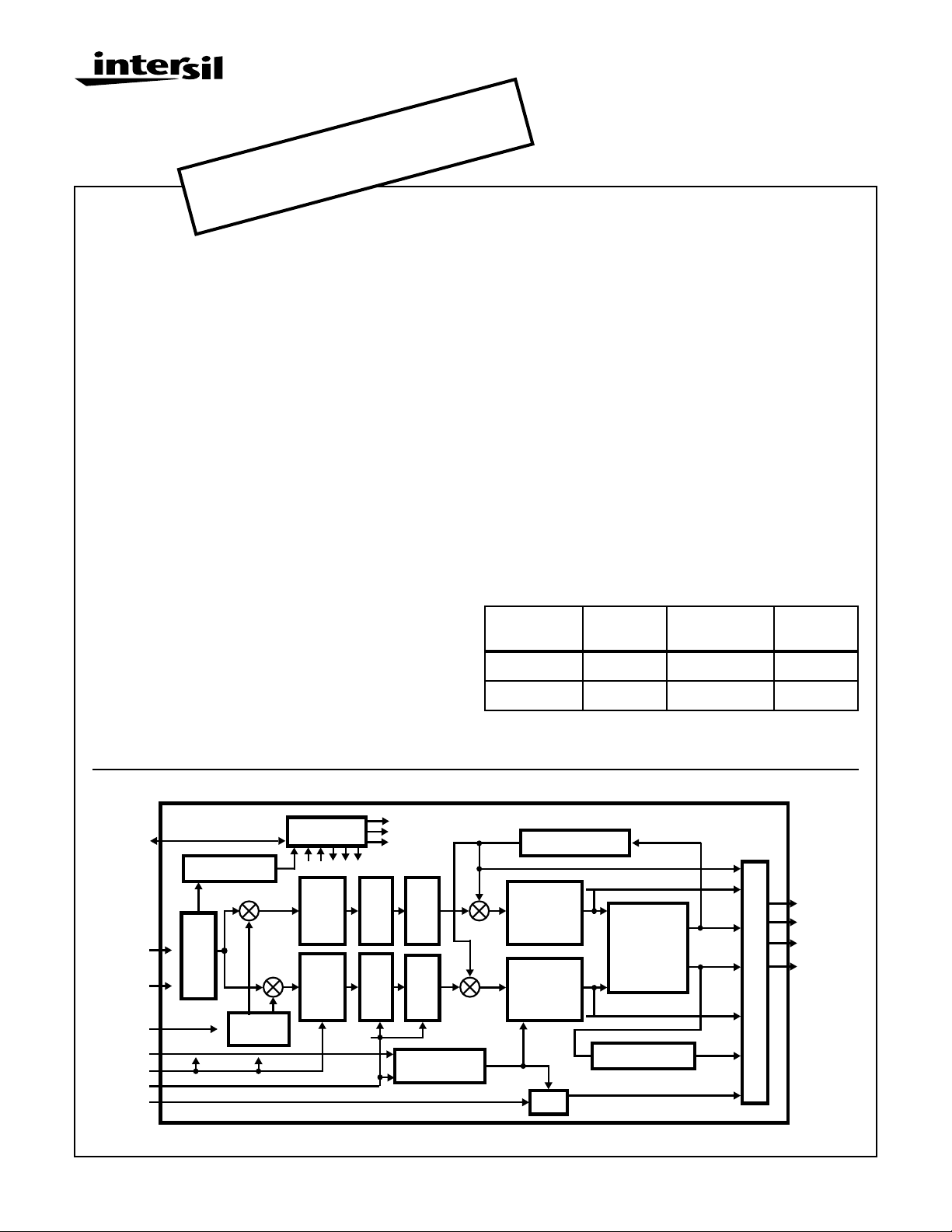
Block Diagram
MICROPROCESSOR
C(7:0)
IN(13:0)
GAIN
ADJ
(2:0)
COF
SOF
CLKIN
PROCCLK
REFCLK
READ/WRITE
LEVEL DETECT
INPUT
SECTION
CARRIER
NCO
CONTROL
TH
5
ORDER
CIC
FILTER
TH
5
ORDER
CIC
FILTER
HALFBAND
HALFBAND
FILTERS
FILTERS
RESAMPLING
255-TAP
255-TAP
FIR FILTER
FIR FILTER
NCO
Programmable Downconverter
Description
The HSP50214A ProgrammableDownconverter converts digitized IF data into filtered baseband data which can be processed by a standard DSP microprocessor. The
Programmable Downconverter (PDC) performs down conversion, decimation, narrowband low pass filtering, gain scaling,
resampling, and Cartesian to Polar coordinate conversion.
The 14-bit sampled IF input is down converted to baseband
by digital mixers and a quadrature NCO, as shown in the
Block Diagram. A decimating (4 to 32) fifth order Cascaded
Integrator-Comb (CIC) filter can be applied to the data
before it is processed by up to 5 decimate-by-2 halfband filters. The halfband filters are followed by a 255-tap programmable FIR filter. The output data from the
programmable FIR filter is scaled by a digital AGC before
being re-sampled in a polyphase FIR filter. The output section can provide seven types of data: Cartesian (I, Q), polar
(R, q), filtered frequency (dq/dt), Timing Error (TE), and
AGC level in either parallel or serial format.
Ordering Information
PART
NUMBER
HSP50214AVC 0 to 70 120 Ld MQFP Q120.28x28
HSP50214AVI -40 to 85 120 Ld MQFP Q120.28x28
AGC LOOP FILTER
POLYPHASE
FIR AND
HALFBAND
FILTERS
POLYPHASE
FIR AND
HALFBAND
FILTERS
∆
TEMP.
RANGE (oC) PACKAGE PKG. NO.
AGC
I OUT
CARTESIAN
TO
POLAR
COORDINATE
CONVERTER
Q OUT
DISCRIMINATOR
TIMING ERROR
MAG.
PHASE
FREQ
SEROUTA
SEROUTB
AOUT(15:0)
BOUT(15:0)
OUTPUT FORMATTER
CAUTION: These devices are sensitive to electrostatic discharge; follow proper IC Handling Procedures.
1-888-INTERSIL or 321-724-7143
| Copyright © Intersil Corporation 1999
1
File Number 4449.1

Pinout
IN11
IN12
IN13
REFCLK
VCCAGCGNSEL
GND
AOUT15
OEAH
HSP50214A
120 LEAD MQFP
TOP VIEW
AOUT10
AOUT11
AOUT12
AOUT13
AOUT14
GND
NC
AOUT8
AOUT9
AOUT6
AOUT7
VCCAOUT5
NC
AOUT3
AOUT4
AOUT1
AOUT2
GND
AOUT0
OEAL
IN10
IN9
IN8
GND
IN7
NC
IN6
IN5
IN4
IN3
IN2
GND
IN1
IN0
V
CC
CLKIN
GND
NC
ENI
GAINADJ2
GAINADJ1
GAINADJ0
COF
COFSYNC
GND
SOF
SOFSYNC
V
CC
SYNCIN1
SYNCIN2
103
102
101
100
114
113
112
111
117
118
119
120
1
2
3
4
5
6
7
8
9
10
11
12
13
14
15
16
17
18
19
20
21
22
23
24
25
26
27
28
29
30
32
31
115
116
333435363738394041424344454647484950515253545556575859
105
104
106
107
108
109
110
95
96
97
98
99
91
92
93
94
60
90
89
88
87
86
85
84
83
82
81
80
79
78
77
76
75
74
73
72
71
70
69
68
67
66
65
64
63
62
61
DATARDY
OEBH
BOUT15
BOUT14
V
CC
NC
BOUT13
BOUT12
BOUT11
BOUT10
BOUT9
BOUT8
GND
GND
PROCCLK
V
CC
MSYNCI
MSYNCO
GND
BOUT7
BOUT6
BOUT5
GND
BOUT4
NC
BOUT3
BOUT2
BOUT1
BOUT0
OEBL
WR
INTRRP
SYNCOUT
RD
GND
C7
C6NCC5
C3C2C1NCC0A2A1
C4
CC
V
A0
GND
SEL2
SEL1
GND
SEL0
SEROUTA
SEROUTB
SEROE
SERCLK
SERSYNC
CC
V
2

HSP50214A
Pin Descriptions
NAME TYPE DESCRIPTION
V
CC
GND - Ground.
CLKIN I Input Clock. This clock should be a multiple of the input sample rate. All input section processing oc-
IN(13:0) I Input Data. The format of the input data may be set to offset binary or 2’s complement. IN13 is the
ENI I Input Enable. Active Low. This pin enables the input to the part in one of two modes, gated or inter-
GAINADJ(2:0) I GAINADJ Input. Adds an offset to the gain via the shifter following the mixer.GAINADJvalueisadded
PROCCLK I Processing Clock. PROCCLK is the clock for all processing functions following the CIC Section. Pro-
AGCGNSEL I AGC Gain Select. This pin selects between two AGC loop gains. This input is setup and held relative
COF I Carrier Offset Frequency Input. This serial input pin is used to load the carrier offset frequency into the
COFSYNC I Carrier Offset FrequencySync. This signal is asserted one CLK before the most significant bit (MSB)
SOF I Re-Sampler Offset Frequency Input. This serial input pin is used to load the offset frequency into the
SOFSYNC I Re-Sampler Offset Frequency Sync. This signal is asserted one CLK before the MSB of the offset
AOUT(15:0) O ParallelOutput Bus A. Two parallel output modes are available on the HSP50214A. The first is called
BOUT(15:0) O ParallelOutput Bus B. Two parallel output modes are available on the HSP50214A. The first is called
- Positive Power Supply Voltage.
curs on the rising edge of CLKIN. The frequency of CLKIN is designated f
MSB (see Control Word 0).
polated (see Control Word 0). In gated mode, one sample is taken per CLKIN when ENI is asserted.
The input sample rate is designated fS, which can be different from f
to the shift code from the microprocessor (µP) interface. The shift code is saturated to a maximum
code of F. The gain is offset by (6dB)(GAINADJ); (000 = 0dB gain adjust; 111 = 42dB gain adjust)
GAINADJ2 is the MSB. See “Using the Input Gain Adjust Control Signals” Section.
cessing is performed on PROCCLK’s rising edge. All output timing is derived from this clock.
NOTE: This clock may be asynchronous to CLKIN.
to PROCCLK. Gain setting 1 is selected when AGCGNSEL = 1.
Carrier NCO (see Serial Interface Section). The offset may be 8, 16, 24, or 32 bits. The setup and hold
times are relative to CLKIN. This input is compatible with the output of the HSP50210 Costas loop [1].
of the offset frequency word (see Serial Interface Section). The setup and hold times are relative to
CLKIN. This input is compatible with the output of the HSP50210 Costas loop [1].
Re-Sampler NCO (see Serial Interface Section). The offset may be 8, 16, 24, or 32 bits. The setup
and hold times are relative to PROCCLK. This input is compatible with the output of the HSP50210
Costas loop [1].
frequency word (see Serial Interface Section). The setup and hold times are relative to PROCCLK.
This input is compatible with the output of the HSP50210 Costas loop [1].
the Direct Output Port, where the source is selected through Control Word 20 (see the Microprocessor Write Section) and comes directly from the Output MUX Section (see Output Control Section).
The most significant byte of AOUT alwaysoutputs the most significant byte of the Parallel Direct Output Port whose data type is selected via µP interface. AOUT15 is the MSB. In this mode, the
AOUT(15:0) bus is updated as soon as data is available. DATARDYis asserted to indicate new data.
The second mode for parallel data is called the Buffer RAM Output Port. The Buffer RAM Output Port
acts like a FIFO for blocks of information called data sets. Within a data set is I, Q, magnitude, phase,
and frequency information; a data type is selected using SEL(2:0). Up to 7 data sets are stored in the
BufferRAMOutputPort.TheLSBytesoftheAOUTandBOUTbussesform the 16bitsforthebuffered
output mode and can be used for buffered mode while the MSBytes are outputting data in the direct
output mode.
the Direct Output Port, where the source is selected through Control Word 20 (see the Microprocessor Write Section) and comes directly from the Output MUX Section (see Output Control Section).
The most significant byte of BOUT always outputs the most significant byte of the Parallel Direct Output Port whose data type is selected via µP interface. BOUT15 is the MSB. In this mode, the
BOUT(15:0) bus is updated as soon as data is available. DATARDYis asserted to indicate new data.
The second mode for parallel data is called the Buffer RAM Output Port. The Buffer RAM Output Port
acts like a FIFO for blocks of information called data sets. Within a data set is I, Q, magnitude, phase,
and frequency information; a particular information is selected using SEL(2:0). Up to 7 data sets is
stored in the BufferRAM Output Port. The least significant byte of BOUT can be used to either output
the least significant byte of the B Parallel Direct Output Port or the least significant byte of the Buffer
RAM Output Port. See Output Section.
CLKIN
When ENI is used.
CLKIN
.
3

HSP50214A
Pin Descriptions (Continued)
NAME TYPE DESCRIPTION
DATARDY O Output Strobe Signal. Active Low. Indicates when new data from the Direct Output Port Section is
available.DATARDY is asserted for one PROCCLK cycle during the first clock cycle that data is available on the parallel out busses. See Output Section.
OEAH I Output enable for the MSByte of the AOUT bus. Active Low.
OEAL I Output enable for the LSByte of the AOUT bus. Active Low.
OEBH I Output enable for the MSByte of the BOUT bus. Active Low.
OEBL I Output enable for the LSByte of the BOUT bus. Active Low.
SEL(2:0) I Select Address is used to choose which information in a data set from the Buffer RAM Output Port is
sent to the least significant bytes of AOUT and BOUT. SEL2 is the MSB.
INTRRP O Interrupt Output. Active Low. This output is asserted for 8 PROCCLK cycles when the Buffer RAM
Output Port is ready for reading.
SEROUTA O Serial Output Bus A Data. I, Q, magnitude, phase, frequency, timing error and AGC information can
be sequenced in programmable order. See Output Section and Microprocessor Write Section.
SEROUTB O Serial Output Bus B Data. Contents may be related to SEROUTA.I, Q, magnitude, phase, frequency,
timing error and AGCinformation can be sequenced in programmable order. See Output Section and
Microprocessor Write Section.
SERCLK O Output Clock for Serial Data Out. Derived from PROCCLK as given by Control Word 20 in the Micro-
processor Write Section.
SERSYNC O Serial Output Sync Signal. Serves as serial data strobes. See Output Section and Microprocessor
Write Section.
SEROE I Serial Output Enable. When high, the SEROUTA, SEROUTB, SERCLK, and SERSYNC signals are
set to a high impedance.
C(7:0) I/O Processor Interface Data Bus. See Microprocessor Write Section. C7 is the MSB.
A(2:0) I Processor Interface Address Bus. See Microprocessor Write Section. A2 is the MSB.
WR I Processor Interface Write Strobe. C(7:0) is written to Control Words selected by A(2:0) in the Pro-
grammable Down Converter on the rising edge of this signal. See Microprocessor Write Section.
RD I Processor Interface Read Strobe. C(7:0) is read from output or status locations selected by A(2:0)
in the Programmable Down Converter on the falling edge of this signal. See Microprocessor Read
Section.
REFCLK I Reference Clock. Used as an input clock for the timing error detector. The timing error is computed
relative to REFCLK. REFCLK frequency must be less than or equal to PROCCLK/2.
MSYNCO O Multiple Chip Sync Output. Provided for synchronizing multiple parts when CLKINand PROCCLK are
asynchronous. MSYNCO is the synchronization signal between the input section operating under
CLKIN and the back end processing operating under PROCCLK. This output sync signal from one
part is connected to the MSYNCI signal of all the HSP50214As.
MSYNCI I Multiple Chip Sync Input. The MSYNCI pin of all the parts should be tied to the MSYNCO of one part.
NOTE: MSYNCI must be connected to an MSYNCO signal for operation.
SYNCIN1 I CICDecimation/CarrierNCOUpdateSync.CanbeusedtosynchronizetheCICSection,carrierNCO
update, or both. See the Multiple Chip Synchronization Section and Control Word 0 in the Micropro-
cessor Write Section. Active High.
SYNCIN2 I FIR/Timing NCO Update/AGC Gain Update Sync. Can be used to synchronize the FIR, Timing NCO
update, AGC gain update, or any combination of the above. See the Multiple Chip Synchronization
Section and Control Words 7, 8, and 10 in the Microprocessor Write Section. Active High.
SYNCOUT O StrobeOutput.Thissynchronization signal is generated by the µP interfaceforsynchronizingmultiple
parts. Can be generated by PROCLK or CLKIN (see Control Word 0 and Control Word 24 in the Mi-
croprocessor Write Section). Active High.
4

AGCGNSEL
TO OUTPUT FORMATTER
PROCCLK
GAINADJ(2:0)
ENI
IN(13:0)
DETECT
µPROCESSOR
INTERFACE
CLKIN
INPUT
LEVEL
TO
SECTION
MIXER
5TH ORDER
CIC
DECIMATE
FROM 4-32
0 TO 5 HALFBAND FILTER;
DECIMATION UP TO 32
AND MICROPROCESSOR
INTERFACE
= 1;
(C
O
= 0)
C
n
255-TAP
PROGRAMMABLE
FIR FILTER
(DECIMATE UP TO 16)
5
= 1;
COF
COFSYNC
SOF
SOFSYNC
REFCLK
RD
WR
A(2:0)
C(7:0)
COS
SIN
NCO
(CARRIER TRACKING)
MICROPROCESSOR
READ/WRITE
CONTROL
SECTION
OUTPUT SECTION
DISCRIMINATOR SECTION
INPUT SECTION
LEVEL DETECT SECTION
SYNCHRONIZATION SECTION
CARRIER NCO SECTIONS
CIC, HALFBAND FILTER, AND FIR SECTIONS
DIGITAL AGC SECTION
RE-SAMPLER/INTERPOLATION HALFBAND SECTION
TIMING NCO
(C
O
= 0)
C
n
(SYMBOL TRACKING)
AGCOUT
SHIFT
AGC
SHIFT
NCO
A
LIMIT
FILTER
POLYPHASE
RE-SAMPLER
FILTER
POLYPHASE
DIFFERENCE
PROCCLK
INTERPOLATE
BY 2/4
HALFBAND
FILTERS
DISCRIMINATOR
CLKIN
LOOP
FILTER
CARTESIAN
POLAR
I
atan
Q
dθ
63-TAP
PROGRAMMABLE
FIR FILTER
td
TIMING ERROR
A
SYNCHRONIZATION
CIRCUITRY
BACK END
SYNCHRONIZATION
CIRCUITRY
FRONT END
SYNCHRONIZATION
CIRCUITRY
ERROR
DETECT
TO
I2Q2+
Q
----
AGCOUT
CHIP
DATARDY
INTRRP
AOUT(15:0)
BOUT(15:0)
I
OUTPUT FORMATTER
OEAH
OEAL
OEBH
OEBL
INTRRP
SEL(2:0)
SEROUTA
SEROUTB
SERCLK
SERSYNC
SEROE
MSYNCI
SYNCOUT
MSYNCO
SYNCIN2
SYNCIN1
HSP50214A
FIGURE 1. FUNCTIONAL BLOCK DIAGRAM OF THE HSP50214A PROGRAMMABLE DOWNCONVERTER
HSP50214A
Functional Description
The HSP50214A Programmable Downconverter (PDC) is an
agile digital tuner designed to meet the requirements of a
wide variety of communications industry standards. The
PDC contains the processing functions needed to convert
sampled IF signals to baseband digital samples. These functions include LO generation/mixing, decimation filtering, programmable FIR shaping/bandlimiting filtering, resampling,
Automatic Gain Control (AGC), frequency discrimination and
detection as well as multi-chip synchronization. The
HSP50214A interfaces directly with a DSP microprocessor
to pass baseband and status data.
A top level functional block diagram of the HSP50214A is
shown in Figure 1. The diagram shows the major blocks and
multiplexers used to reconfigure the data path for various
architectures. The HSP50214A can be broken into 13 sections: Synchronization, Input, Input Level Detector, Carrier
Mixer/Numerically Control Oscillator (NCO), CIC Decimating
Filter, Halfband Decimating Filter, 255-Tap Programmable
FIR Filter, Automatic Gain Control (AGC), Re-sampler/Halfband Filter, Timing NCO, Cartesian to Polar Converter, Discriminator, and Output Sections. All of these sections are
configured through a microprocessor interface.
The HSP50214A has three clock inputs; two are required and
one is optional. The input level detector, carrier NCO, and CIC
decimating filter sections operate on the rising edge of the
input clock, CLKIN. The halfband filter, programmable FIR filter, AGC, Re-Sampler/Halfband filters, timing NCO, discriminator, and output sections operate on the rising edge of
PROCCLK. The third clock, REFCLK, is used to generate timing error information.
NOTE: All of the clocks may be asynchronous.
PDC Applications Overview
This section highlights the motivation behind the key programmable features from a communications system level perspective. These motivations will be defined in terms of ability to
provide DSP processing capability for specific modulation formats and communication applications. The versatility of the
Programmable Downconverter can be intimidating because of
the many Control Words required for chip configuration. This
section provides system level insight to help allay reservations
about this versatile DSP product. It should help the designer
capitalize on the greatest feature of the PDC - VERSATILITY
THROUGH PROGRAMMABILITY. It is this feature, when fully
understood, that brings the greatest return on design investment by offering a single receiver design that can process the
many wav ef orms required in the communications marketplace.
FDM Based Standards and Applications
Table 1 provides an overview of some common frequency
division multiplex (FDM) base station applications to which the
PDC can be applied. The PDC provides excellent selectivity
for frequency division multiple access (FDMA) signals. This
high selectivity is achiev ed with 0.012Hz resolution frequency
control of the NCO and the sharp filter responses capable
with a 255-tap, 22-bit coefficient FIR filter. The 16-bit resolution out of the Cartesian to Polar Coordinate Converter are
routed to the frequency detector, which is followed by a 63tap, 22-bit coefficient FIR filter structure for facilitating FM and
FSK detection. The 14-bit input resolution is the smallest bit
resolution found throughout the conversion and filtering sections, providing excellent dynamic range in the DSP processing. A unique input gain scaler adds an additional 42dB of
range to the input level variation, to compensate for changes
in the analog RF front end receive equipment. Synchronization circuitry allows precise timing control of the base station
reconfiguration for all receive channels simultaneously. Portions of this table were corroborated with reference [2].
TABLE 1. CELLULAR PHONE BASE STATION APPLICATIONS
USING FDMA
STANDARD
RX BAND
(MHz)
CHANNEL
BW (kHz)
# TRAFFIC
CHANNELS
VOICE
MODULA-
TION
PEAK
DEVIA TION
(kHz)
CONTROL
MODULA-
TION
PEAK
DEVIA TION
(kHz)
CONTROL
CHANNEL
RA TE
(Kbps)
AMPS
(IS-91)
824-849 925-940 453-458
FSK FSK FSK FSK FSK
MCS-L1
MCS-L2
30 25.0
12.5
832 600
1200
FM FM FM FM FM
12 5 5 4 9.5
8 4.5 3.5 2.5 6.4
10 0.3 1.2 5.3 8
NMT-400
NMT-900 C450
451-456 871-904
890-915
25
12.5
200
1999
20.0
10.0
222
444
ETACS
NTACS
915-925
25.0
12.5
1240
800
TDM Based Standards and Applications
Table 2 provides an overview of some common Time Division Multiplexed (TDM) base station applications to which
the PDC can be applied. For time division multiple access
(TDMA) applications, such as North American TDMA
(IS136), where 30kHz is the received band of interest for the
PCS basestation, the PDC offers 0.012Hz frequency resolution in downconversion in addition to α = 0.35 matched (programmable) filtering capability. The π/4 DPSK modulation
can be processed using the PDC Cartesian to Polar coordinate converter and dφ/dt detector circuitry or by processing
the I/Q samples in the DSP µP. The PDC provides the ability
to change the received signal gain and frequency, synchronous with burst timing. The synchronous gain adjustment
allows the user to measure the power of the signal at the A/D
at the end of a burst, and synchronously reload that same
gain value at the arrival of the next user burst.
For applications other than cellular phones (where the preambles are not changed), the PDC frequency discriminator
output can be used to obtain correlation on the preamble
pattern to aid in burst acquisition.
6

HSP50214A
TABLE 2. CELLULAR BASESTATION APPLICATIONS USING
TDMA
STANDARD GSM PCN IS-54
TYPE Cellular Cellular Cellular
BASESTATION RX
BAND (MHz)
CHANNEL BW (kHz) 200 200 30
# TRAFFIC CHANNELS 8163
VOICE MODULATION GMSK GMSK π/4
CHANNEL RATE (Kbps) 270.8 270.8 48.6
CONTROL
MODULATION
CHANNEL RATE (Kbps) 270.8 270.8 48.6
935-960 1805-1880 824-849
DQPSK
GMSK GMSK π/4
DQPSK
Several applications are combinations of frequency and time
domain multiple access schemes. For example, GSM is a
TDMA signal that is frequency hopped. The individual channels contain Gaussian MSK modulated signals. The PDC
again offers the 0.012Hz tuning resolution for de-hopping the
received signal. The combination of halfband and 256-tap
programmable, 22-bit coefficient FIR filters readily performs
the necessary matched filtering for demodulation and optimum detection of the GMSK signals.
CDMA Based Standards and Applications
For Code Division Multiple Access (CDMA) type signals, the
PDC offers the ability to have a single wideband RF front
end, from which it can select a single spread channel of
interest. The synchronization circuitry provides for easy control of multiple PDC for applications where multiple received
signals are required, such as base-stations.
In IS-95 CDMA, the receive signal bandwidth is approximately 1.2288MHz wide with many spread spectrum channel in the band. The PDC supplies the downconversion and
filtering required to receive a single RF channel in the presence of strong adjacent interference. Multiple PDC’s would
be sourced from a single receive RF chain, each processing
a different receive frequency channel. The despreader would
usually follow the PDC. In some very specific applications,
with short, fixed codes, the filtering and despreading may be
possible with innovative use of the programmable, 22-bit
coefficient FIR filter. The PDC offers 0.012Hz resolution on
tuning to the desired receive channel and excellent rejection
of the portions of the band not being processed, via the halfband and 255-tap programmable, 22-bit coefficient FIR filter.
Traditional Modulation Formats
AM, ASK, FM and FSK
The PDC has the capability to fully demodulate AM and FM
modulated waveforms.The PDC outputs 15 bits of amplitude or
16 bits of frequency for these modulation formats. The FM discriminator has a 63-tap programmable, 22-bit coefficient FIR filter for additional signal conditioning of the FM signal. Digital
versions of these formats, ASK and FSK are also readily pro-
cessed using the PDC. Just as in the AM modulated case, ASK
signals will use 15-bit magnitude output of the Cartesian to
Polar Coordinate converter. Multi-tone FSK can be processed
several ways. The frequency information out of the discriminator can be used to identify the received tone, or the filter can be
used to identify and power detect a specific tone of the received
signal. AMPS is an example of an FM application.
PM and PSK
The PDC provides the downconversion, demodulation,
matched filtering and coordinate conversion required for
demodulation of PM and PSK modulated waveforms. These
modulation formats will require external carrier and symbol
timing recovery loop filters to complete the receiver design.
The PDC was designed to interface with the HSP50210 Digital Costas Loop to implement the carrier phase and symbol
timing recovery loop filters (for continuous PSK signals - not
burst).
Digital modulation formats that combine amplitude and
phase for symbol mapping, such as m-ary QAM, can also be
downconverted, demodulated, and matched filtered. The
received symbol information is provided with 16 bits of resolution in either Cartesian or Polar coordinates to facilitate
remapping into bits and to recover the carrier phase. External Symbol mapping and Carrier Recovery Loop Filtering is
required for this waveform.
Resampling and Interpolation Filters
Two key features of the resampling FIR filter are that the resampler filter allows the output sample rate to be programmed
with millihertz resolution and that the output sample rate can
be phase locked to an independent separate clock. The resampler frees the front end sampling clocks from having to be
synchronous or integrally related in rate to the baseband
output. The asynchronous relationship between front end
and back end clocks is critical in applications where ISDN
interfaces drive the baseband interfaces, but the channel
sample rates are not related in any way. The interpolation
halfband filters can increase the rate of the output when narrow frequency bands are being processed. The increase in
output rate allows maximum use of the programmable FIR
while preserving time resolution in the baseband data.
14-Bit Input and Processing Resolution
The PDC maintains a minimum of 14 bits of processing resolution through to the output, providing over 84dB of dynamic
range. The 18 bits of resolution on the internal references
provide a spurious floor that is better than 98dBc. Furthermore, the PDC provides up to 42dB of gain scaling to compensate for any change in gain in the RF front end as well as
up to 96dB of gain in the internal PDC AGC. This gain maximizes the output resolution for small signals and compensates for changes in the RF front end gain, to handle
changes in the incoming signal.
7

HSP50214A
Summary
The greatest feature of the PDC is its ability to be reconfigured to process many common standards in the communications industry. Thus, a single hardware element can receive
and process a wide variety of signals from PCS to traditional
cellular, from wireless local loop to SATCOM. The high resolution frequency tuning and narrowband filtering are instrumental in almost all of the applications.
Multiple Chip Synchronization
Multiple PDCs are synchronized using a MASTER/SLAVE
configuration. One part is responsible for synchronizing the
front end internal circuitry using CLKIN while another part is
responsible for synchronizing the backend internal circuitry
using PROCCLK.
The PDC is synchronized with other PDCs using five control
lines: SYNCOUT, SYNCIN1, SYNCIN2, MSYNCO, and
MSYNCI. Figure 2 shows the interconnection of these five
signals for multiple chip synchronization where different
sources are used for CLKIN and PPOCCLK.
PDC A is the Master sync through MSO.
PDC B configures the CLKIN sync through SYNCIN1.
PDC A configures the PROCCLK sync through SYNCIN2.
AB
HSP50214A
MSYNCO
MSYNCI
(MASTER
SYNCIN2)
SYNCOUT
SYNCIN2
SYNCIN1
FIGURE 2. SYNCHRONIZATION CIRCUIT
SYNCOUT for PDC B should be set to be synchronous with
CLKIN (Control Word 0, Bit 3 = 0. See the Microprocessor
Write Section). SYNCOUT for PDC B is tied to the SYNCIN1
of all the PDCs. The SYNCIN1 can be programmed so that
the carrier NCO and/or the 5th order CIC filter of all PDCs can
be synchronously loaded/updated using SYNCIN1. See Control Word 0, Bits 19 and 20 in the Microprocessor Write Section for details.
SYNCOUT for one of the PDC’s other than PDC B, should
be set for PROCCLK (bit 3 = 1 in Control Word 0). This output signal is tied to the SYNCIN2 of all PDCs. The SYNCIN2
can be programmed so that the AGC updates its accumulator with the contents in the master registers (Control Word 8,
Bit 29 in the Microprocessor Write Section). SYNCIN2 is
also used to load or reset the timing NCO using bit 5, Control
Word 11. The halfband and FIR filters can be reset on
HSP50214A
MSYNCO
MSYNCI
SYNCOUT
SYNCIN2
SYNCIN1
ALL OTHER SYNCIN1
ALL OTHER SYNCIN2
ALL OTHER MSI
(MASTER
SYNCIN1)
SYNCIN2 using Control Word 7, Bit 21. The MSYNCO of
one of the PDCs is then used to drive the MSYNCI of all the
PDCs (including its own).
For application configurations where CLKIN and PROCCLK
have the same source, SYNCIN1 and SYNCIN2 can be tied
together.However, if different enabling is desired for the front
end and backend processing of the PDC’s, these signals can
still be controlled independently.
In the HSP50214A, the Control Word 25 reset signal has
been extended so that the front end reset is 10 CLKIN periods wide and the back end reset is 10 PROCCLK periods
wide. This guarantees that no enables will be caught in the
pipelines. In addition, the SYNCIN1 internal reset signal,
which is enabled by setting Control Word 7, Bit 21 = 1, has
been extended to 10 cycles.
In summary, SYNCIN1 is used to update carrier phase offset, update carrier center frequency, reset CIC decimation
counters and reset the carrier NCO (clear the feedback in
the NCO). SYNCIN2 is used to reset the HB filter, FIR filter,
re-sampler/HB state machines and the output FIFO, load a
new gain into the AGC and load a new re-sampler NCO center frequency and phase offset.
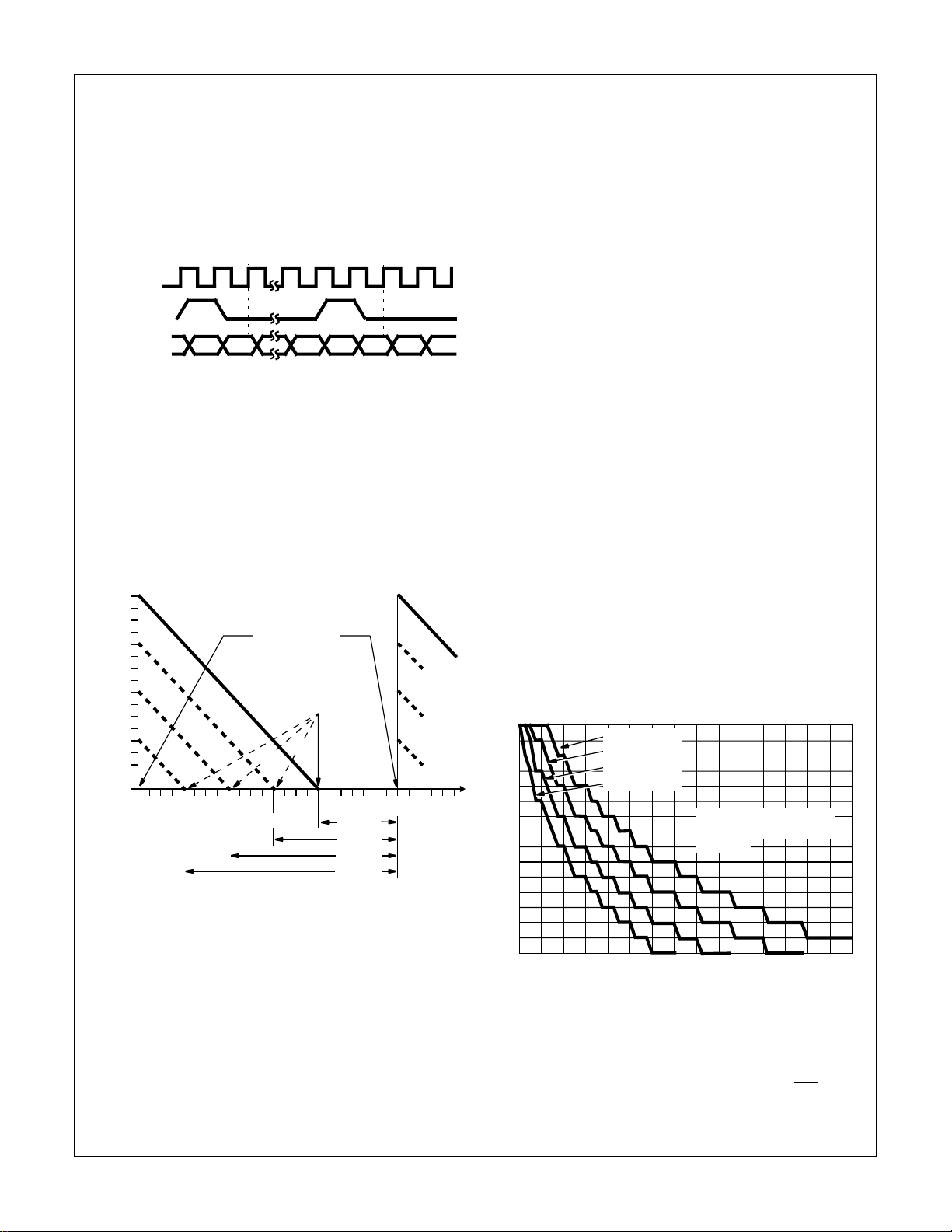
Input Section
The block diagram of the input controller is provided in Figure 3. The input can support offset binary or two’s complement data and can be operated in gated or interpolated
mode (see Control Word 0 from the Microprocessor Write
Section). The gated mode takes one sample per clock when
the input enable (ENI) is asserted. The gated mode allows
the user to synchronize a low speed sampling clock to a high
speed CLKIN.
The interpolated mode allows the user to input data at a low
sample rate and to zero-stuff the data prior to filtering. This
zero stuffing effectively interpolates the input signal up to the
rate of the input clock (CLKIN). This interpolated mode
allows the part to be used at rates where the sampling frequency is above the maximum input rate range of the halfband filter section, and where the desired output bandwidth
is too wide to use a Cascaded Integrator Comb (CIC) filter
without significantly reducing the dynamic range. See Figures 4-7 for an interpolated input example, detailing the
associated spectral results.
Interpolation Example:
The specifications for the interpolated input example are:
Input Sample Rate = 5 MSPS
PROCCLK = 28MHz
Interpolate by 8, Decimate by 10
Desired 85dB dynamic range output bandwidth = 500kHz
Input Level Detector
The Input Level Detector Section measures the average
magnitude error at the PDC input for the microprocessor by
comparing the input level against a programmable threshold and then integrating the result. It is intended to provide
8

HSP50214A
a gain error for use in an AGC loop with either the RF/IF or
A/D converter stages (see Figure 8). The AGC loop
includes Input Level Detector, the microprocessor and an
external gain control amplifier (or attenuator). The input
samples are rectified and added to a threshold programmed via the microprocessor interface, as shown in
Figure 9. The bit weighting of the data path through the
input threshold detector is shown in Figure 10. The threshold is a signed number, so it should be set to the inverse of
the desired input level. The threshold can be set to zero if
the average input level is desired instead of the error. The
sum of the threshold and the absolute value of the input is
accumulated in a 32-bit accumulator. The accumulator can
INPUT LEVEL DETECTOR †
STATUS (0) †
LEVEL
DETECT
14
IN(13:0)
FORMAT
INPUT
†
GAINADJ(2:0)
REG
INPUT FORMAT
REG
14
NCO††
EN
handle up to 2
18
samples without overflow. The integration
time is controlled by an 18-bit counter. The integration
counter preload (ICPrel) is programmed via the microprocessor interface through Control Word 1. Only the upper 16
bits are programmable. The 2 LSBs are always zero. Control Word 1, Bits 29-14 are programmed to:
ICPrel N()41+⁄=
where N is the desired integration period, defined as the
number of input samples to be integrated. N must be a multi-
ple of 4: [0, 4, 8, 12, 16 .... , 2
INPUT_THRESH †
INTG_MODE †
INTG_INTEVAL †
REGREG
18
18
DELAY 3
SHIFT
4
LIMIT
3
∑
BYPASS †
CIC
18
].
MUX
(EQ. 1)
ENI
CONTROL WORD 0
CONTROL WORD 1
CLKIN
INTERP †
CONTROL
LOGIC
DELAY 3
INPUT_MODE †
INPUT_FMT †
INPUT_THRESH†
INTG_MODE†
INTG_INTEVAL†
FIGURE 3. BLOCK DIAGRAM OF THE INPUT SECTION
5MHz
BYPASS
CIC
FILTER
MIN. R = 4
PROCCLK = 28MHz
HB/FIR FILTER
MUX
MAX. fS = 4MHz
(EXCEEDED IN
BYPASS PATH)
500kHz = 85dB
BANDWIDTH
(NOT ACHIEVED
WITH CIC FILTER
PATH)
Without Interpolation, the CIC bypass path exceeds the HB/FIR filter
input sample rate and the CIC filter path will not yield the desired 85dB
dynamic range band width of 500kHz.
FIGURE 4. STATEMENT OF THE PROBLEM
4
† Controlled via microprocessor interface.
††See NCO Section for more details.
↑8 (0 STUFF) = 40MHz
5MHz
CIC FILTER
R = ↓10
FIGURE 5. BLOCK DIAGRAM OF THE INTERPOLATION
APPROACH
4MHz
HB/FIR FILTER
500kHz = 85dB
BANDWIDTH
9

HSP50214A
f
S
5MHz 10MHz 15MHz 20MHz 25MHz 30MHz 35MHz 40MHz 45MHz 50MHz
5MHz 10MHz 15MHz 20MHz 25MHz 30MHz 35MHz 40MHz
2f
3f
S
S
THE INPUT DATA SPECTRUM SAMPLED AT RATE R = fs
4f
f’S/2f’S/4f’S/8 3f’S/8 5f’S/8 7f’S/83f’S/4
5f
S
S
6f
S
7f
8f
S
S
f’
S
9f
10f
S
S
FIGURE 6. INTERPOLATION SPECTRUM: INTERPOLATE BY 8 THE INPUT DATA WITH ZERO STUFFING; SAMPLE ATRATE R = f’
8MHz 12MHz 16MHz 20MHz 24MHz 28MHz 32MHz 36MHz 40MHz
4MHz
DECIMATE BY 10 AND CIC FILTER; SAMPLE AT RATE R = f’S/10
85dB DYNAMIC RANGE BANDWIDTH
4MHz2MHz1MHz 3MHz
CIC FILTER
FREQUENCY
RESPONSE
CIC FILTER ALIAS PROFILE
O.5MHz
FIGURE 7. ALIAS PROFILE AND THE 85dB DYNAMIC RANGE BANDWIDTH
µPROC
DAC
INPUT LEVEL
DETECTOR (24-BIT
ERROR VALUE)
S
THRESH
PDC
INPUT
IF
GCA
A/D
FIGURE 8. PROCESSOR BASED EXTERNAL IF AGC
10

HSP50214A
INPUT
IN(13:0)
INPUT_THRESHOLD †
INTEGRATION_INTERVAL†
INTEGRATION_MODE†
GATING
LOGIC
START †
CLKIN
† Controlled via microprocessor interface.
ACCUMULATOR
|X|
R
E
G
16
COUNTER
CONTINUOUS SINGLE
+ +
CLKIN
“0”
FIGURE 9.
R
E
G
ADDR(2:0)
24
M
U
X
TO
µPROC
8
32
R
E
G
11

FS
-6dB
-12dB
-18dB
-24dB
-30dB
-36dB
-42dB
-48dB
-54dB
-60dB
-66dB
-72dB
-78dB
A/D
0
2
-1
2
-2
2
-3
2
-4
2
-5
2
-6
2
-7
2
-8
2
-9
2
-10
2
-11
2
-12
2
-13
2
OUTPUT
0
2
-1
2
-2
2
-3
2
-4
2
-5
2
-6
2
-7
2
-8
2
-9
2
-10
2
-11
2
-12
2
-13
2
INPUT
MAGNITUDE
0
-1
2
-2
2
-3
2
-4
2
-5
2
-6
2
-7
2
-8
2
-9
2
-10
2
-11
2
-12
2
-13
2
THESHOLD
0
-2
-1
2
-2
2
-3
2
-4
2
-5
2
-6
2
-7
2
-8
2
-9
2
-10
2
-11
2
-12
2
-13
2
HSP50214A
of the accumulator are transferred to a holding register for reading by the microprocessor. Note that it is not the restarting of
the counter (by writing to Control Word 2) that latches the current value, but the end of the integration count. When the accumulator results are latched, a bit is set in the Status Register to
notify the processor. Reading the most significant byte of the 23
READ CODE A(2:0)
ACCUMULATOR
18
2
17
2
16
2
15
2
14
2
13
2
12
2
11
2
10
2
9
2
8
2
7
2
6
2
5
2
4
2
3
2
2
2
1
2
0
2
-1
2
-2
2
-3
2
-4
2
-5
2
-6
2
-7
2
-8
2
-9
2
-10
2
-11
2
-12
2
-13
2
PORTS
µPROC READ
0
18
2
17
2
16
2
15
2
14
2
13
2
12
2
11
2
10
2
9
2
8
2
7
2
6
2
5
2
4
2
3
2
2
2
1
2
0
2
-1
2
-2
2
-3
2
-4
2
bits clears the status bit. See the Microprocessor Read Section.
Figure 10 illustrates a typical AGC detection process.
Typically, the average input error is read from the Input Level
Detector port for use in AGC Applications. By setting the
threshold to 0, however,the average value of the input signal
can be read directly. The calculation is:
dBFS
RMS
20() 1.111()level()N()16()()⁄[]log=
where “level” is the 24-bit value read from the 3 level Detector Registers and “N” is the number of samples to be integrated. Note that to get the RMS value of a sinusoid, multiply
the average value of the rectified sinusoid by 1.111. For a full
scale input sinusoid, this yields an RMS value of approximately 3 dBFS.
NOTE: 1.111 scales the rectified sinusoid average (2/π) to 1/√2
.
A) INPUT SIGNAL
000 010001
AMPLITUDE
C) THRESHOLD
B) RECTIFIED SIGNAL
AMPLITUDE
D) ACCUMULATOR INPUTS
(EQ. 2)
FIGURE 10. INPUT THRESHOLD DETECTOR BIT WEIGHTING
The integration period counter can be set up to run continuously or to count down and stop. Continuous integration
counter operation lets the counter run, with sampling occurring
every time the counter reaches zero. Because the processor
samples the detector read port asynchronous to the CLKIN,
data can be missed unless the status bit is monitored by the
processor to ensure that a sample is taken for every integration
count down sequence.
Additionally, in the HSP50214A, the ability to align the
start/restart of the input level detector integration period with an
external event is provided. This allows the sync signals, which
are synchronized to external events , to be used to align all of
the gain adjustments or measurements. If Control Word 27, Bit
17 is set to a logic one, the SYNCIN1 signal will cause the input
level detector to start/restart its integration period. If Control
Word 27, Bit 17 is set to a logic zero, control of the start/restart
of the input level detector integration period does not respond to
SYNCIN1.
In the count down and stop mode, the microprocessor read
commands can be synchronized to system events,such as the
start of a burst for a TDMA application. The integration counter
can be started at any time by writing to Control Word 2. At the
end of the integration period (counter = 0000), the upper 23 bits
AMPLITUDE
E) DETECTOR OUTPUT
AMPLITUDE
AMPLITUDE
F) CLOSED LOOP STEADY STATE
(CONSTANT INPUT)
AMPLITUDE
FIGURE 11. SIGNAL PROCESSING WITHIN LEVEL DETECTOR
In the HSP50214A, the polarity of the two LSB’s of the integration period pre-load is selectable. If Control Word 27, Bit
23 is set to a logic one, the two LSB’s of the integration
period preload are set to logic ones. This allows a power of
two to be set for the integration period, for easy normalization in the processor. If Control Word 27, Bit 23 is set to a
logic zero, then the two LSB’s of the integration period preload are set to zeros as in the HSP50214.
Carrier Synthesizer/Mixer
The Carrier Synthesizer/Mixer Section of the HSP50214A is
shown in Figure 12. The NCO has a 32-bit phase accumulator, a 10-bit phase offset adder, and a sine/cosine ROM.
12

HSP50214A
The frequency of the NCO is the sum of a center frequency
Control Word, loaded via the microprocessor interface (Control Word 3, Bits 0 to 31), and an offset frequency ,loaded serially via the COF and COFSYNC pins. The offset frequency
can be zeroed in Control Word 0, Bit 1. Both frequency control
terms are 32 bits and the addition is modulo 232. The output
frequency of the NCO is computed as:
fCfS* N 232()⁄ ,=
(EQ. 3)
or in terms of the programmed value:
NINTf
C
232fS⁄×[]
HEX
,=
(EQ. 3A)
where N is the 32-bit sum of the center and offset frequency
terms, fC is the frequency of the carrier NCO sinusoids, f
S
the input sampling frequency, and INT is the integer of the
computation. See the Microprocessor Write Section on
instructions for writing Control Word 3.
TO MIXERS
PHASE
ACCUMULATOR
ENI
18 18
REG
REG
SIN/COS
ROM
18
+
REG
SINCOS
CARRIER
PHASE
†
STROBE
R
R
10
E
G
MUX
CARRIER
E
PHASE
G
0
R
E
G
OFFSET
†
CLEAR
PHASE
ACCUM
†
+
COF
ENABLE†
COFSYNC
COF
SYNCIN1
MUX
32
COF
REG
SYNC REG
SHIFT REG
SYNC
CIRCUITRY
32
0
CF
REG
CARRIER
FREQUENCY
CARRIER
FREQUENCY
STROBE
†
f
C
†
CARRIER
LOAD ON
UPDATE
† Controlled via microprocessor interface.
FIGURE 12. BLOCK DIAGRAM OF NCO SECTION
For example, if N is 3267 (decimal), and f
is 65MHz, then fC
S
is 49.44Hz. If received data is modulated at a carrier frequency of 10MHz, then the synthesizer/mixer should be programmed for N = 27627627 (he x) or D89D89B9 (hex).
Because the input enable, ENI, controls the operation of the
phase accumulator, the NCO output frequency is computed
relative to the input sample rate, f
, not to f
S
CLKIN
. The frequency control, N, is interpreted as two’s complement
because the output of the NCO is quadrature. Negative frequency L.O.s select the upper sideband; positive frequency
L.O.s select the lower sideband. The range of the NCO is fS/2 to + fS/2. The frequency resolution of the NCO is fS/(232)
or approximately 0.015Hz when CLKIN is 65 MSPS and ENI
is tied low .
The phase of the Carrier NCO can be shifted by adding a 10bit phase offset to the MSB’s (modulo 360o) of the output of
the phase accumulator. This phase offset control has a resolution of 0.35o and can be interpreted as two’s complement
from -180o to 180o (-p to p) or as binary from 0 to 360o (0 to
2p). The phase offset is given by:
φ
OFF
2π PO 210⁄()× 291–()PO 291–()<<–();=
or, in terms of the parameter to be programmed:
PO INT 210φ
is
()2π⁄]
OFF
HEX
π– φ
OFF
π<<();[=
where PO is the 10-bit two’s complement value loaded into the
Phase Offset Register (Control Word 4, Bits 9-0). For example,
a value of 32 (decimal) loaded into the Phase Offset Register
would produce a phase offset of 11.25o and a value of -512
would produce an offset of 180o. The phase offset is loaded via
the microprocessor interface. See the Microprocessor Write
Section on instructions for writing Control Word 4.
The most significant 18 bits from the phase adder are used as
the address a sin/cos lookup table. This lookup table maps
phase into sinusoidal amplitude. The sine and cosine values
have 18 bits of amplitude resolution. The spurious components in the sine/cosine generation are at least -98dBc. The
sine and cosine samples are routed to the mixer section
where they are multiplied with the input samples to translate
the signal of interest to baseband.
The mixer multiplies the 14-bit input by the 18-bit quadrature
sinusoids. The mixer equations are:
I
OUTIIN
Q
OUTIIN
ωc()cos×=
ωc()sin×=
The mixer output is rounded symmetrically to 15 bits.
To allow the frequency and phase of multiple parts to be
updated synchronously, two sets of registers are used for
latching the center frequency and phase offset words. The offset phase and center frequency Control Words are first
†
loaded into holding registers. The contents of the holding registers are transferred to active registers in one of two ways.
The first technique involves writing to a specific Control Word
Address. A processor write to Control Word 5, transfers the
center frequency value to the active register while a processor
write to Control Word 6 transfers the phase offset value to the
active register .
The second technique, designed for synchronizing updates to
multiple parts, uses the SYNCIN1 pin to update the active
registers. When Control Word 1, Bit 20 is set to 1, the
SYNCIN1 pin causes both the center frequency and Phase
Offset Holding Registers to be transferred to active registers.
Additionally, when Control Word 0, Bit 0 is set to 1, the feedback in the phase accumulator is zeroed when the transfer
from the holding to active register occurs. This feature provides synchronization of the phase accumulator starting
phase of multiple parts. It can also be used to reset the phase
of the NCO synchronous with a specific event.
(EQ. 4)
(EQ. 4A)
(EQ. 5)
(EQ. 5A)
13
HSP50214A
The carrier offset frequency is loaded using the COF and
COFSYNC pins. Figure 13 details the timing relationship
between COF, COFSYNC and CLKIN. The offset frequency
word can be zeroed if it is not needed. Similarly, the
Sample Offset Frequency Register controlling the ReSampler NCO is loaded via the SOF and SOFSYNC pins.
The procedure for loading data through the two pin NCO
interfaces is identical except that the timing of SOF and
SOFSYNC is relative to PROCCLK.
CLKIN
COFSYNC/
SOFSYNC
COF/
SOF
OTE: Data must be loaded MSB first.
IGURE 13. SERIAL INPUT TIMING FOR COF AND SOF INPUTS
MSB
LSB
MSB
Each serial word has a programmable word width of either 8,
16, 24, or 32 bits (See Control Word 0, Bits 4 and 5, for the
Carrier NCO programming and Control Word 11, Bits 3 and
4, for Timing NCO programming). On the rising edge of the
clock, data on COF or SOF is clocked into an input shift register. The beginning of a serial word is designated by asserting either COFSYNC or SOFSYNC “high” one CLK period
prior to the first data bit.
32†
30
28
26
24
22
20
18
16
14
12
10
8
SHIFT COUNTER VALUE
†
†
†
6
4
2
0
ASSERTION OF
COFSYNC, SOFSYNC
DATA TRANSFERRED
TO HOLDING REGISTER
(8)
CLK TIMES
(24)
(16)
(32)
54504642383430262218141062
T
††
D
T
††
D
T
††
D
T
††
D
†Serial word width can be: 8, 16, 24, 32 bits wide.
†T
is determined by the COFSYNC, COFSYNC rate.
D
FIGURE 14. HOLDING REGISTERS LOAD SEQUENCE FOR
COF AND SOF SERIAL OFFSET FREQUENCY
DAT A
The assertion of the COFSYNC (or SOFSYNC) starts a count
down from the programmed word width. On following CLKs,
data is shifted into the register until the specified number of
bits have been input. At this point the contents of the register
are transferred from the Shift Register to the respective 32-bit
Holding Register. The Shift Register can accept new data on
the following CLK. If the serial input word is defined to be less
than 32 bits, it will be transferred to the MSBs of the 32-bit
Holding Register and the LSBs of the Holding Register will be
zeroed. See Figure 14 for details.
CIC Decimation Filter
The mixer output may be filtered with the CIC filter or it may be
routed directly to the halfband filters. The CIC filter is used to
reduce the sample rate of a wideband signal to a rate that the
halfbands and programmable filters can process, given the
maximum computation speed of PROCCLK. (See Halfband
and FIR Filter Sections for techniques to calculate this value).
Prior to the CIC filter, the output of the mixer goes through a
barrel shifter. The shifter is used to adjust the gain in 6dB
steps to compensate for the variation in CIC filter gain with
decimation. (See Equation 6). Fine gain adjustments must
be done in the AGC Section. The shifter is controlled by the
sum of a 4-bit CIC Shift Gain word from the microprocessor
and a 3-bit gain word from the GAINADJ(2:0) pins. The three
bit value is pipelined to match the delay of the input samples.
The sum of the 3 and 4-bit shift gain words saturates at a
value of 15. Table 1 details the permissible values for the
GAINADJ(2:0) barrel shifter control, while Figure 15 shows
the permissible CIC Shift Gain values.
The CIC filter structure for the HSP50214A is fifth order; that
is it has five integrator/comb pairs. A fifth order CIC has
84dB of alias attenuation for output frequencies below 1/8
the CIC output sample rate.
15
14
13
12
11
10
9
8
7
6
5
4
3
2
CIC SHIFT GAIN (FROM PROCESSOR)
1
0
812202836445260
8-BIT INPUT
10-BIT INPUT
12-BIT INPUT
14-BIT INPUT
ALLOWABLE CIC SHIFT
GAINS ARE BELOW THE
CURVES
164403224 645648
DECIMATION (R)
NOTE: Serial Data must be loaded MSB first, and COFSYNC or
SOFSYNCshouldnotbe asserted for morethanoneCLK
cycle.
NOTE: COF loading and timing is relative to CLKIN while SOF
loading and timing is relative to PROCCLK.
NOTE: TD can be 0, and the fastest rate is with 8-bit word width.
FIGURE 15. CIC SHIFT GAIN VALUES
The decimation factor of the CIC filter is programmed in Control Word 0, Bits 12 - 7. The CIC Shift Gain is programmed in
Control Word 0, Bits 16-13. The CIC Bypass is set in Control
Word 0, Bit 6. When bypassing the CIC filter , the
must be deasserted between samples, i.e., the C
must be ≥ 2 f
.
S
ENI signal
LKIN
14
note

HSP50214A
TABLE 3. GAIN ADJUST CONTROL AND CIC DECIMATION
∆GAIN VALUE
(dB) GAIN ADJ(2:0)
0 000 32
6 001 27
12 010 24
18 011 21
24 100 18
30 101 16
36 110 12
42 111 10
MAX. CIC
DECIMATION
CIC Gain Calculations
The gain through the CIC filter increases with increased decimation. The programmable barrel shifter that precedes the
first integrator in the CIC is used to offset this variation. Gain
variations due to decimation should be offset using the 4-bit
CIC Shift Gain word. This allows the input signal level to be
adjusted in 6dB steps to control the CIC output level.
The gain at each stage of the CIC is:
kRN,=
(EQ. 6)
where R is the decimation factor and N is the number of stages.
The input to the CIC from the mixer is 15 bits, and the bit widths
of the accumulators for the five stages in the HSP50214A are
40, 36, 32, 32, and 32, as shown in Figure 16. This limits the
maximum decimation in the CIC to 32 for a full scale input.
If R is 32, the gain through all five integratorstages is 32
(The gain through the last four CIC stages is 2
last 3 it is 2
15
, etc.). The sum of the input bits and the growth
5=225
20
, through the
bits cannot exceed the accumulator size. This means that for a
decimation of 32 and 15 input bits, the first accumulator must
be 15 + 25 = 40 bits.
Thus, the value of the CIC Shift Gain word can be calculated:
SG = FLOOR 39 -[ IIN()- log2(R)5for 4<R<32
for R = 4= 15
NOTE: The number of input bits is IIN. (If the number of bits into
the CIC filter is used, the value 40 replaces 39).
(EQ. 7)
For 14 bits, Equation 7 becomes:
SG FLOOR 25 log
= 15 for R = 4
15= for R 4=
R()5]for 4 R 32<<–[=
2
(EQ. 8A)
For 12 bits, Equation 7 becomes:
For 8 bits, Equation 7 becomes:
SG FLOOR 31 log
15= for 4 R 9≤≤
R()5]for 9 < R < 64–[=
2
Figure 15 is a plot of Equations 8A through 8D. The 4-bit CIC
Shift Gain word has a range from 0 to 15. The 6-bit CIC Decimation Factor Counter Preload field, (R-1), has a range from
0 to 63, limited by the input resolution as cited above.
Using the Input Gain Adjust Control Signals
The input gain offset control GAINADJ(2:0)) is provided to offset
the signal gain through the part, i.e., to keep the CIC filter output
level constant as the analog front end attenuation is changed.
The gain adjust offset is 6dB per code, so the gain adjust range is
0 to 42dB. For example , if 12dB of attenuation is switched in at
the receiver RF front end, a code of 2 would increase the gain at
the input to the CIC filter up 12dB so that the CIC filter output
would not drop by 12dB. This fixed gain adjust eliminates the
need for the software to continually normalize.
One must exercise care when using this function as it can
cause overflow in the CIC filter. Each gain adjust in the
shifter from the gain adjust control signals is the equivalent
of an extra bit of input. The maximum decimation in the CIC
is reduced accordingly. With a decimation of 32, all 40 bits of
the CIC are needed, so no input offset gain is allowed. As
the decimation is reduced, the allowable offset gain
increases. Table 3 shows the decimation range versus
desired offset gain range. Table 3 assumes that the CIC Shift
Gain has been programmed per Equation 7 or 8A.
.
The CIC filter decimation counter can be loaded synchronous
with other PDC chips, using the SYNCIN1 signal and the CIC
External Sync Enable bit. The CIC external Sync Enable is set
via Control Word 0, Bit 19.
Halfband Decimating Filters
The Programmable Down Converter has five halfband filter
stages, as shown in Figure 17. Each stage decimates by 2
and filters out half of the available bandwidth. The first halfband, or HB1, has 7 taps. The remaining halfbands; HB2,
HB3, HB4, and HB5; have 11, 15, 19, and 23 taps respectively. The coefficients for these halfbands are given in Table
4. Figure 18 shows the frequency response of each of the
halfband filters with respect to normalized frequency, F
Frequency normalization is with respect to the input sampling frequency of each filter section. Each stage is activated
by their respective bit location (15-20) in Control Word 7. Any
combination of halfband filters may be used, or all may be
bypassed.
(EQ. 8D)
N
.
SG FLOOR 27 log
15= for 4 R 5≤≤
R()5]for 5 < R < 40–[=
2
For 10 bits, Equation 7 becomes:
SG FLOOR 29 log2R()5]for 6 < R < 52–[=
for 4 R 6≤≤15=
(EQ. 8B)
(EQ. 8C)
15

HSP50214A
.
-1
-2
-3
-4
-5
-6
-7
-8
-9
-10
-11
-12
-13
-14
-15
-16
-17
-18
-19
-20
-21
-22
-23
-24
-25
-26
-27
-28
-29
-30
-31
ACC5
0
-1
2
-2
2
-3
2
-4
2
-5
2
-6
2
-7
2
-8
2
-9
2
-10
2
-11
2
-12
2
-13
2
-14
2
-15
2
-16
2
-17
2
-18
2
-19
2
-20
2
-21
2
-22
2
-23
2
CIC
OUTPUT
0
2
2
2
2
2
2
2
2
2
2
2
2
OUTPUT SHIFTER BITS TAKEN WHEN CIC IS BYPASSED
2
2
INPUT
-1
-2
-3
-4
-5
-6
-7
-8
-9
-10
-11
-12
-13
-14
INPUT
(SHFT=0)
0
-1
2
-2
2
-3
2
-4
2
-5
2
-6
2
-7
2
-8
2
-9
2
-10
2
-11
2
-12
2
-13
2
-14
2
ACC1
(SHFT=15)
0
-1
2
-2
2
-3
2
-4
2
-5
2
-6
2
-7
2
-8
2
-9
2
-10
2
-11
2
-12
2
-13
2
-14
2
-15
2
-16
2
-17
2
-18
2
-19
2
-20
2
-21
2
-22
2
-23
2
-24
2
-25
2
-26
2
-27
2
-28
2
-29
2
-30
2
-31
2
-32
2
-33
2
-34
2
-35
2
-36
2
-37
2
-38
2
-39
2
ACC2
ACC3
ACC4
0
0
0
-1
-1
2
2
-2
-2
2
2
-3
-3
2
2
-4
-4
2
2
-5
-5
2
2
-6
-6
2
2
-7
-7
2
2
-8
-8
2
2
-9
-9
2
2
-10
-10
2
2
-11
-11
2
2
-12
-12
2
2
-13
-13
2
2
-14
-14
2
2
-15
-15
2
2
-16
-16
2
2
-17
-17
2
2
-18
-18
2
2
-19
-19
2
2
-20
-20
2
2
-21
-21
2
2
-22
-22
2
2
-23
-23
2
2
-24
-24
2
2
-25
-25
2
2
-26
-26
2
2
-27
-27
2
2
-28
-28
2
2
-29
-29
2
2
-30
-30
2
2
-31
-31
2
2
-32
2
-33
2
-34
2
-35
2
0
-1
2
2
-2
2
2
-3
2
2
-4
2
2
-5
2
2
-6
2
2
-7
2
2
-8
2
2
-9
2
2
-10
2
2
-11
2
2
-12
2
2
-13
2
2
-14
2
2
-15
2
2
-16
2
2
-17
2
2
-18
2
2
-19
2
2
-20
2
2
-21
2
2
-22
2
2
-23
2
2
-24
2
2
-25
2
2
-26
2
2
-27
2
2
-28
2
2
-29
2
2
-30
2
2
-31
2
2
NOTE: If 14 input bits are not needed, the gain adjust can be increased by one for each bit that the input is shifted down at the
input. For example, if only 12 bits are needed, an offset range of
24dB is possible for a decimation of 24.
FIGURE 16. CIC FILTER BIT WEIGHTING
Since each halfband filter section decimates by 2, the total
decimation through the halfband filter is given by:
DECHB2N=
(EQ. 9)
where N = Number of Halfband Filters Selected (1 - 5).
HALFBAND
FILTER INPUT
f
= f
IN
FN = f
IN
S
HALFBAND FILTER 1
0
CONTROL WORD 7, BIT 15
= F
F
N
HB1
CONTROL WORD 7, BIT 16
= F
F
N
HB2
CONTROL WORD 7, BIT 17
FN = F
HB3
CONTROL WORD 7, BIT 18
= F
F
N
HB4
CONTROL WORD 7, BIT 19
0
HALFBAND FILTER 4
0
1
F
HB4
HALFBAND FILTER 5
0
1
= F
F
5
1
F
= fS OR fS/2
HB1
HALFBAND FILTER 2
0
1
= F
HB1
OR F
F
HB2
HALFBAND FILTER 3
1
F
= F
HB3
HB2
OR F
OR F
HB3
HB3
= F
†
HB4
OR F
HB4
/2
HB2
†
/2
HB1
†
†
/2
/2
HALFBAND
FILTER OUTPUT
† Each halfband section decimates by 2.
FIGURE 17. BLOCK DIAGRAM OF HALFBAND FILTER
SECTION
†
16

HSP50214A
0
-20
-40
-60
-80
MAGNITUDE (dB)
-100
-120
-6dB BANDWIDTH
HALFBAND FILTER 5
HALFBAND FILTER 4
HALFBAND FILTER 3
HALFBAND FILTER 2
HALFBAND FILTER 1
0.125 0.25 0.375 0.5
NORMALIZED FREQUENCY (FN)
FIGURE 18. HALFBAND FILTER FREQUENCY RESPONSE
0
ALIAS
PROFILES
-20
-40
-60
-80
MAGNITUDE (dB)
-100
-120
HALFBAND FILTER 5
HALFBAND FILTER 4
HALFBAND FILTER 3
HALFBAND FILTER 2
HALFBAND FILTER 1
0.125 0.25 0.375 0.5
NORMALIZED FREQUENCY (FN)
-6dB BANDWIDTH
FIGURE 19. HALFBAND FILTER ALIAS CONSIDERATIONS
TABLE 4. HALFBAND FILTER COEFFICIENTS
COEFFICIENTS HALFBAND #1 HALFBAND #2 HALFBAND #3 HALFBAND #4 HALFBAND #5
C0 - 0.031303406 0.005929947 -0.00130558 0.000378609 -0.000347137
C1 0.000000000 0.000000000 0.000000000 0.000000000 0.000000000
C2 0.281280518 -0.049036026 0.012379646 -0.003810883 0.00251317
C3 0.499954224 0.000000000 0.000000000 0.000000000 0.000000000
C4 0.281280518 0.29309082 -0.06055069 0.019245148 -0.010158539
C5 0.000000000 0.499969482 0.000000000 0.000000000 0.000000000
C6 - 0.031303406 0.29309082 0.299453735 -0.069904327 0.03055191
C7 0.000000000 0.499954224 0.000000000 0.000000000
C8 -0.049036026 0.299453735 0.304092407 -0.081981659
C9 0.000000000 0.000000000 0.500000000 0.000000000
C10 0.005929947 -0.06055069 0.304092407 0.309417725
C11 0.000000000 0.000000000 0.500000000
C12 0.012379646 -0.069904327 0.309417725
C13 0.000000000 0.000000000 0.000000000
C14 -0.00130558 0.019245148 -0.081981659
C15 0.000000000 0.000000000
C16 -0.003810883 0.03055191
C17 0.000000000 0.000000000
C18 0.000378609 -0.010158539
C19 0.000000000
C20 0.00251317
C21 0.000000000
C22 -0.000347137
NOTE: While Halfband filters are typically selected starting with the last stage in the filter chain to give the maximum alias free
bandwidth, a higher throughput rate may be obtained using other filter combinations. See Application Note 9720, “Calculating Maximum Processing Rates of the PDC”.
17

HSP50214A
Depending on the number of halfbands used, PROCCLK
must operate at a minimum rate above the input sample rate,
F
, to the halfband. This relationship depends on the num-
S
ber of multiplies for each of the halfband filter stages. The filter calculations take 3, 4, 5, 6, and 7 multiplies per input for
HB1, HB2, HB3, HB4, and HB5 respectively. If we keep the
assumption that f
is the input sampling frequency, then
S
Equation 10 shows the minimum ratio needed.
f
PROCCLK/fS
≥ ([(7)(HB5)(2
(6)(HB4)(2
(5)(HB3)(2
(4)(HB2)(2
(3)(HB1)(2
HB5
)+
(HB4 + HB5)
(HB3+HB4+HB5)
(HB2+HB3+ HB4+HB5)
(HB1+HB2+HB3+HB4+HB5)
)+
)+
)+
T
)]/2
(EQ. 10))
where
HB1 = 1 if this section is selected and 0 if it is bypassed;
HB2 = 1 if this section is selected and 0 if it is bypassed;
HB3 = 1 if this section is selected and 0 if it is bypassed;
HB4 = 1 if this section is selected and 0 if it is bypassed;
HB5 = 1 if this section is selected and 0 if it is bypassed;
T = number of Halfband Filters Selected. The range for T is
from 0 to 5.
Examples of PROCCLK Rate Calculations
Suppose we enable HB1, HB3, and HB5. Using Figure 16,
HB1= 1, HB3 = 1, and HB5 = 1. Since stage 2 and stage 4
are not used, HB2 and HB4 = 0. PROCCLK must operate
faster than (7x2+5x4+3x8)/8 = 7.25 times faster than F
.
S
If all five halfbands are used, then PROCCLK must operate at
(7x2+6x4+5x8+4x16+3x32)/32 = 7.4375 times faster than F
S
255-Tap Programmable FIR Filter
The Programmable FIR filter can be used to implement real
filters with even or odd symmetry, using up to 255 filter taps,
or complex filters with up to 64 taps. The FIR filter takes
advantage of symmetry in coefficients by summing data
samples that share a common coefficient, prior to multiplication. In this manner, two filter taps are calculated per multiply
accumulate cycle. Asymmetric filters cannot share common
coefficients, so only one tap per multiply accumulate cycle is
calculated. The filter can be effectively bypassed by setting
the coefficient C
Additionally, the Programmable FIR filter provides for decimation factors, R, from 1 to 16. The processing rate of the
Filter Compute Engine is PROCCLK. As a result, the frequency of PROCCLK must exceed a minimum value to
ensure that a filter calculation is complete before the result is
required for output. In configurations which do not use decimation, one input sample period is available for filter calculation before an output is required. For configurations which
employ decimation, up to 16 input sample periods may be
available for filter calculation.
= 1 and all other coefficients, CN = 0.
0
For real filter configurations, use Equation 11 to calculate the
number of taps availab le at a given input filter sample rate.
TAPS floor PROCCLK F
SYM) SYM()ODD#()[]–
SAMP
R⁄()⁄ R]–[()1 +(=
for real filters, and
TAPS floor (PROCCLK F
SAMP
R⁄()⁄ R) 2]⁄–[=
for complex filters, where floor is defined as the integer portion of a number; PROCCLK is the compute clock; F
the FIR input sample rate; R = Decimation Factor; SYM = 1
for symmetrical filter, 0 for asymmetrical filter; ODD# = 1 for
an odd number of filter taps, 0 = an even number of taps.
Use Equation 12 to calculate the maximum input rate.
F
SAMP
PROCCLK()R() R floor Taps()[[+[⁄ +=
SYM()ODD#()]1SYM+()⁄]]
for real filters, and
F
SAMP
for complex filters, where floor[x], PROCCLK, F
PROCCLK()R()[]R floor Taps()2()][+[]⁄=
SAMP
Decimation Factor, SYM, and ODD# are defined as in Equation 11.
Use Equation 13 to calculate the maximum output sample
rate for both real and complex filters.
F
FIR OUT
.
The coefficients are 22 bits and are loaded using writes to
F
()R⁄=
SAMP
Control Words 128 through 255 (see Microprocessor Write
Section). For real filters, the same coefficients are used by I
and Q paths. If the filter is configured as a symmetric filter
using Control Word 17, Bit 9, then coefficients are loaded
starting with the center coefficient in Control Word 128 and
proceeding to last coefficient in Control Word 128+n. The filter symmetry type can be set to even or odd symmetric, and
the number of filter coefficients can be even or odd, as illustrated in Figure 20. Note that complex filters can also be
realized but are only allowed to be asymmetric. Only the
coefficients that are used need to be loaded.
(EQ. 11A)
(EQ. 11B)
SAMP
(EQ. 12A)
(EQ. 12B)
,R=
(EQ. 13)
=
18
 Loading...