

HSP50210
Data Sheet January 1999 File Number
Digital Costas Loop
The Digital Costas Loop (DCL) performs many of the
baseband processing tasks required for the demodulation of
BPSK, QPSK, 8-PSK, OQPSK, FSK, AM and FM
waveforms. These tasks include matched filtering, carrier
tracking, symbol synchronization, AGC, and soft decision
slicing. The DCL is designed for use with the HSP50110
Digital Quadrature Tuner to provide a two chip solution for
digital down conversion and demodulation.
The DCL processes the In-phase (I) and quadrature (Q)
components of a baseband signal which have been digitized
to 10 bits. As shown in the block diagram, the main signal
path consists of a complex multiplier, selectable matched
filters, gain multipliers, cartesian-to-polar converter, and soft
decision slicer. The complex multiplier mixes the I and Q
inputs with the output of a quadrature NCO. Following the
mix function, selectable matched filters are provided which
perform integrate and dump or root raised cosine filtering
(α ~ 0.40). The matched filter output is routed to the slicer,
which generates 3-bit soft decisions, and to the cartesian-topolar converter, which generates the magnitude and phase
terms required by the AGC and Carrier Tracking Loops.
The PLL system solution is completed by the HSP50210
error detectors and second order Loop Filters that provide
carrier tracking and symbol synchronization signals. In
applications where the DCL is used with the HSP50110,
these control loops are closed through a serial interface
between the two parts. To maintain the demodulator
performance with varying signal powerandSNR,aninternal
AGC loop is provided to establish an optimal signal level at
the input to the slicer and to the cartesian-to-polar converter.
3652.4
Features
• Clock Rates Up to 52MHz
• Selectable Matched Filtering with Root Raised Cosine or
Integrate and Dump Filter
• Second Order Carrier and Symbol Tracking Loop
Filters
• Automatic Gain Control (AGC)
• Discriminator for FM/FSK Detection and Discriminator
Aided Acquisition
• Swept Acquisition with Programmable Limits
• Lock Detector
• Data Quality and Signal Level Measurements
• Cartesian to Polar Converter
• 8-Bit Microprocessor Control - Status Interface
• Designed to work with the HSP50110 Digital
Quadrature Tuner
• 84 Lead PLCC
Applications
• Satellite Receivers and Modems
• BPSK, QPSK, 8-PSK, OQPSK, FSK, AM and FM
Demodulators
• Digital Carrier Tracking
• Related Products: HSP50110 Digital Quadrature Tuner,
D/A Converters HI5721, HI5731, HI5741
• HSP50110/210EVAL Digital Demod Evaluation Board
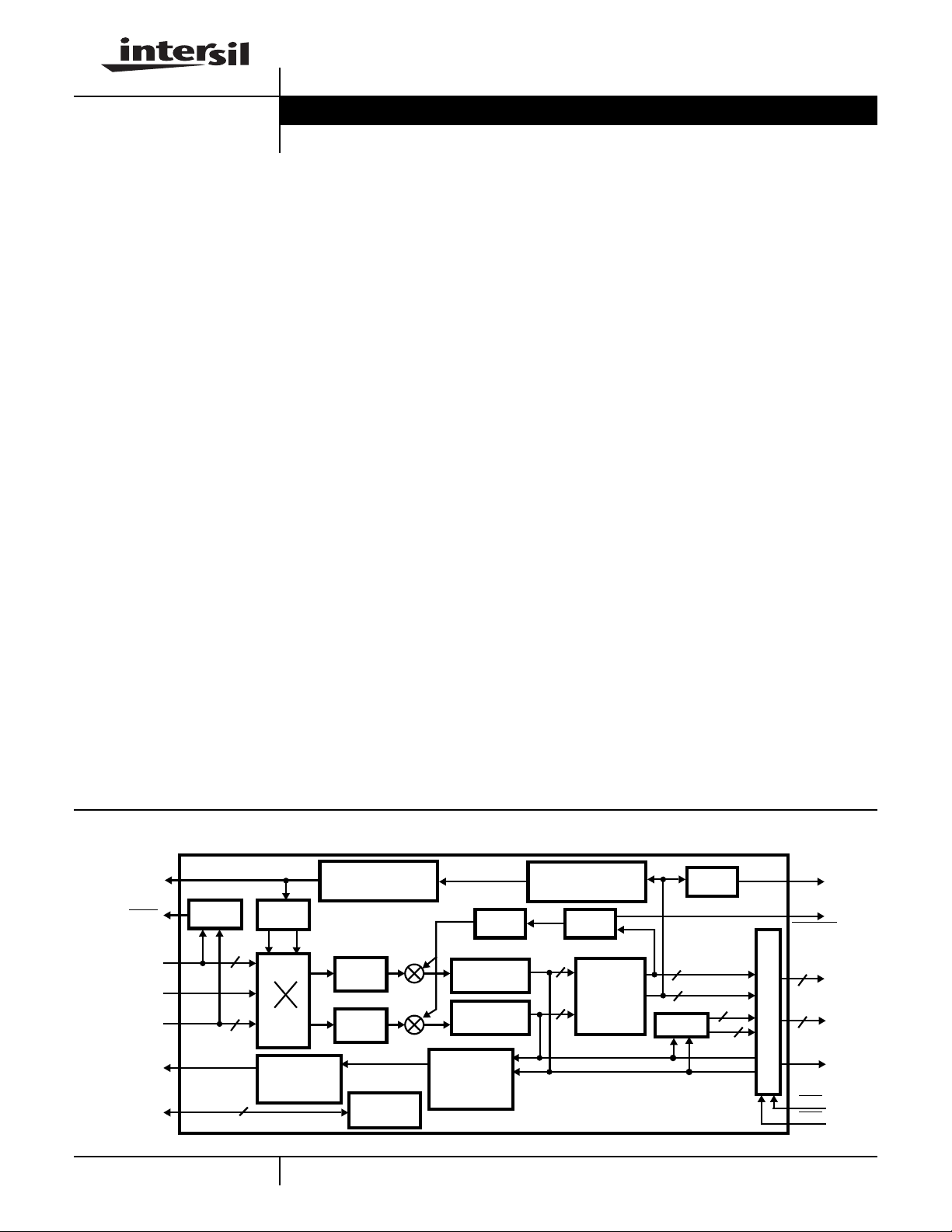
Block Diagram
CARRIER
TRACK
CONTROL
HI/LO
I SER OR
(9-0)
I
IN
SERCLK
OR CLK
Q SER OR
Q
(9-0)
IN
SYMBOL
TRACK
CONTROL
CONTROL/
STATUS
BUS
(COF)
(SOF)
LEVEL
DETECT
COS
10
10
13
3-253
NCO
SIN
I
Q
SYMBOL
TRACKING
LOOP FILTER
CARRIER ACQ/TRK
LOOP FILTER
RRC
FILTER
RRC
FILTER
CONTROL
INTERFACE
CAUTION: These devices are sensitive to electrostatic discharge; follow proper IC Handling Procedures.
CARRIER PHASE
ERROR DETECT
LOOP
FILTER
INTEGRATE/
DUMP
INTEGRATE/
DUMP
SYMBOL
PHASE
ERROR
DETECT
http://www.intersil.com or 407-727-9207
LEVEL
DETECT
8
CARTESIAN
8
TO
POLAR
LOCK
DETECT
MAGNITUDE
8
8
SLICER
PHASE
3
3
Q
I
LKINT
THRESH
A
OUT(9-0)
10
10
B
OUT(9-0)
DATA PATH MULTIPLEXER
SMBLCLK
OEA
OEB
| Copyright © Intersil Corporation 1999
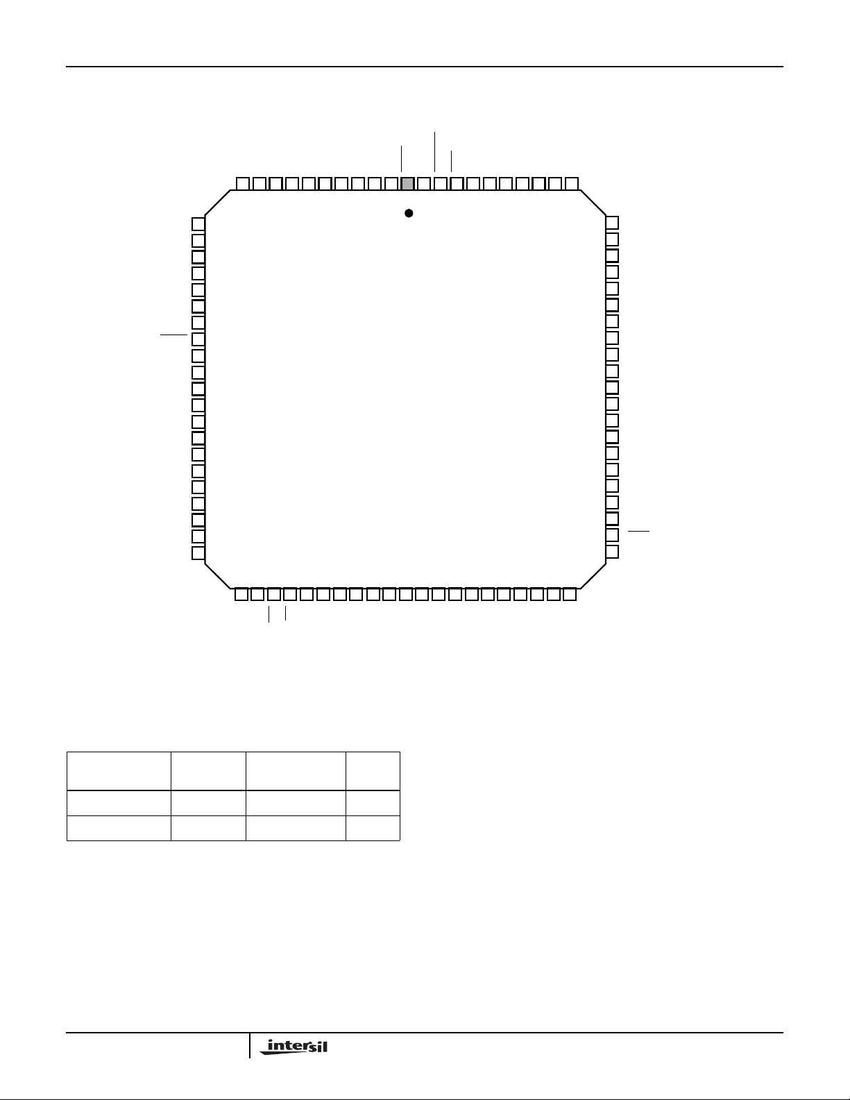
Pinout
IIN6
IIN7
IIN8
IIN9
GND
SERCLK
VCC
SSYNC
HSP50210
84 LEAD PLCC
TOP VIEW
SLOCLK
HI/LO
ISER
QSER
OEA
THRESH
AOUT8
AOUT9
AOUT7
GND
AOUT6
AOUT5
757677787980818283841234567891011
AOUT4
IIN5
IIN4
IIN3
IIN2
GND
IIN1
IIN0
SYNC
QIN9
QIN8
QIN7
QIN6
QIN5
QIN4
VCC
QIN3
QIN2
QIN1
QIN0
SOFSYNC
SOF
12
13
14
15
16
17
18
19
20
21
22
23
24
25
26
27
28
29
30
31
32
WR
COF
COFSYNC
RD
GND
A2
A1
A0
C7
C6
C5
C4
C3
VCC
C2
C1
C0
FZ-ST
FZ-CT
LKINT
535251504948474645444342414039383736353433
GND
74
73
72
71
70
69
68
67
66
65
64
63
62
61
60
59
58
57
56
55
54
AOUT3
AOUT2
AOUT1
AOUT0
SMBLCLK
VCC
CLK
GND
BOUT9
BOUT8
BOUT7
BOUT6
BOUT5
GND
BOUT4
BOUT3
BOUT2
BOUT1
BOUT0
OEB
VCC
Ordering Information
TEMP.
PART NUMBER
RANGE (oC) PACKAGE
HSP50210JC-52 0 to 70 84 Lead PLCC N84.1.15
HSP50210JI-52 -40 to 85 84 Lead PLCC N84.1.15
3-254
PKG.
NO.
HSP50210
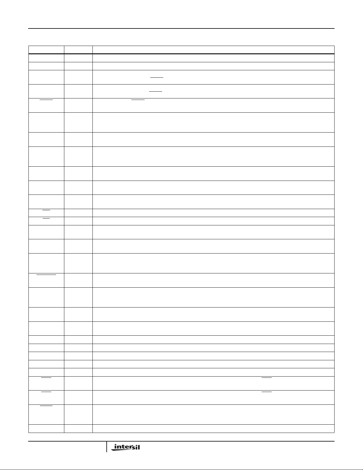
Pin Description
NAME TYPE DESCRIPTION
V
CC
GND - Ground.
IIN9-0 I In-Phase Parallel Input. Data may be two’s complement or offset binary format (see Table 14). These inputs are
QIN9-0 I Quadrature Parallel Input. Data may be two’s complement or offset binary format (see Table 14). These inputs are
SYNC I Data Sync. When SYNC is asserted “Low”, data on IIN9-0 and QIN9-0 is clocked into the processing pipeline by the
COF O Carrier Offset Frequency. The frequency term generated by the Carrier TrackingLoop Filter is output serially via this
COFSYNC O Carrier Offset Frequency Sync. This signal is asserted one CLK or SLOCLK cycle before the MSB of the serial data
SOF O Sampler Offset Frequency. Sample frequency correction term generatedbytheSymbol TrackingLoopFilterisoutput
SOFSYNC O Sampler Offset Frequency Sync. This signal is asserted one CLK or SLOCLK cycle before the MSB of the serial
A2-0 I AddressBus.Theaddress on these pins specify a target register for reading or writing (see Microprocessor Interface
C7-0 I/O Microprocessor Interface Data Bus. This bi-directional bus is used for reading and writing to the processor interface.
WR I Write. This is the write strobe for the processor interface (see Microprocessor Interface Section).
RD I Read. This is the read enable for the processor interface (see Microprocessor Interface Section).
FZ_ST I Freeze Symbol Tracking Loop. Asserting this pin “high” zeroes the sampling error into the Symbol Tracking Loop
FZ_CT I Freeze Carrier Tracking Loop. Asserting this pin “high” zeroes the carrier Phase Error input to the Carrier Tracking
LKINT O Lock Detect Interrupt. This pin is asserted “high” for at least 4 CLK cycles when the Lock Detector Integration cycle
THRESH O Threshold Exceeded. This output is asserted “low” when the magnitude out of the Cartesian to Polar converter
SLOCLK O Slow Clock. Optional serial clock used for outputting data from the Carrier and Symbol Tracking Loop Filters. The
ISER I In-Phase Serial Input. Serial data input forIn-Phase Data. Data on this pin is shifted in MSB first and is synchronous
QSER I Quadrature Serial Input. Serial data input for Quadrature Data. Data on this pin is shifted in MSB first and is
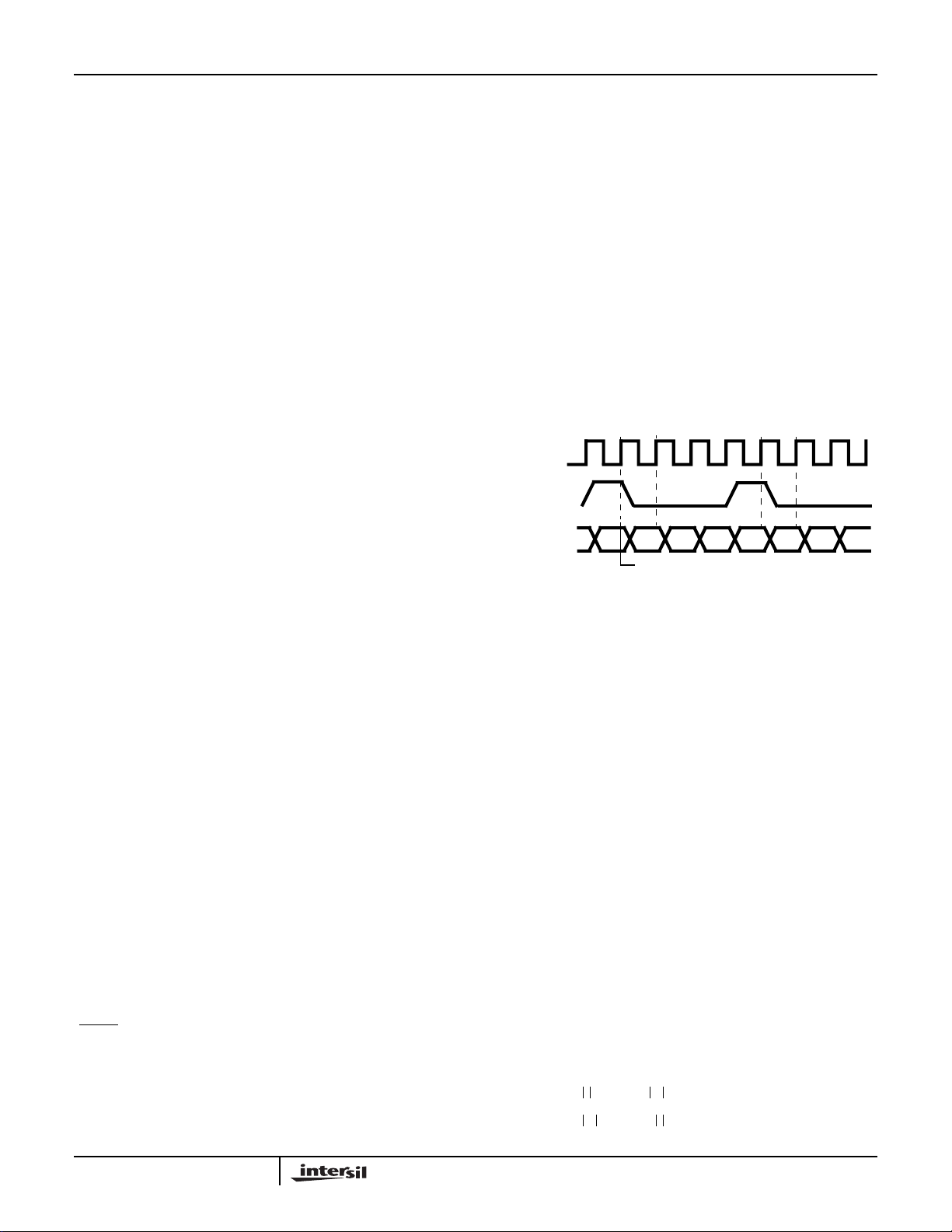
SSYNC I Serial Word Sync. This input is asserted “high” one CLK before the first data bit of the serial word (see Figure 2).
SERCLK I Serial Clock. May be asynchronous to other clocks. Used to clock in serial data (see Input Controller Section).
AOUT9-0 O A Output. Data on this output depend on the configuration of Output Selector . AOUT9 is the MSB (see Table 42).
BOUT9-0 O B Output. Data on this output depend on the configuration of Output Selector . BOUT9 is the MSB (see Table 42).
SMBLCLK O Symbol Clock. 50% duty cycle clock aligned with soft bit decisions (see Figure 19).
OEA I A Output Enable. This pin is the three-state control pin for the AOUT9-0. When OEA is high, the AOUT9-0 is high
OEB I B Output Enable. This pin is the three-state control pin for the BOUT9-0. When OEB is high, the AOUT9-0 is high
HI/LO 0 HI/LO. The output of the Input Level Detector is provided on this pin (see Input Level Detector Section). This signal
CLK I System Clock. Asynchronous to the processor interface and serial inputs.
- +5V Power Supply.
sampled by CLK when the SYNC signal is active Low. IIN9 is the MSB. See Input Controller Section.
sampled by CLK when the
rising edge of CLK.
pin. The new offset frequency is shifted out MSB first by CLK or SLOCLK starting with the clock cycle after the
assertion of COFSYNC.
word. (Programmable Polarity, see Table 41, bit 11).
serially via this pin. The frequency word is shifted out MSB first by CLK or SLOCLK starting with the clock cycle after
assertion of SOFSYNC.
data word. (Programmable Polarity, see Table 41, bit 12).
Section). A0 is the LSB.
These are the data I/O pins for the processor interface. C0 is the LSB.
Filter (see Symbol Tracking Loop Filter Section).
Loop Filter.
is finished (see Lock Detector Section). Used as an interrupt for a processor. The Lock Detect Interrupt may be
asserted “high” longer than 4 CLK cycles, depending on the Lock Detector mode.
exceeds the programmable Power Detect Threshold (see Table 15 and AGC Section).
clock is programmable and has a 50% duty cycle.
SYNC signal is active Low. QIN9 is the MSB. See Input Controller Section.
Note: Not used when the HSP50110 is used with the
HSP50210 (see Table 41).
to SERCLK (see Input Controller Section).
synchronous to SERCLK (see Input Controller Section).
impedance.
impedance.
can be externally averaged and used to control the gain of an amplifier to close an AGC loop around the A/D converter. This type of AGC sets the level based on the median value on the input.
3-255
3-256
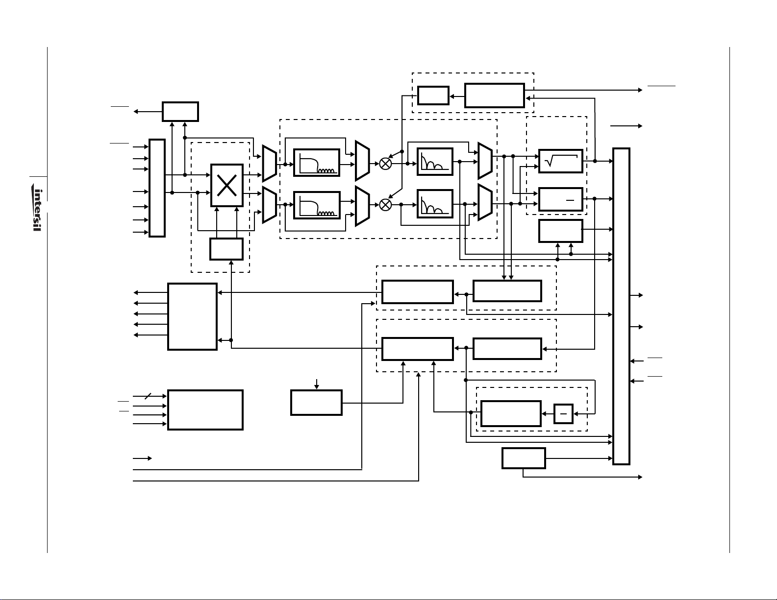
HI/LO
SYNC
IIN9-0
QIN9-0
SSYNC
SERCLK
ISER
QSER
LEVEL
DETECT
INPUT CONTROLLER
I
Q
SYNTHESIZER/
MIXER
SIN
COS
NCO
AGC
LOOP
FILTER
MATCHED FILTERING
M
U
X
M
U
X
RRC
RRC
M
U
X
M
U
X
I&D
I&D
GAIN ERROR
DETECT
M
U
X
M
U
X
CARTESIAN
TO
POLAR
I2+Q
Q
TAN-1( )
SLICER
2
I
THRESH
SMBLCLK
SOFSYNC
SOF
COFSYNC
COF
SLOCLK
C7-0
WR
RD
A2-0
CLK
FRZ_ST
FRZ_CT
FORMATTER
8
MICROPROCESSOR
SERIAL
OUTPUT
INTERFACE
SYMBOL TRACKING
SYMBOL PHASE
ERROR DETECT
CARRIER PHASE
ERROR DETECT
DISCRIMINATOR
FREQUENCY
ERROR DETECT
FROM
LOCK
DETECTOR
ACQUISITION
CONTROL
2ND ORDER LOOP
FILTER
CARRIER TRACKING
2ND ORDER LOOP
FILTER
FIGURE 1. FUNCTIONAL BLOCK DIAGRAM OF THE HSP50210
LOCK
DETECT
HSP50210
AOUT9-0
BOUT9-0
OEA
OEB
d
dt
LKINT
HSP50210
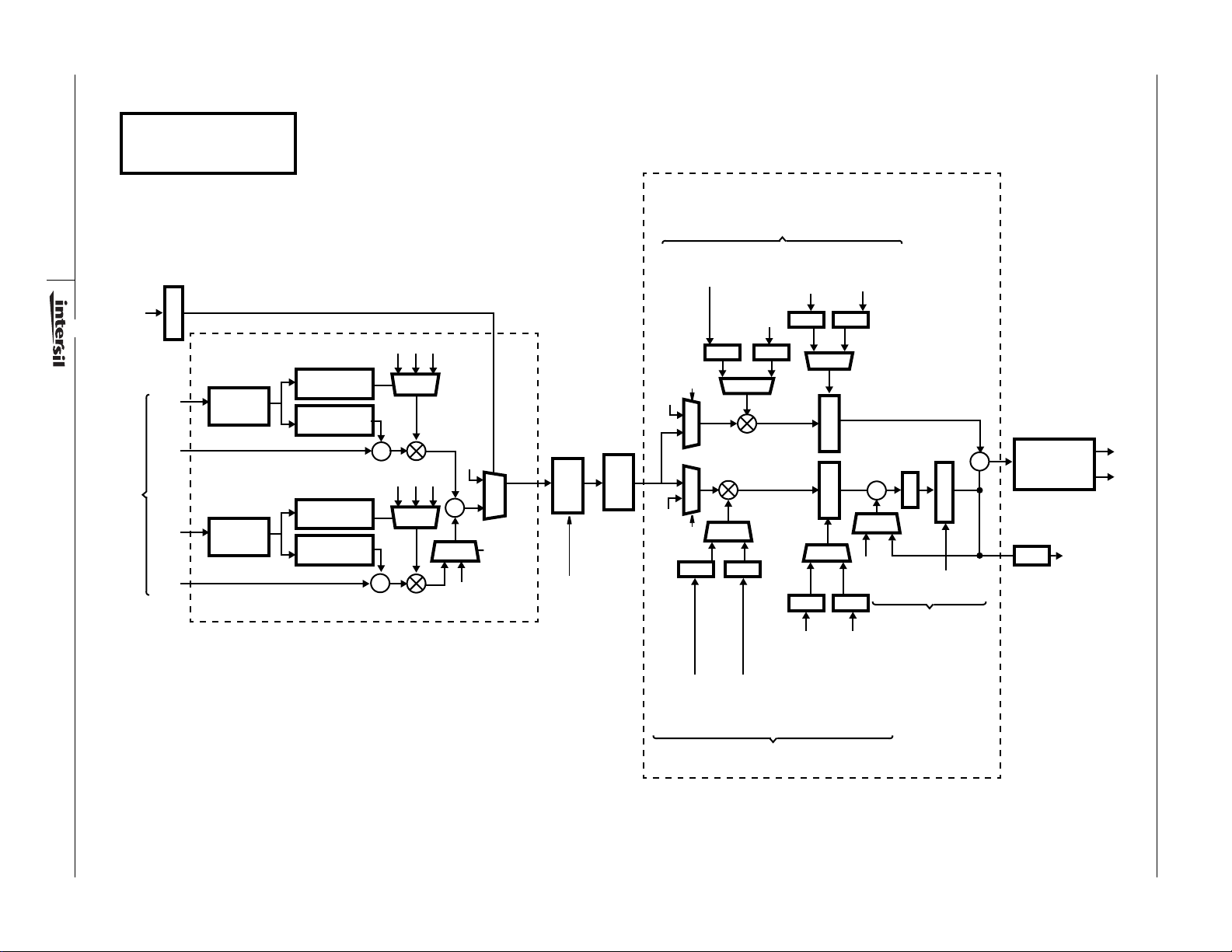
Functional Description
The HSP50210 Digital Costas Loop (DCL) contains most of
the baseband processing functions needed to implement a
digital Costas Loop Demodulator. These functions include
LO generation/mixing, matched filtering, AGC, carrier phase
and frequency error detection, timing error detection, carrier
loop filtering, bit sync loop filtering, lock detection,
acquisition/tracking control, and soft decision slicing for
forward error correction algorithms. While the DCL is
designed to work with the HSP50110 Digital Quadrature
Tuner (DQT) as a variable rate PSK demodulator for satellite
demodulation, functions on the chip are common to many
communications receivers.
The DCL provides the processing blocks for the three
tracking loops commonly found in a data demodulator: the
Automatic Gain Control (AGC) loop, the Carrier Tracking
Loop, and a Symbol Tracking Loop. The AGC loop adjusts
for input signal power variations caused by path loss or
signal-to-noise variations. The carrier tracking loop removes
the frequency and phase uncertainties in the carrier due to
oscillator inaccuracies and doppler. The symbol tracking
loop removes the frequency and phase uncertainties in the
data and generates a recovered clock synchronous with the
receiveddata. Each loop consists of an error detector,a loop
filter, and a frequency or gain adjustment/control. The AGC
loop is internal to the DCL, while the symbol and carrier
tracking loops are closed external to the DCL. When the
DCL is used together with the HSP50110, the tracking loops
are closed around the baseband filtering to center the signal
in the filter bandwidth. In addition, the AGC function is
divided between the two chips with the HSP50110 providing
the coarse AGC, and the HSP50210 providing the fine or
final AGC.
A top level block diagram of the HSP50210 is shown in
Figure 1. This diagram shows the major blocks and the
multiplexers used to reconfigure the data path for various
architectures.
Input Controller
In-Phase (I) and Quadrature (Q) data enters the part through
the Input Controller. The 10-bit data enters in either serial or
parallel fashion using either two’s complement or offset
binary format. The input mode and binary format is set in the
Data Path Configuration Control Register, bits 14 and 15
(see Table 14).
If Parallel Input mode is selected, I and Q data are clocked
into the part through IIN0-9 and QIN0-9 respectively. Data
enters the processing pipeline when the input enable
(
SYNC) is sampled “low” by the processing clock (CLK). The
enable signal is pipelined with the data to the various
processing elements to minimize pipeline delay where
possible. As a result, the pipeline delay through the AGC,
Carrier Tracking, and Symbol Tracking Loop Filters is
measured in CLKs; not input data samples.
If serial input mode is selected, the I and Q data enters via
the ISER and QSER pins using SERCLK and SSYNC. The
beginning of a serial word is designated by asserting
SSYNC ‘high’ one SERCLK prior to the first data bit, as
shown in Figure 2. On the following SERCLK’s, data is
shifted into the register until all 10 bits havebeen input. Data
shifting is then disabled and the contents of the register are
held until the next assertion of SSYNC. The assertion of a
SSYNC transfers data into the processing pipeline, and the
Shift Register is enabled to accept new data on the following
SERCLK. When data is transferred to the processing
pipeline by SSYNC, a processing enable is generated which
follows the data through the pipeline. This enable allows the
delaythrough processing elements (likethe loop filters) to be
minimized since their pipeline delay is expressed in CLKs
not SSYNC periods.
Note: SSYNC should not be
asserted for more than one SERCLK cycle.
SERCLK
SSYNC
ISER/
QSER
NOTE: Data must be loaded MSB first.
FIGURE 2. SERIAL INPUT TIMING FOR ISER AND QSER INPUTS
MSB
SSYNC LEADS 1st DATA BIT
MSB
Input Level Detector
The Input Level Detector generates a one-bit error signal for
an external IF AGC filter and amplifier. The error signal is
generated by comparing the magnitude of the input samples
to a user programmable threshold. The HI/LO pin is then
driven “high” or “low” depending on the relationship of its
magnitude to the threshold. The sense of the HI/LO pin is
programmable so that a magnitude exceeding the threshold
can either be represented as a “high” or “low” logic state.
The Input Level Detector (HI/LO output) threshold and the
sense are set by the Data Path Configuration Control
Register bits 16-23 and 13 (see Table 14).
Level Detector is typically not used in applications
which use the HSP50210 with the HSP50110.
The high/low outputs can be integrated by an external loop
filter to close an AGC loop. Using this method, the gain of
the loop forces the median magnitude of the input samples
to the threshold. When the magnitude of half of the samples
is above the threshold (and half is below), the error signal is
integrated to zero by the loop filter.
The magnitude of the complex input is estimated by:
Mag (I, Q) I 0.375 Q if I Q and>×+=
Mag (I, Q) Q 0.375 I if Q I>×+=
Note: The Input
(EQ. 1)
3-257
REGISTER ENABLE RATE
@ = SYNC RATE
= TWICE SYMBOL RATE
*
! = SYMBOL RATE
BLANK = CLK RATE
MID AND END
SYMBOL SAMPLES
TO SYMBOL TRACKING
I
MID
I
END
Q
MID
Q
END
3-258
HI/LO
REG
REG
DETECT
IIN9-0QIN9-0
LEVEL
NCO MIXER
COMPLEX
MULTIPLY
SIN
REG REG
REG REG
SIN/COS
ROM
REG
REG
BYPASS
MIXER
COS
+
R
E
G
R
E
G
R
R
E
E
G
G
R
R
E
E
G
G
CF
REGISTER
MATCHED FILTERING
M
U
X
15 TAP RRC
@
15 TAP RRC
@
ROOT RAISED COSINE
BYPASS
RRC
(RRC)
D
FALSE LOCK
REG
DATA DE-SKEW
DUMP
+
M
U
R
R
X
E
E
G
G
R
R
E
E
G
G
R
L
E
I
G
M
R
I
E
T
G
DUMP
R
E
G
R
E
G
AGC LOOP FILTER
R
E
G
@ OR !
UPPER
GAIN
LIMIT
+
L
I
M
I
T
LOWER
GAIN
LIMIT
OQPSK
“0”
M
U
X
R
E
G
M
U
X
M
U
R
X
E
G
@
*
“0”
S
R
H
E
F
G
T
@
INTEGRATE AND DUMP
R
E
+
G
LOOP GAIN
EXPONENT
COMPARE
S
R
H
I
E
F
G
T
*
TWO SAMPLE
SUMMER
R
I
E
G
*
S
R
H
E
I
G
F
T
LOOP GAIN
MANTISSA
BYPASS
I&D
+
M
U
X
+
HOLD AGC
M
U
X
E
M
U
X
D
E
M
U
X
M
U
X
AGC ERROR DETECT
“0”
AGC THRESHOLD
GAIN
ERROR
POWER
THRESHOLD
CARTESIAN TO
POLAR
2
I2+Q
Q
-1
TAN
( )
I
PHASE OUT AT
MAG OUT AT
-
+
COMPARE
SOFT
DECISION
SLICER
TEST
5
DELAY
REG
5
DELAY
REG
@ OR
@ OR !
M
U
X
R
E
G
R
E
G
R
E
G
R
E
G
O
R
U
E
T
**
G
P
R
U
! OR ! OR
E
T
G
S
E
L
E
8
C
T
8
AOUT9-0 BOUT9-0
R
E
G
R
E
G
HSP50210
*
TO
CARRIER
TRACKING
AND
DISCRIMINATOR
THRESH
R
E
G
FROM CARRIER TRACKING
LOOP FILTER
FIGURE 3. MAIN DATA PATH

HSP50210
NCO/Mixer
The NCO/Mixer performs a complex multiply between the
baseband input and the output of a quadrature NCO
(Numerically Controlled Oscillator). When the HSP50210
(DQT) is used with the HSP50110 (DCL), the NCO/Mixer
shortens the Carrier Tracking Loop (i.e., minimizes pipeline
delay around the loop) while providing wide loop
bandwidths. This becomes important when operating at
symbol rates near the maximum range of the part.
There are three configurations possible for closing the
Carrier Tracking Loop when the DQT and the DCL are used
together.The first configuration utilizes the NCO on the DQT
and bypasses the NCO in the DCL. The Data Path
Configuration Control Register (see Table 14), bit 10, and
Carrier Loop Filter Control Register #1 (see Table 20), bit 6,
are used to bypass the DCL NCO/Mixer and route the Loop
filter outputs, respectively. The DQT provides maximum
flexibility in NCO control with respect to frequency and
phase offsets.
The second configuration feeds the lead Carrier Loop filter
term to the DCL NCO/Mixer, and the lag Loop filter Term to
the DQT NCO. This reduces the loop transport delay while
maintaining wide loop bandwidths and reasonable loop
damping factors. This configuration is especially useful in
SATCOM applications with medium to high symbol rates.
The Carrier Loop Filter Control Register #1, bit 5, is where
the lead/lag destination is set.
The final configuration feeds both the lead and lag Carrier
Loop Filter terms back to the DCL NCO/Mixer. This provides
the shortest transport delay. The DCL NCO/Mixer provides
only for frequency/phase control from the Carrier Loop filter.
The center frequency of this NCO/Mixer is set to the average
of the Upper and Lower Carrier Loop Limits programmable
parameters. These parameters are set in the two control
registers bearing their names (see Tables 22 and 23).
The NCO/Mixer uses a complex multiplier to multiply the
baseband input by the output of a quadrature NCO. This
operation is represented by:
I
OUTIIN
Q
OUTIIN
Equation 3 illustrates how the complex multiplier implicitly
performs the summing function when the DCL is configured
as a modulator. The quadrature outputs of the NCO are
generated by driving a sine/cosine look-up table with the
output of a phase accumulator as shown in Figure 3. Each
time the phase accumulator is clocked, its sum is
incremented by the contents of the Carrier Frequency (CF)
Register. As the accumulator sum increments from 0 to 2
the SIN/COS ROM produces quadrature outputs whose
phase advances from 0 to 360
32-bit phase increment which is updated with the output of
ωC()cos Q
ωC()sin Q
IN
ωC()sin–=
ωC()cos+=
IN
o
. The CF Register contains a
(EQ. 2)
(EQ. 3)
32
Carrier Tracking Loop. Large phase increments take fewer
clocks to step through the sine wave cycle, which results in a
higher frequency NCO output.
The CF Register sets the NCO frequency with the following
equation:
FCf
CF INT FCf
where f
CF()2⁄
×=
CLK
[]H=
is the CLK frequency, and CF is the 32-bit two’s
CLK
32
⁄()2
CLK
32
(EQ. 4)
complement hexadecimal value loaded into the Carrier
Frequency Register. As an example, if the CF Register is
loaded with a value of 4000 0000 (Hex), and the CLK
frequency is 40MHz, the NCO would produce quadrature
terms with a frequency of 10MHz. When CF is a negative
value, a clockwise cos/sin vector rotation is produced. When
CF is positive, a counterclockwise vector rotation is
produced.
NOTE: The NCO is set to a fixed frequency by programming the
upper and lower limits of the Carrier Tracking Loop Filter to the
same value and zeroing the lead gain.
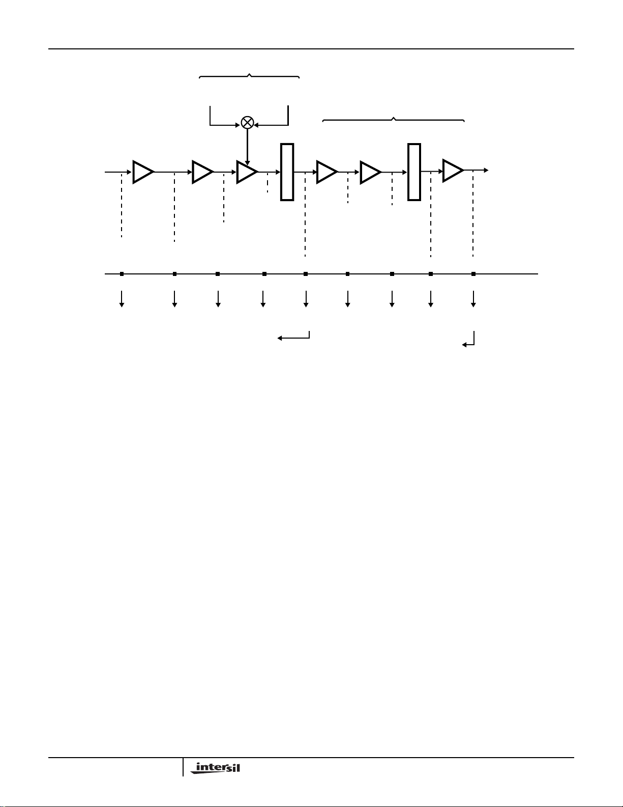
Matched Filtering
The HSP50210 provides two selectable matched filters: a
Root Raised Cosine Filter (RRC) and an Integrate and
Dump (I&D) filter. These are shown in Figure 3. The RRC
filter is provided for shaped data pulses and the I&D filter is
provided for square wave data. The filters may be cascaded
for better adjacent channel rejection for square wave data. If
these two filters do not meet baseband filtering
requirements, then they can be bypassed and an external
digital filter (such as the HSP43168 Dual FIR Filter or the
HSP43124 Serial I/O Filter) used to implement the desired
matched filter. The desired filter configuration is set in the
Data Path Configuration Control Register, bits 1-7 (see
Table 14).
The sample rate of the baseband input depends on the
symbol rate and filtering configuration chosen. In
configurations which bypass both filters or use only the RRC
Filter,the input sample rate must be twice the symbol rate. In
configurations which use the I&D Filter,the input sample rate
is decimated by the I&D Filter, down to two samples per
symbol. I&D configurations support input sample rates up to
32 times the input symbol rate.
The RRC filter is a fixed coefficient 15 Tap FIR filter. It has
~40% excess bandwidth beyond Nyquist which equates to
α = ~0.4 shape factor. The filter frequency response is
shown in Figure 4 and Figure 5. In addition, the 9-bit filter
,
coefficients are listed as integer values in Table 1. The noise
equivalent bandwidth of the RRC filter and other filter
configurations possible with the HSP50110/210 chipset are
given in Appendix A.
3-259
HSP50210
0
-20
-40
-60
-80
NORMALIZED MAGNITUDE (dB)
-100
0
f
CLK
10
FREQUENCY (NORMALIZED TO INPUT SAMPLE RATE)
2f
CLK
10
3f
CLK
10
FIGURE 4. RRC FILTER IN HSP50210
0
-0.18
-0.36
SHOWN BELOW
-0.54
-0.72
NORMALIZED MAGNITUDE (dB)
-0.90
0
0
-0.07
-0.14
-0.21
-0.28
NORMALIZED MAGNITUDE (dB)
-0.35
0
FREQUENCY (NORMALIZED TO INPUT SAMPLE RATE)
ENLARGED FOR CLARITY
f
CLK
2f
CLK
25
3f
20
f
CLK
f
CLK
25
40
CLK
40
3f
CLK
25
f
CLK
10
TABLE 1. ROOT RAISED COSINE COEFFICIENTS
COEFFICIENT INDEX COEFFICIENT
02
1-2
21
38
4 -16
5 -14
4f
CLK
10
f
CLK
2
686
7 160
886
9 -14
10 -16
11 8
12 1
13 -2
14 2
The I&D filter consists of an accumulator, a programmable
shifter and a two sample summer as shown in Figure 3. The
programmable shifter is provided to compensate for the gain
introduced by the accumulator (see Table 14). The
accumulator provides Integrate and Dump Filtering for
decimation factors up to 16. The two sample summer
4f
CLK
25
f
CLK
5
provides the moving average required for an additional
decimation factor of 2. A decimation factor of 1 (bypass), 2,
4, 8, 16, or 32 may be selected. At the maximum decimation
rate, a baseband signal sampled at 32 times the symbol rate
can be filtered.
The output of the two sample summer is demultiplexed into
two sample streams at the symbol rate. The demultiplexed
data streams from the I and Q processing paths are fed to
the Symbol Tracking Block and Soft decision slicer. The
multiplexed data streams on I and Q are provided as one of
the selectable inputs for the Cartesian to Polar Converter.
Cartesian/Polar Converter
3f
5f
CLK
40
CLK
20
The Cartesian/PolarConverter maps samples on the I and Q
processing paths to their equivalent phase/magnitude
representation. The magnitude conversion is equivalent to:
FIGURE 5. PASSBAND RIPPLE OF RRC FILTER IN HSP50210
3-260
Mag (I, Q) 0.81()∗I2Q2+(),=
(EQ. 5)
where 0.81 is the gain of the conversion process. The
magnitude output is an 8-bit unsigned value ranging from 0.0
to 1.9922.
HSP50210
The phase conversion is equivalent to:
Phase (I, Q) tan
where tan
-1
( ) is the arctangent function. The phase
1–
QI⁄(),=
(EQ. 6)
conversion output is an 8-bit two’s complement output which
ranges from -1.0 to 0.9922 (80 to 7f HEX, respectively). The
-1 to almost 1 range of the phase output represents phase
values from -πto π, respectively. An example of the I/Q to
phase mapping is shown in Figure 6. The phase and
magnitude values may be output via the Output Selector bits
0-3 (see Table 42).
1.0
0.5
0
MAGNITUDE
-0.5
-1.0
-π
FIGURE 6A. I INPUT TO CARTESIAN/POLAR CONVERTER
1.0
0.5
0
MAGNITUDE
-0.5
-1.0
-π
FIGURE 6B. Q INPUT TO CARTESIAN/POLAR CONVERTER
1.0
0.5
0
OUTPUT VOLTAGE
-0.5
-1.0
-π
FIGURE 6C. CARTESIAN/POLAR CONVERTER PHASE OUTPUT
-π/2
-π/2
-π/2
0
INPUT PHASE
0
INPUT PHASE
0
INPUT PHASE
π/2
π/2
π/2
The I/Q data path selected for input to the Cartesian to Polar
converter determines the input data rate of the AGC and
carrier tracking loops. If the I/Q data path out of the Integrate
and Dump Filter is selected, the AGC is fed with magnitude
values produced by the end-symbol samples. Magnitude
values produced by midsymbol samples are not used
because these samples occur on symbol transitions, resulting
in poor signal magnitude estimates. The Carrier Tracking
block is fed with phase values generated from both the end
and mid-symbol samples. The carrier tracking loop filter ,
howev er, is only fed with Phase Error terms generated by the
end symbol samples. If the input of the I&D is selected for
input to the coordinate converter, the control loops are f ed
with data at the I/Q data rate. The desired data path input to
the Cartesian to Polar converter is specified in the Data Path
Configuration Control Register, bit 8 (see Table 14).
AGC
The AGC loop operates on the main data path (I and Q) and
performs three signal level adjusting functions: 1)
maximizing dynamic range, 2) compensating for SNR
variations, and 3) maintaining an optimal level into the Soft
Decision Slicer. The AGC Loop Block Diagram, shown in
π
π
π
Figure 7, consists of an Error Detector, a Loop Filter, and
Signal Gain Adjusters (multipliers). The AGC Error Detector
generates an error signal by subtracting the programmable
AGC threshold from the magnitude output of the Cartesian
to Polar Converter. This difference signal is scaled (gain
adjusted via multiplier and shifter), then filtered (integrated)
by the AGC Loop Filter to generate the gain correction to the
I and Q signals at the multipliers. If a fixed gain is desired,
set the upper and lower limits equal.
The AGC responds to the magnitude of the sum of all the
signals in the bandpass of the narrowest filter preceding the
Cartesian to Polar Coordinate Converter. This filter may be
the Integrate and Dump filter shown in Figure 8, the RRC
filter upstream in the HSP50210 data path, or some other
filter outside the DCL chip. The magnitude signal usually
contains several components: 1) the signal of interest
component, 2) the noise component, and 3) interfering
signals component. At high SNR’s the signal of interest is
significantly greater than the other components. At lower
SNR’s, components 2 or 3 may become greater than the
signal of interest. Narrowing the filter bandwidth is the
primary technique used to mitigate magnitude contributions
of component 3. This will also improve the SNR by
reducing the magnitude contributions of element 2.
Consideration of the range of signal amplitudes expected
into the HSP50210, in conjunction with a gain distribution
analysis, will provide the necessar y insight to set the signal
level into the Soft Decision Slicer to yield optimum
performance.
Note: Failure to consider the variations
due to noise or interfering signals, can result in signal
limiting in the HSP50210 processing algorithms, which
will degrade the system Bit Error Rate performance.
3-261
HSP50210
The AGC Loop is configured by the PowerDetect Threshold
and AGC Loop Parameters Control Registers (see Tables 15
and 16). Seven programmable parameters must be set to
configure the AGC Loop and its status outputs. Two
parameters, the Power Threshold and the AGC Threshold
are associated with the Error Detector and are represented
in 8-bit fractional unsigned binary format: 2
-7.
5
2-62
. While the format provides a range from 0 - 1.9961
0.2-12-22-32-42-
for the thresholds, the Cartesian to Polar Converter scales
the I and Q input magnitudes by 0.81. Thus, if a full scale
(±1) complex (I and Q) input signal is presented to the
converter,the output will be √(0.81)
2
+ (0.81)2= 1.1455. The
AGC Threshold parameter value is the desired magnitude of
the signal as it enters the Soft Decision Slicer. It is the
parameter that will determine the error signal in the AGC
loop. The Power Threshold, on the other hand, determines
only the power threshold at which the
THRESH signal is
asserted. If the signal magnitude exceeds the threshold,
then the
THRESH is asserted. This may be used for signal
detection, power detection or external AGC around the A/D
converter. The AGC Threshold parameter is set in the AGC
Loop Parameters Control Register,bits 16-23 (see Table 16).
The Power Threshold parameter is set in the Power Detect
Threshold Control Register, bits 0-7 (see Table 15). Note
that these two threshold parameters are not required to be
set to identical or even related values, since they perform
independent functions
The Enable AGC parameter sets the AGC Error Detector
output to zero if asserted and to normal error detection
output when not asserted. This control bit is set in the AGC
Loop ParameterControl Register, bit 31 (see Table 16). This
bit is used to disable the AGC loop.
The remaining AGC parameters determine the AGC loop
characteristics: gain tracking, tracking rate and tracking limits.
The AGC Loop gain is set via two parameters: A GC Loop
Gain Exponent and AGC Loop Gain Mantissa. In general, the
higher the loop gain, the faster signal level acquisition and
tracking, but this must be tempered b y the specific signal
characteristics of the application and the remaining
programmable loop parameters. For the HSP50210, the AGC
Loop Gain provides for a variab le atten uation of the input to
the loop filter. The A GC gain mantissa is a 4-bit value which
provides error signal scaling from 0.000 to 0.9375, with a
resolution of 0.0625. Table 2 details the discrete set of
decimal values possible forthe AGC Loop Gain mantissa. The
-7
exponent provides a shift factor scaling from 2
to 2
-14
.
Table 3 details the discrete set of decimal values possible for
the AGC Loop Gain Exponent. When combined, the exponent
and mantissa provide a loop gain defined as:
AGC Loop Gain: G
AGC
M()24–()[]2
()[]=
7E+()–
(EQ. 7)
Register, bits 24-30 (see Table 16). The composite range of
the AGC loop Gain is 0.0000 to [0.9375][2-7]. This will scale
the AGC error signal to a range of 0.000 to
(1.1455)(0.9375)(2-7) = 1.07297(2-7).
TABLE 2. AGC LOOP GAIN BINARY MANTISSA TO DECIMAL
SCALED MANTISSA MAPPING
BINARY
CODE
(MMMM)
0000 0.0000 1000 0.5000
0001 0.0625 1001 0.5625
0010 0.1250 1010 0.6250
0011 0.1875 1011 0.6875
0100 0.2500 1100 0.7500
0101 0.3125 1101 0.8125
0110 0.3750 1110 0.8750
0111 0.4375 1111 0.9375
TABLE 3. AGC LOOP BINARY EXPONENT TO SCALED
BINARY CODE
(EEE)
000 0 2
001 1 2
010 2 2
011 3 2
100 4 2
101 5 2
110 6 2
111 7 2
DECIMAL
SCALED
MANTISSA
DECIMAL EXPONENT MAPPING
DECIMAL/ HEX
EXPONENT
BINARY
CODE
(MMMM)
DECIMAL SCALED
DECIMAL
SCALED
MANTISSA
EXPONENT
-7
-8
-9
-10
-11
-12
-13
-14
where M is a binary number with a range from 0 to 15 and E
is a 3-bit binary value from 0 to 7. M and E are the
parameters set in the AGC Loop Parameters Control
3-262
HSP50210
READ
REG
AGC GAIN = (1.0 + M) x 2
GAIN
ADJUST
G
AGC
I
Q
AGC LOOP FILTER
AGC
AGC
UPPER
E
LOWER
LIMIT †
LIMIT †
L
R
I
E
M
G
I
T
1.0000 TO 15.8572 = G
(0 TO 24dB)
AGC LOOP
GAIN
MANTISSA †
-7
TO 2
(2
S
R
H
I
E
+
0.000 TO 1.07297(2
L
I
M
I
T
F
G
T
AGC
CART/POLAR INPUT SELECT†
AGC LOOP
EXPONENT †
-14
(0.000 TO 0.9375)
)
R
E
G
-7
)
I&D FILTER
I&D FILTER
GAIN
M
U
X
“0”
ENABLE AGC †
M
U
X
AGC ERROR DETECT
COMPARE
POWER
THRSHLD †
+
G
TAN
-
1.64
-----------=
I2+Q
-1
( )
GAIN
ERROR
AGC THRSHLD †
CARTESIAN TO POLAR
1.0
R
E
THRESH
G
1.64
dcloutlvl agc thresh
=
----------- -
2
where dcloutlvl is the
2
2
Q
I
magnitude output expressed
in dB from Full Scale (dBFS)
0.8
MAGNITUDE
(0 - 1.1455)
PHASE
† Indicates a microprocessor control signal.
FIGURE 7. AGC LOOP BLOCK DIAGRAM
The AGC Loop Filter integrates the scaled error signal to
provide a correction control term to the multipliers in the I and
Q path. The loop filter accumulator has internal upper and
lower limiters. The upper eight bits of the accumulator output
map to an exponent and mantissa format that is used to set
these upper and lower limits. The format, illustrated in Figure
8, is used for the AGC Upper Limit, AGC Lower Limit and the
Correction Control Term(AGC output). This format should not
be confused with the similar format used for the AGC Loop
Gain. The input to the AGC Loop Filter is included in Figure 8
to show the relative weighting of the input to output of the loop
filter. The loop filter input is represented as the ele ven letter
“G”s. Lower case “e” and “m” detail the format f or the AGC
Upper and LowerLimits. This change in type case should help
keep the AGC Limits and A GC Gain formats from being
confused. The AGC Upper and Lower Limits are set in the
AGC Loop Parameters Control Register, bits 0-15, (see Table
16). This 6-bit unsigned mantissa format provides for an AGC
output control range from 0.0000 to 0.9844, with a resolution
of 0.015625. The 2-bit exponent format provides an A GC
output control range from 1 to 8. The decimal values for each
of the 64 binary mantissa values is detailed in Table 4, while
Table 5 details the decimal value for the 4 exponent values .
The AGC Output is implemented in the multiplier according
to Equation 8.
Out
Out
AGC linear–
AGC dB–
1.0 m
+()2e()=
AGC
20 log 1.0 m
+()2e()[]=
AGC
(EQ. 8A)
(EQ. 8B)
where m and e are the binary values for mantissa and
exponent found in Tables 4 and 5.
NOTE:Thisformat is identical to the format used to program the
AGC Upper and Lower Limits, but in this usage it is not a programmed value. It is a representation of the digital AGC output
number which is presented to the Gain Adjuster (multipliers) to
correct the gain of the I and Q data signals in the main data path.
These equations yield a composite (mantissa and
exponent) AGC output range of 0.0000 to 1.9844(2
3
) which
is a logarithmic range from 0 to 24dB. Figure 9 has graphed
the results of Equation 8 for both the linear and logar ithmic
equations. Figure 9 also has a linear estimate of the
logarithmic equation. This linear approximation will be used
in calculating the AGC response time.
120.2-12-22-32-42-52-62-72-82-92-102-112-122-132-142-152-162-172-18
2
ee.mmmmm m
GGGG GGGGGG G
FIGURE 8. AGC OUTPUT AND AGC LIMITS BIT WEIGHTING
3-263
HSP50210
TABLE 4. AGC GAIN MANTISSA TO DECIMAL MAPPING
DECIMAL
VALUE
BINARY CODE
(MMMMMM
TABLE 5. AGC GAIN EXPONENT TO DECIMAL MAPPING
BINARY CODE
AGC
000000 0.000000 100000 0.500000
000001 0.015625 100001 0.515625
000010 0.031250 100010 0.531250
000011 0.046875 100011 0.546875
000100 0.062500 100100 0.562500
000101 0.078125 100101 0.578125
000110 0.093750 100110 0.593750
000111 0.109375 100111 0.609375
001000 0.125000 101000 0.625000
001001 0.140625 101001 0.640625
001010 0.156250 101010 0.656250
001011 0.171875 101011 0.671875
001100 0.187500 101100 0.687500
001101 0.203125 101101 0.703125
001110 0.218750 101110 0.718750
001111 0.234375 101111 0.734375
010000 0.250000 110000 0.750000
010001 0.265625 110001 0.765625
010010 0.281250 110010 0.781250
010011 0.296875 110011 0.796875
010100 0.312500 110100 0.812500
010101 0.328125 110101 0.828125
010110 0.343750 110110 0.843750
010111 0.359375 110111 0.859375
011000 0.375000 111000 0.875000
011001 0.390625 111001 0.890625
011010 0.406250 111010 0.906250
011011 0.421875 111011 0.921875
011100 0.437500 111100 0.937500
011101 0.453125 111101 0.953125
011110 0.468750 111110 0.968750
011111 0.484375 111111 0.984375
00 0 2
01 1 2
10 2 2
11 3 2
OF AGC
)
MANTISSA
BINARY CODE
(MMMMMM
DECIMAL/ HEX
EXPONENT
DECIMAL SCALED
)
AGC
EXPONENT
DECIMAL
VALUE
OF AGC
MANTISSA
0
1
2
3
224
240
24
18
12
6
0
256
16
12
LINEAR ESTIMATE IN dB
8
4
DATA PATH GAIN (LINEAR)
1
0
0
1632486480
(8 MSBs OF LOOP FILTER ACCUMULATOR)
FIGURE 9. GAIN CONTROL TRANSFER FUNCTION
GAIN dB
96
112
128
144
GAIN CONTROL WORD
160
176
192
GAIN
LINEAR
208
There are two techniques for setting a fixed gain for the
AGC. The first is to set Control Word 2 bit 31 = 1. This
precludes any error update of present AGC gain value.The
second is to set the upper and lower AGC limits to the
desired gain using Figure 9. The upper and lower limits
have the same value for this case.
The HSP50210 provides two mechanisms for monitoring
signal strength. The first, which involved the THRESH
signal, has already been described. The second
mechanism is via the Microprocessor Interface. The 8 most
significant bits of the AGC loop filter output can be read by
a microprocessor. Refer to the Microprocessor Interface
Section for details of how to read this value. This AGC
value has the format described in Figure 8.
AGC Bit Weighting and Loop Response
The AGC loop response is a function of the programmable
gain, the bit weightings inherent in the connection of each
element of the loop, the AGC Loop filter limits and the
magnitude of the input gain error step. Table 6 details the bit
weighting between each element of the AGC Loop from the
error detector through the weighting at the gain adjuster in
the signal path. The AGC Loop Gain sets the growth rate of
the sum in the loop filter accumulator. The Loop filter output
growth rate determines how quickly the AGC loop traces the
transfer function shown previously in Figure 9. To calculate
the rate at which the AGC can adjust over a given period of
time, a gain step is introduced to the gain error detector and
the amount of change that is observed between clocks at the
AGC Level Adjusters (multipliers) is the AGC response time
in dB per symbol.This AGC loop will respond immediately
with the greatest correction term, then asymptotically
approach zero correction.
We begin calculation of the loop response with a full scale
error detector input of ±1. This error input is scaled by the
Cartesian to Polar converter, the error detector and the AGC
Loop Gain, accumulated in the loop filter,limited and output to
the gain adjusters. The AGC loop tries to make the error
correction as quickly as possible, but is limited by the AGC
GAIN (dB)
3-264
HSP50210
Loop Gain and potentially,the AGC limits. The maximum AGC
response is the maximum gain adjustment made in any given
clock cycle. This inv olves applying maximum Loop gain and
setting the AGC limits as wide as possible. A calculation using
TABLE 6. AGC BIT WEIGHTING
AGC LOOP
AGC
ACCUM
BIT
POSITION
22 Shifter → E1 12
21 Shifter → E0 6
20 Multiplier → M-1 3
19 M -2 1.5
18 M -3 0.75
17 M -4 0.375
16 M -5 0.1875
15 Multiplier → 1 M -6 0.09375
14
13 1 G -8 0.02344
12 2 G -9 0.01172
11 3 G -10 0.00586
10 4 G -11 0.00293
9 5 G -12 0.00146
8 8(S) = 1(S) 0. 12(S) 12(S) = 1 1 6 G -13 0.000732
7 7 = 0• x1111= 0•
6 6 = 1 x 10 10 = 1 1 G -15 0.000183
5 5 = 2 x 9 9 = 2 2 G -16 0.0000916
4 4 = 3 x 8 8 = 3 3 G -17 0.0000458
3 3 = 4 7 7 = 4 4 G -18 0.0000229
2 2 = 5 6 6 = 5 5 -19 0.0000114
1 1 = 6 5 5 = 6 6 -20 0.00000572
0 0 = 7 4 -21 0.00000286
GAIN
ERROR
INPUT
GAIN
ERROR
BIT
WEIGHT
AGC LOOP
FILTER GAIN
(MANTISSA)
FILTER
GAIN
MULIPLIER
(OUTPUT)
3
2
1
0
only exponent terms of the various gains will be sufficient to
yield a rough order of magnitude of the range of the AGC
Loop response. The results are shaded in the last column of
Table 6 and provided in detail in Equations 9A and 9B.
AGC
LOOP
FILTER
GAIN BITS
KEPT
(rnd)
SHIFT
= 0
0• G -14 0.000366
SHIFT
= 7
0• • 0-7 0.04688
AGC
OUTPUT
AND AGC
LIMITS BIT
WEIGHT
RESOLUTION
AGC GAIN
(dB)
AGC Response
AGC Response
where (0.5) is the MSB of the 0.81 scaling in the Cartesian to Polar Coordinate Converter, (0.5) is the MSB of the mantissa of the
Loop Gain, (2
= Input (Cartesian to Polar Converter Gain)(Error Detector Gain)(AGC Loop Gain)(AGC Output Weighting)
MAX
= ±1(0.5)(0.5)(2-7)(24) = ±1(2-9)(24) = 0.04688dB/symbol time
MAX
-7
) is the maximum shift gain, and 24 is the maximum loop filter gain.
(EQ. 9A)
A similar procedure is used to calculate the minimum AGC response rate.
AGC Response
= ±1(0.5)(0.5)(2
MIN
-14
)(24) = ±1(2
-16
)(24) = 0.000366dB/symbol time
(EQ. 9B)
Thus, the expected range for the AGC rate is approximately 0.0004 to 0.0469dB/symbol time.
3-265
MANTISSA
1.0 - 1.9844
(0.0156 STEPS)
G = 1.0 - 1.9844*2
AGC GAIN
HSP50210
EXPONENT
0-23
2
3
INTEGRATE AND
DUMP FILTER
INT/DUMP
SHIFTER
0
-4
G = 2
- 2
4
-2
3
2
2
2
1
2
0
2
-1
2
-7
2
IF INT/DUMP OUTPUT SELECTED
4
-2
3
2
2
2
1
2
0
2
-1
2
-11
2
SAMPLE PAIR
G = 0.5, 1.0 (NOTE 3)
L
I
M
I
T
0
-2
-1
2
-6
2
SUMMER
-2
2
2
2
INPUT TO
SOFT DECISION
SLICER
AND
SYMBOL TRACKING
BLOCK
0
-1
-6
-7
NOTES:
SYNTHESIZER/
MIXER
G = 1.0, 0.5 (NOTE 1)
PART
INPUT
0
BINARY
POINT
-2
-1
2
-9
2
INPUT TO CARTESIAN TO POLAR CONVERTER
(NOTE 4)
RRC
FILTER
G = 1.0, 1.13 (NOTE 2)
1
0
-2
-1
2
-10
2
RND
IF AGC OUTPUT SELECTED
-2
0
2
-1
2
-10
2
RND
INT/DUMP
ACCUMULATOR
G = 1-16
L
I
8
M
/
G
AGC
I
T
5
-2
4
2
3
2
2
2
1
2
0
2
-1
2
-9
2
0
-2
-1
2
-7
2
RND
INPUT TO CARTESIAN TO POLAR CONVERTER
1. If the Mixer is enabled the result of the complex multiply is scaled by two (G = 0.5). If the mixer is b ypassed, the data passes unmodified (G = 1.0).
2. If the Root Raised Cosine Filter is enabled, a gain of G = 1.13 is introduced. If the RRC filters bypassed, the gain is unity.
3. If the integrate and Dump Filter is bypassed the Sample Pair summer has a gain of G = 1.0 and the 2-7-bit position is set to 1. If the integrate
and dump is enabled, the sample pair sum is scaled by one half (G = 0.5).
4. The negative sign on the MSBs indicates use of 2’s complement data format.
FIGURE 10. GAIN DISTRIBUTION AND INTERMEDIATE BIT WEIGHTINGS
Gain Distribution
The gain distribution in the DCL is shown in Figure 10.
These gains consist of a combination of fixed,
programmable, and adaptive gains. The fixed gains are
introduced by processing elements such as the Mixer and
Square Root of Root Raised Cosine Filter. The adaptive
gains are set to compensate for variations in input signal
strength.
The main signal path, with processing block gains and path
bit weightings, is shown in Figure 10. The quadrature inputs
to the HSP50210 are 10-bit fractional two’s complement
numbers with relative bit weightings, as shown in the
Figure 10. The first element in the processing chain is the
Mixer, which scales the quadrature outputs of the complex
multiplier by 1/2 providing a gain of G = 0.5. If the Mixer is
bypassed, the signal is passed unmodified with a gain of 1.0.
Following the mixer, the quadrature signal is passed to the
fixed coefficient RRC filtering block, which has a gain of 1.13
if enabled and 1.0 if bypassed. Next, the AGC supplies gain
to maintain an optimal signal level at the input to the Soft
Decision Slicer, Cartesian to Polar Converter, and the
Symbol Tracking Loop. The gain supplied by the AGC
ranges from 1.0 to 1.9844*2
3
.
Following the A GC, the signal path is limited to 8 bits and
passed through the Integrate and Dump Filter en route to the
Soft Decision Slicer and Symbol TrackingBlock.The I&D Filter
uses an accumulator together with a sample pair summer to
achieve the desired decimation rate . The I&D shifter is
provided to compensate for the gain introduced by the I&D
Accumulator. The accumulator introduces gain equal to the
decimation factor R, and the shifter gain can be set to 1/R. For
example, if the I&D Filter decimation of 16 is chosen the I&D
Accumulator will accumulate 8 samples before dumping,
which produces a gain of 8. Thus, for unity gain, the I&D
-3
Shifter would be set for a gain of 2
. The Sample Pair
Summer is unity gain since its output is scaled by one-half.
Symbol Tracking
The symbol tracking loop adjusts the baseband sampling
frequency to force sampling of the baseband waveform at
optimal points for data decisions. The ke y elements of this
loop are the Sampling Error Detector and Symbol Tracking
Loop Filter shown in Figure 11. The output of these two blocks
is a frequency correction term which is used to adjust the
baseband sample frequency external to the HSP50210. In
typical applications, the frequency correction term is fed back
to the HSP50110 to adjust baseband sampling via the
Resampling NCO (see HSP50110 Datasheet).
3-266
3-267
REGISTER ENABLE RATE
! = SYMBOL RATE
BLANK = CLK RATE
SYMBOL TRACK
LOOP FILTER
LEAD GAIN
FRZ_ST
END
MID
!
MID AND END
Q
SYMBOL SAMPLES
END
Q
MID
R
E
G
SAMPLING ERROR DETECTOR
I
I
DAT A
DECISION
MID-SYMBOL
DAT A
DECISION
MID-SYMBOL
TRANSITION
DETECT
TRANSITION
MID-POINT
TRANSITION
DETECT
TRANSITION
MID-POINT
LEAD
MANTISSA
ACQ
MANTISSA
TRACK
‘0’ ‘-1’‘1’
MUX
ZERO
LEAD
“0”
REG REG
MUX
-
+
“0”
‘0’ ‘-1’‘1’
‘0’
MUX
SINGLE/
DOUBLE
RAIL
SAMPLING
MUX
-
+
+
MUX
ERROR
INVERT
INVERT
ERROR
!
ERROR
ACCUM.
“0”
ZERO
LAG
REG REG
LAG
MANTISSA
ACQ
MUX MUX
MUX
LAG
MANTISSA
TRACK
EXPONENT
LEAD
EXPONENT
LEAD
ACQ
REG
REG
MUX
SHIFT SHIFT
MUX
REG REG
LAG
LAG
ACQ
EXPONENT
TRACK
LEAD
EXPONENT
TRACK
+
MUX
LOAD
ACC
ACCUMULATOR
REG
LIMIT
ACC LIMITS
UPPER/LOWER
LAG
+
SERIAL
OUTPUT
FORMATTER
SOFSYNC
REG
TO
µP
INTERFACE
SOF
HSP50210
FIGURE 11. SYMBOL TRACKING
LAG GAIN
 Loading...