

Intersil Corporation HSP50110 Datasheet

HSP50110
Data Sheet January 1999 File Number
Digital Quadrature Tuner
The Digital Quadrature Tuner (DQT) provides many of the
functions required for digital demodulation. These functions
include carrier LO generation and mixing, baseband
sampling, programmable bandwidth filtering, baseband AGC,
and IF AGCerror detection. Serial control inputs are provided
which can be used to interface with external symbol and
carrier tracking loops. These elements make the DQT ideal
for demodulator applications with multiple operational modes
or data rates. The DQT may be used with HSP50210 Digital
Costas Loop to function as a demodulator for BPSK, QPSK,
8-PSK OQPSK, FSK, FM, and AM signals.
The DQT processes a real or complex input digitized at rates
up to 52 MSPS. The channel of interest is shifted to DC by a
complex multiplication with the internal LO. The quadrature
LO is generated by a numerically controlled oscillator (NCO)
with a tuning resolution of 0.012Hz at a 52MHz sample rate.
The output of the complex multiplier is gain corrected and fed
into identical low pass FIR filters. Each filter is comprised of a
decimating low pass filter followed by an optional
compensation filter. The decimating low pass filter is a 3
stage Cascaded-Integrator-Comb (CIC) filter. The CIC filter
can be configured as an integrate and dump filter or a third
order CIC filter with a (sin(X)/X)
filters are provided to flatten the (sin(X)/X)
CIC. If none of the filtering options are desired, they may be
bypassed. The filter bandwidth is set by the decimation rate of
the CIC filter. The decimation rate may be fixed or adjusted
dynamically by a symbol tracking loop to synchronize the
output samples to symbol boundaries. The decimation rate
may range from 1-4096. An internal AGC loop is provided to
maintain the output magnitude at a desired level. Also, an
input level detector can be used to supply error signal for an
external IF AGC loop closed around the A/D.
The DQT output is provided in either serial or parallel formats
to support interfacing with a variety DSP processors or digital
filter components. This device is configurable o ver a general
purpose 8-bit parallel bidirectional microprocessor control bus.
3
response. Compensation
N
response of the
3651.4
Features
• Input Sample Rates to 52 MSPS
• Internal AGC Loop for Output Level Stability
• Parallel or Serial Output Data Formats
• 10-Bit Real or Complex Inputs
• Bidirectional 8-Bit Microprocessor Interface
• Frequency Selectivity <0.013Hz
• Low Pass Filter Configurable as Three Stage CascadedIntegrator-Comb (CIC), Integrate and Dump, or Bypass
• Fixed Decimation from 1-4096, or Adjusted by NCO
Synchronization with Baseband Waveforms
• Input Level Detection for External IF AGC Loop
• Designed to Operate with HSP50210 Digital Costas Loop
• 84 Lead PLCC
Applications
• Satellite Receivers and Modems
• Complex Upconversion/Modulation
• Tuner for Digital Demodulators
• Digital PLL’s
• Related Products: HSP50210 Digital Costas Loop;
A/D Products HI5703, HI5746, HI5766
• HSP50110/210EVAL Digital Demod Evaluation Board
Ordering Information
TEMP.
PART NUMBER
HSP50110JC-52 0 to 70 84 Ld PLCC N84.1.15
HSP50110JI-52 -40 to 85 84 Ld PLCC N84.1.15
RANGE (oC) PACKAGE PKG. NO.
Block Diagram
10
REAL OR COMPLEX
INPUT DATA
10
IF AGC
CONTROL
CONTROL/STATUS
BUS
LEVEL
DETECT
3-229
COMPLEX
MULTIPLIER
8
LOOP
LOW PASS FIR
FILTER
o
o
NCO
LOW PASS FIR
FILTER
FILTER
RE-SAMPLING
http://www.intersil.com or 407-727-9207
GCA
90
0
GCA
PROGRAMMABLE
CONTROL
INTERFACE
CAUTION: These devices are sensitive to electrostatic discharge; follow proper IC Handling Procedures.
NCO
LEVEL
DETECT
DUMP
10
I DATA
CARRIER
TRACKING CONTROL
10
Q DATA
SAMPLE STROBE
SAMPLE RATE
CONTROL
| Copyright © Intersil Corporation 1999
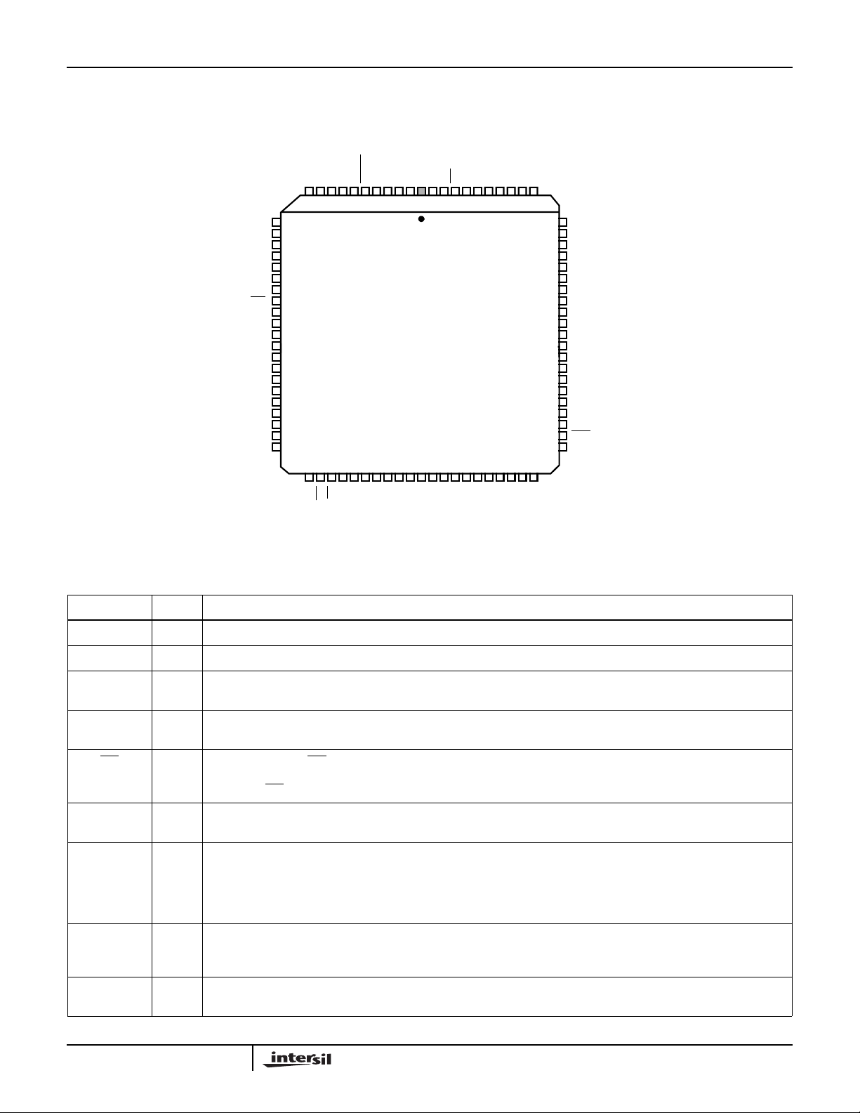
Pinout
IIN5
IIN4
IIN3
IIN2
GND
IIN1
IIN0
ENI
QIN9
QIN8
QIN7
QIN6
QIN5
QIN4
V
QIN3
QIN2
QIN1
QIN0
PH1
PH0
HSP50110
HSP50110 (PLCC)
TOP VIEW
IOUT4
IOUT5
IOUT6
GND
IOUT7
IOUT8
IOUT9
OEI
LOTP
SPH0
SPH1
SPH2
SPH3
VCCSPH4
SSTRB
HI/LO
IIN9
IIN8
IIN7
IIN6
111098765432184838281807978777675
12
13
14
15
16
17
18
19
20
21
22
23
24
25
26
CC
27
28
29
30
31
32
33 343536 37 38 39 40 41 42 43 44 45 46 47 48 49 50 51 52 53
74
73
72
71
70
69
68
67
66
65
64
63
62
61
60
59
58
57
56
55
54
IOUT3
IOUT2
IOUT1
IOUT0
DATARDY
V
CC
CLK
GND
QOUT9
QOUT8
QOUT7
QOUT6
QOUT5
GND
QOUT4
QOUT3
QOUT2
QOUT1
QOUT0
OEQ
V
CC
CFLD
WR
GND
V
COF
COFSYNC
SOF
SOFSYNC
GND
CC
C0
C1
C2
C3
C4
C5
C6
C7
A0
A1
A2
RD
Pin Description
NAME TYPE DESCRIPTION
V
CC
GND - Ground.
IIN9-0 I In-Phase Input. Data input for in-phase (real) samples. Format may be either two’s complement or offset binary format
QIN9-0 I Quadrature Input. Data input for quadrature (imaginary) samples. Format may be either two’s complement or offset bi-
ENI I Input Enable. When ENI is active ‘low’, data on IIN9-0 and QIN9-0 is clocked into the processing pipeline by the rising
PH1-0 I Carrier Phase Offset. The phase of the internally generated carrier frequency may be shifted by 0, 90, 180, or 270 de-
CFLD I Carrier Frequency Load. This input loads the Carrier Frequency Register in the Synthesizer NCO (see
- +5V Power Supply.
(see I/O Formatting/Control Register in Table 10). IIN9 is the MSB.
nary format (see I/O Formatting/Control Register in Table 10). QIN9 is the MSB.
edge of CLK. This input also controls the internal data processing as described in the Input Controller Section of the
data sheet. ENI is active ‘low’.
grees bycontrolling these pins (see Synthesizer/Mixer Section). The phase mapping for these inputs is givenin Table 1.
Synthesizer/Mixer Section). When this input is sampled ‘high’ by clock, the contents of the Microprocessor Interface
Holding Registers are transferred to the carrier frequency register in the Synthesizer NCO (see Microprocessor Interface Section).
NOTE: This pin must be ‘low’ when loading other configuration data via the Microprocessor In-
terface. Active high Input.
COF I Carrier Offset Frequency Input. This serial input is used to load the Carrier Offset Frequency into the Synthesizer NCO
(see Serial Interface Section). The new offset frequency is shifted in MSB first by CLK starting with the clock cycle after
the assertion of COFSYNC.
COFSYNC I Carrier Offset FrequencySync.This signal is asserted one CLK cycle before the MSB of the offset frequency data word
(see Serial Interface Section).
3-230

HSP50110
Pin Description
NAME TYPE DESCRIPTION
SOF I Sampler Offset Frequency. This serial input is used to load the Sampler Offset Frequency into the Re-Sampler NCO
SOFSYNC I Sampler Offset Frequency Sync. This signal is asserted one CLK cycle before the MSB of Sampler Offset Frequency
A2-0 I Address Bus. These inputs specify a target register within the Microprocessor Interface (see Table 5). A2 is the MSB.
C7-0 I/0 Control Bus. This is the bidirectional data bus for reads and writes to the Microprocessor Interface (see Microprocessor
WR I Write. This is the write strobe for the Microprocessor Interface (see Microprocessor Interface Section).
RD I Read. This is the read enable for the Microprocessor Interface (see Microprocessor Interface Section).
IOUT9-0 O In-Phase Output. The data on these pins is output synchronous to CLK. New data on IOUT9-0 is indicated by the as-
QOUT9-0 O Quadrature Output. The data on these pins is output synchronous to CLK. New data on the QOUT(9-0) pins is indicated
DATARDY O Data Ready. This output is asserted on the first clock cycle that new data is available on the IOUT and QOUT data
(Continued)
(see Serial Interface Section). The new offset frequency is shifted in MSB first by CLK starting with the clock cycle after
assertion of SOFSYNC.
data word (see Serial Interface Section).
This input is setup and held to the rising edge of WR.
Interface Section). C7 is the MSB.
sertion of the DATARDYpin. Data may be output parallel or serial mode (see Output Formatter Section). In the parallel
mode, IOUT9 is the MSB. When the serial mode is used, IOUT0 is data, and IOUT9 is the serial clock. Other pins not
used in serial mode may be set high or low via the control interface.
by the DATARDY pin. Data may be output parallel or serial mode. In the parallel mode, IOUT9 is the MSB. When the
serial mode is used, QOUT0 is data.
busses (see Output Formatter Section). This pin may be active ‘high’ or ‘low’ depending on the configuration of the I/O
Formatting/Control Register (see Table10). In serial mode, DATARDYis asserted one IQ clock before for first bit of serial data.
OEI I In-Phase Output Enable. This pin is the three-state control for IOUT9-0. When OEI is ‘high’, the IOUT bus is held in the
high impedance state.
OEQ I Quadrature Output Enable. This pin is the three-state control for QOUT9-0. When OEQ is ‘high’, the QOUT bus is held
in the high impedance state.
LOTP 0 LocalOscillator Test Point. This output is the MSB of the Synthesizer NCO phase accumulator (see Synthesizer/Mixer
Section). This is provided as a test point for monitoring the frequency of the Synthesizer NCO.
SSTRB 0 Sample Strobe. This is the bit rate strobe for the bit rate NCO. SSTRB has two modes of operation: continuous update
and sampled. In continuous update mode, this is the carry output of the Re-Sampler NCO. In sampled mode, SSTRB
is active synchronous to the DATARDY signal for parallel output mode. The sampled mode is provided to signal the
nearest output sample aligned with or following the symbol boundary.This signal can be used with SPH(4-0) below to
control a resampling filter to time shift its impulse response to align with the symbol boundaries.
SPH4-0 0 Sample Phase. These are five of the most significant 8 bits of the Re-Sampler NCO phase accumulator. Which five bits
of the eight is selected via the Chip Configuration Register (see Table 12). These pins update continuously when the
SSTRB output is in the continuous update mode. When the SSTRB pin is in the sampled mode, SPH4-0 update only
when the SSTRB pin is asserted. In the sampled mode, these pins indicate how far the bit phase has advanced past
the symbol boundary when the output sample updates. SPH4 is the MSB.
HI/LO 0 HI/LO. The output of the Input Level Detector is provided on this pin (see Input Level Detector Section). The sense of
the HI/LO pin is set via the Chip Configuration Register (see Table 12). This signal can be externally averagedandused
to control the gain of an amplifier to close an AGC loop around the A/D converter. This type of AGC sets the level based
on the median value on the input.
CLK I Clock. All I/O’s with the exception of the output enables and the microprocessor interface are synchronous to clock.
3-231

HSP50110
HI/LO
IIN0-9
CLK
QIN0-9
ENI
INPUT MODE†
INPUT FORMAT†
COFSYNC
WORD WIDTH†
SOFSYNC
LEVEL
DETECT
10
10
PH0-1
CFLD
COF
COF EN†
SOF
A0-2
WR
RD
C0-7
HI/LO OUTPUT SENSE†
THRESHOLD FOR
EXTERNAL AGC†
SYNTHESIZER/MIXER
INPUT
CONTROLLER
SHIFT REG
MULTIPLIER
COS SIN
SYNTHESIZER
MICROPROCESSOR INTERFACE
COMPLEX
10
NCO
UPPER LIMIT†
LOWER LIMIT†
LOOP
AGC
12
12
10
32
CENTER
FREQUENCY†
8
PHASE
OFFSET†
LOTP
FILTER
LOW PASS FILTERING
DECIMATING COMPENSATION
FILTER FILTER
CLK
†
Indicates data downloaded via microprocessor interface
LOOP GAIN †
11
11
DIVIDER
RE-SAMPLER
NCO
SHIFT REG
RE-SAMPLER
AGC THRESHOLD†
10
10
5
32
SAMPLER CENTER
FREQUENCY†
SOF EN†
WORD WIDTH†
LEVEL
DETECT
F
O
R
M
A
T
OEI
IOUT0-9
DATARDY
QOUT0-9
OEQ
SSTRB
SPH0-4
FIGURE 1. FUNCTIONAL BLOCK DIAGRAM OF HSP50110
Functional Description
The Digital Quadrature Tuner (DQT) provides many of the
functions needed for digital demodulation including: carrier
LO generation, mixing, low-pass filtering, baseband
sampling, baseband AGC, and IF AGC error detection. A
block diagram of the DQT is provided in Figure 1. The DQT
processes a real or complex input at rates up to 52 MSPS.
The digitized IF is input to the Synthesizer/Mixer where it is
multiplied by a quadrature LO of user programmable
frequency. This operation tunes the channel of interest to DC
where it is extracted by the Low Pass FIR Filtering section.
The filter bandwidth is set through a user programmable
decimation factor. The decimation factor is set by the ReSampler which controls the baseband sampling rate. The
baseband sample rate can be adjusted by an external
symbol tracking loop via a serial interface. Similarly, a serial
interface is provided which allows the frequency of the
Synthesizer/Mixer’s NCO to be controlled by an external
carrier tracking loop. The serial interfaces were designed to
mate with the output of loop filters on the HSP50210 Digital
Costas Loop.
The DQT provides an input level detector and an internal
AGC to help maintain the input and output signal
magnitudes at user specified levels. The input level detector
compares the input signal magnitude to a programmable
level and generates an error signal. The error signal can be
externally averaged to set the gain of an amplifier in front of
the A/D which closes the AGC loop. The output signal level
is maintained by an internal AGC loop closed around the
Low Pass Filtering. The AGC loop gain and gain limits are
programmable.
Input Controller
The input controller sets the input sample rate of the
processing elements. The controller has two operational
modes which include a Gated Input Mode for processing
sample rates slower than CLK, and an Interpolated Input
Mode for increasing the effective time resolution of the
samples. The mode is selected by setting bit 1 of the I/O
Formatting Control Register in Table 10.
In Gated Input Mode, the Input Enable (
data flow into the input pipeline and the processing of the
internal elements. When this input is sampled “low” by CLK,
the data on IIN0-9 and QIN0-9 is clocked into the processing
pipeline; when
ENI is sampled “high”, the data inputs are
disabled. The Input Enable is pipelined to the internal
ENI) controls the
3-232

HSP50110
processing elements so that they are enabled once for each
time
ENI is sampled low. This mode minimizes the
processing pipeline latency, and the latency of the part’s
serial interfaces while conserving power.
Note: the
effective input sample rate to the internal processing
elements is equal to the frequency with which
ENI is
asserted “low”.
In Interpolated Input Mode, the ENI input is used to insert
zeroes between the input data samples. This process
increases the input sample rate to the processing elements
which improves the time resolution of the processing chain.
When
ENI is sampled “high” by CLK, a zero is input into the
processing pipeline. When
data is fed into the pipeline.
ENI is sampled “low” the input
Note: Due to the nature of the
rate change operation, consideration must be given to
the scaling and interpolation filtering required for a
particular rate change factor.
In either the Gated or Interpolated Input Mode, the
Synthesizer NCO is gated by the
ENI input. This only allows
clocking of the NCO when external samples are input to the
processing pipeline. As a result, the NCO frequency must be
set relative to the input sample rate, not the CLK rate (see
Synthesizer/Mixer Section).
NOTE: Only fixed
interpolation rates should be used when operating the
part in Interpolated Mode at the Input Controller.
Input Level Detector
The Input Level Detector generates a one-bit error signal for
an external IF AGC filter and amp. The error signal is
generated by comparing the magnitude of the input samples
to a user programmable threshold. The HI/LO pin is then
driven “high” or “low” depending the relationship of its
magnitude to the threshold. The sense of the HI/LO pin is
programmable so that a magnitude exceeding the threshold
can either be represented as a “high” or “low” logic state.
The threshold and the sense of the HI/LO pin are configured
by loading the appropriate control registers via the
Microprocessor Interface (see Tables 8 and 12).
The high/low outputs can be integrated by an external loop
filter to close an AGC loop. Using this method the gain of the
loop forces the median magnitude of the input samples to
the threshold. When the magnitude of half the samples are
above the threshold and half are below, the error signal is
integrated to zero by the loop filter.
6.5%. For real inputs, the magnitude detector reduces to a
an absolute value detector with negligible error.
Note: an external AGC loop using the Input Level
Detector may go unstable for a real sine wave input
whose frequency is exactly one quarter of the sample
rate (F
/4). The Level Detector responds to such an
S
input by producing a square wave output with a 50%
duty cycle for a wide range of thresholds. This square
wave integrates to zero, indicating no error for a range
of input signal amplitudes.
Synthesizer/Mixer
The Synthesizer/Mixer spectrally shifts the input signal of
interest to DC for subsequent baseband filtering. This
function is performed by using a complex multiplier to
multiply the input with the output of a quadrature numerically
controlled oscillator (NCO). The multiplier operation is:
I
= IIN x cos (ωc) - QIN x sin (ωc) (EQ. 3)
OUT
= IIN x sin (ωc) + QIN x cos (ωc) (EQ. 4)
Q
OUT
The complex multiplier output is rounded to 12 bits. For real
inputs this operation is similar to that performed by a
quadrature downconverter. For complex inputs, the
Synthesizer/Mixer functions as a single-sideband or image
reject mixer which shifts the frequency of the complex
samples without generating images.
TO COMPLEX MULTIPLIER
SINCOS
10 10
0
REG
REG
SIN/COS
ROM
11
32
CF
+
REG
+
REG
R
PHASE OFFSET †
8
E
G
0
MUX
PHASE
ACCUMULATOR
LOAD†
Controlled via
†
microprocessor interface.
PH0-1
LOTP
COF
ENABLE †
R
E
G
REG
COF
2
MUX
32
REG
The algorithm for determining the magnitude of the complex
input is given by:
Mag(I,Q) = |I| + .375 x |Q| if |I| > |Q| (EQ. 1)
or:
Mag(I,Q) = |Q| + .375 x |I| if |Q| > |I|, (EQ. 2)
Using this algorithm, the magnitude of complex inputs can
be estimated with an error of <0.55dB or approximately
3-233
COFSYNC
COF
CFLD
SYNC
SHIFT REG
R
E
G
FIGURE 2. SYNTHESIZER NCO
CARRIER
FREQUENCY†
SYNC
LOAD CARRIER
FREQUENCY
†
HSP50110
The quadrature outputs of the NCO are generated by driving
a sine/cosine lookup table with the output of a phase
accumulator as shown in Figure 2. Each time the phase
accumulator is clocked, its sum is incremented by the sum of
the contents of the Carrier Frequency (CF) Register and the
Carrier Offset Frequency (COF) Register. As the
accumulator sum transitions from 0 to 2
32
, the SIN/COS
ROM produces quadrature outputs whose phase advances
o
from 0
to 360o. The sum of the CF and COF Registers
represent a phase increment which determines the
frequency of the quadrature outputs. Large phase
increments take fewer clocks to transition through the sine
wave cycle which results in a higher frequency NCO output.
The NCO frequency is set by loading the CF and COF
Registers. The contents of these registers set the NCO
frequency as given by the following,
F
= FS x (CF + COF)/232, (EQ. 5)
C
where f
is the sample rate set by the Input Controller, CF is
S
the 32-bit two’s complement value loaded into the Carrier
Frequency Register, and COF is the 32-bit two’s
complement value loaded into the Carrier Offset Frequency
Register. This can be rewritten to have the programmed CF
and COF value on the left:
(CF + COF) = INT FC/F
()2
[]
32
S
HEX
(EQ. 5A)
As an example, if the CF Register is loaded with a value of
3000 0000 (Hex), the COF Register is loaded with a value of
1000 0000 (Hex), and the input sample rate is 40 MSPS, an
the NCO would produce quadrature terms with a frequency
of 10MHz. When the sum of CF and COF is a negative
value, the cos/sin vector generated by the NCO rotates
clockwise which downconverts the upper sideband; when
the sum is positive, the cos/sin vector rotates
counterclockwise which upconverts the lower sideband.
Note: the input sample rate FSis determined by the rate
at which
Section). If
ENI is asserted low (see Input Controller
ENI is tied low, the input sample rate is equal
to the CLK rate.
The Carrier Frequency Register is loaded via the
Microprocessor Interface and the Carrier Offset Frequency is
loaded serially using the COF and COFSYNC inputs. The
procedure for loading these registers is discussed in the
Microprocessor Interface Section and the Serial Input
Section.
The phase of the NCO’s quadrature outputs can be adjusted
by adding an offset value to the output of the phase
accumulator as shown in Figure 2. The offset value can be
loaded into the Phase Offset (PO) Register or input via the
PH0-1 inputs. If the PO Register is used, the phase can be
adjusted from -π to π with a resolution of ~1.4
o
. The phase
offset is given by the following equation,
φ = π x (PO/128), (EQ. 6)
where PO is the 8-bit two’s complement value loaded into the
Phase Offset Register (see Phase Offset Register in Table 6).
As an example, a value of 32, (20
), loaded into the
HEX
Phase Offset Register would produce a phase offset of 45
An alternative method for controlling the NCO Phase uses
the PH0-1 inputs to shift the phase of NCO’s output by 0
o
90
, 180o, or 270o. The PH0-1 inputs are mapped to phase
o
,
shifts as shown in Table 1. The phase may be updated every
clock supporting the π/2 phase shifts required for modulation
or despreading of CDMA signals.
The output of the complex multiplier is scaled by 2
-36
. See
“Setting DQT Gains” below.
TABLE 1. PH0-1 INPUT PHASE MAPPING
PH1-0 PHASE SHIFT
00 0
01 90
10 270
11 180
o
o
o
o
AGC
The level of the Mixer output is gain adjusted by an AGC
closed around the Low Pass Filtering. The AGC provides the
coarse gain correction necessary to help maintain the output
of the HSP50110 at a signal level which maintains an
acceptable dynamic range. The AGC consists of a Level
Detector which generates an error signal, a Loop Gain
multiplier which amplifies the error, and a Loop Filter which
integrates the error to produce gain correction (see
Figure 4).
The Level Detector generates an error signal by comparing the
magnitude of the DQT output against a user programmable
threshold (see AGC Control Register in Table 9). In the normal
mode of operation, the Level Detector outputs a -1 for
magnitudes above the threshold and +1 for those belo w the
threshold. The ±1 outputs are then multiplied by a
programmableloop gain to generate the error signal integrated
by the Loop Filter. The Level Detector uses the magnitude
estimation algorithm described in the Input Level Detector
Section. The sense of the Level Detector Output ma y be
changed via the Chip Configuration Register, bit 0 (see Table
12).
The Loop Filter consists of a multiplier, an accumulator and a
programmablelimiter.Themultiplier computes the product of
the output of the Level Detector and the Programmable Loop
Gain. The accumulator integrates this product to produce the
AGC gain, and the limiter keeps the gain between preset
limits (see AGC Control Register, Table 9). The output of the
AGC Loop Filter Accumulator can be read via the
Microprocessor Interface to estimate signal strength (see
Microprocessor Interface Section).
o
.
3-234

HSP50110
The Loop Filter Accumulator uses a pseudo floating point
format to provide up to ~48dB of gain correction. The format
of the accumulator output is shown in Figure 3. The AGC
gain is given by:
Gain
LOOP FILTER ACCUMULATOR PARAMETER
This Value Can Be Read By The Microprocessor.
See The Microprocessor Interface Section.
= (1.0 + M) x 2
AGC
MAPS TO AGC
UPPER AND LOWER LIMITS
L
LLLLLLL
22120
2
EM
EXPONENT
FIGURE 3. BINARY FORMATFOR LOOP FILTER
.
EE MMMXGGGGGGGG
0 TO 7
MAPS TO µP AGC
ACCUMULATOR
E
2-12-22-32-42-52-62-72-82-92
MANTISSA
0.0 to 0.9375
PROGRAMMABLE
LOOP GAIN
(EQ. 7)
-102-112-122-13
where M is the 4-bit mantissa value ranging from 0.0 to
0.9375, and E is the three bit exponent ranging from 0 to 7.
The result is a piece wise linear transfer function whose
overall response is logarithmic, as shown in Figure 5. The
exponent bits provide a coarse gain setting of 2
corresponds to a gain range from 0dB to 42dB (2
(EEE)
. This
0
to 27) with
the MSB representing a 24dB gain, the next bit a 12dB gain,
and the final bit a 6dB gain. The fourmantissa bits map to an
additional gain of 1.0 to 1.9375 (0 to ~6dB). Together, the
exponent and the mantissa portion of the limit set a gain
range from 0 to ~48dB.
DISABLE
LEVEL
DETECTOR
I DATA
AGC
Q DATA
AGC GAIN
REG LIMIT
UPPER
GAIN
LIMIT †
AGC L.D. SENSE†
AGC THRESHOLD †
AGC LOOP FILTER
+
LOWER
GAIN
LIMIT †
REG
PROGRAMMABLE
LOOP GAIN
†
† Indicates data downloaded via microprocessor interface.
FIGURE 4. AGC BLOCK DIAGRAM
The limiter restricts the AGC gain range by keeping the
accumulator output between the programmed limits. If the
accumulator exceeds the upper or lower limit, then the
accumulator is held to that limit. The limits are programmed
via eight bit words which expressthe valuesof the upper and
lower limits as eight bit pseudo floating point numbers as
shown in Figure 3 (see AGC Control Register, Table 9). The
format for the limits is the same as the format of the eight
most significant bits of the Loop Filter Accumulator.
Examples of how to set the limits for a specific output signal
levelare provided in the “Setting DQT Gains” Section below.
NOTE: A fixed AGC gain may be set by programming
the upper and lower limits to the same value.
256
240
224
208
192
176
160
144
128
112
96
GAIN (LINEAR)
80
64
48
32
16
0
(8 MSBs OF LOOP FILTER ACCUMULATOR)
FIGURE 5. GAIN CONTROL TRANSFER FUNCTION
GAIN CONTROL WORD
dB
LINEAR
48
42
36
30
24
GAIN (dB)
18
12
6
0
2402242081921761601441281129680644832160
The response time of the AGC is determined by the
Programmable Loop Gain. The Loop Gain is an unsigned
8-bit value whose significance relative to the AGC gain is
shown in Figure 3. The loop gain is added or subtracted from
the accumulator depending on the output of the Level
Detector. The accumulator is updated at the output sample
rate. If the accumulator exceeds the upper or lower limit, the
accumulator is loaded with that limit. The slew rate of the
AGC ranges between ~0.001dB and 0.266dB per output
sample for Loop Gains between 01(HEX) and FF (HEX)
respectively.
†
The user should exercise care when using maximum loop
gain when the (x/sin(x)) or the (x/sin(x))
3
compensation filter is
enabled. At high decimation rates, the delay through the
compensation filter may be large enough to induce
oscillations in the AGC loop. The Basic Architectur al
Configurations Section contains the necessary detailed block
diagrams to determine the loop delay for diff erent matched
filter configurations.
Low Pass Filtering
The gain corrected signal feedsa Low Pass Filtering Section
comprised of a Cascaded Integrator Comb (CIC) and
compensation filter. The filtering section extracts the channel
of interest while providing decimation to match the output
sample rate to the channel bandwidth. A variety of filtering
configurations are possible which include integrate and
dump, integrate and dump with x/sin(x) compensation, third
order CIC, and third order CIC with ((x)/sin(x))3
compensation. If none of these filtering options are desired,
the entire filtering section may be bypassed.
3-235

HSP50110
The Integrate and Dump filter exhibits a frequency response
given by
I
--- -
Hf()
πfR()/sin(πf)sin=
R
(EQ. 8)
where f is normalized frequency relative to the input sample
rate, F
, and R is the decimation rate [1]. The decimation
S
rate is equivalent to the number of samples in the integration
period. As an example, the frequency response for an
integrate and dump filter with decimation of 64 is shown in
Figure 6. The decimation rate is controlled by the
Re-Sampler and may range in value from 2 to 4096 (see
Re-Sampler Section).
10
0
-10
CIC
FILTER
-20
-30
MAGNITUDE (dB)
-40
-50
-60
NOTE: Example plotted is for R = 64 with 64 samples/symbol.
FIGURE 6. INTEGRATE AND DUMP FILTER (FIRST ORDER
COMPOSITE FILTER
f
f
3f
2f
S
2R
S
R
SAMPLE TIMES
2R
S
S
R
CIC) FREQUENCY RESPONSE
COMPENSATION
FILTER
5f
3f
S
2R
R
7f
2R
4f
S
S
For applications requiring better out of band attenuation, the
Third Order CIC filter may be selected. This filter has a
frequency response given by
3
H(f) = [sin(πfR)/sin(πf)]
[1/R]
3
(EQ. 9)
where f is normalized frequency relative to the input sample
rate, and R is the decimation rate [1]. As with the integrate
and dump filter, the decimation rate is controlled by the ReSampler. The decimation rate may range in value from
2-4096 when using CLK, or 3-4096 when using the ReSampler NCO as a CLK source to the filter. The frequency
response for the third order CIC with a decimation rate of 64
is shown in Figure 7.
Compensation filters may be activated to flatten the frequency
responses of the integrate and dump and third order CIC
filters. The compensation filters operate at the decimated data
rate, and flatten the roll off the decimating filters from DC to
approximately one half of the output sample rate. Together,
the Integrate and Dump filter and x/sin(x) compensation filter
typically yield a lowpass frequency response that is flat to
0.45F
with 0.03dB of ripple, and the third order CIC with
S
((x)/sin(x))
0.45F
3
compensation typically yields a flat passband to
with 0.08dB of ripple. The overall passband ripple
S
degrades slightly for decimation rates of less than 10. Some
examples of compensation filter performance for the Integrate
and dump and third order CIC filter are shown overlaid on the
frequency responses of the uncompensated filters in Figure 6
and Figure 7. The coefficients for the compensation filters are
given in Table 2.
10
0
-10
-20
CIC
FILTER
-30
MAGNITUDE (dB)
-40
-50
-60
COMPOSITE FILTER
f
f
S
S
2R
R
3f
2f
S
2R
S
R
SAMPLE TIMES
COMPENSATION
FILTER
5f
3f
S
2R
S
R
7f
2R
4f
S
S
R
NOTE: Example plotted is for R = 64 with 64 samples/symbol.
FIGURE 7. THIRD ORDER CIC FREQUENCY RESPONSE
TABLE 2. COMPENSATION FILTER COEFFICIENTS
S
R
COEFFICIENT INDEX x/sin(x) [2] [x/sin(x)]
0-1-1
3
124
2 -4 -16
31032
4 -34 -64
5 384 136
6 -34 -352
7 10 1312
8 -4 -352
9 2 136
10 -1 -64
11 32
12 -16
13 4
14 -1
The out of band channels and noise attenuated by the
decimating filters are aliased into the output spectrum as a
result of the decimating process. A summation of the alias
terms at each frequency of the output spectrum produce
alias profiles which can be used to determine the usable
output bandwidth. A set of profiles representative of what
would be observed for decimation factors of ~10 or more are
shown in Figures 8 through 11. The Integrate and Dump
filter is typically used as a matched filter for square pulses
3-236
 Loading...