

HSP50016-EV
User’s Manual January 1999 File Number
DDC Evaluation Platform
The HSP50016-EV is the evaluation board for the
HSP50016 Digital Down Converter (DDC). It provides a
mechanism for rapid evaluation and prototyping. The
HSP50016-EV consists of a series of busses which provide
input, output, and control to the DDC. These busses are
brought out through dual 96 Pin connectors to support daisy
chaining HSP50016-EVs with other Intersil evaluation
boards for multichip prototyping and evaluation.
For added flexibility, the input and control busses can be
driven by registers on-board the HSP50016-EV which have
been downloadedwithdata via the parallel printer port of an
IBM PC™ or compatible. In addition, the DDC output can be
read into the PC via the status lines of the parallel port.
Together, the I/O and Control Registers can be used to drive
the target DDC with a PC based vector set while collecting
output data on the PC’s disk.
Jumper selectable clock sources provide three different
methods of clocking the part under evaluation. In mode one,
the clock signal is generated under PC based software
control. In mode two, the HSP50016-EV’son-board oscillator
maybe selected as the clock source. In mode three, the user
may provide an external clock through the 96 pin input
connector.
3637.1
Features
• Single HSP50016-EV May be Used to Evaluate the
HSP50016
• Maybe Daisy Chained to Support Evaluation of Multi-Chip
Solutions
• Parallel Port Interface to Support IBM PC™ Based
Evaluation and Control
• Three Clocking Modes for Flexibility in Performance
Analysis and Prototyping
• Dual 96-Pin Input/Output Connectors Conforming to the
VME J2/P2 Connector Standard
Applications
• PC Based Performance Analysis of HSP50016
• Rapid Prototyping
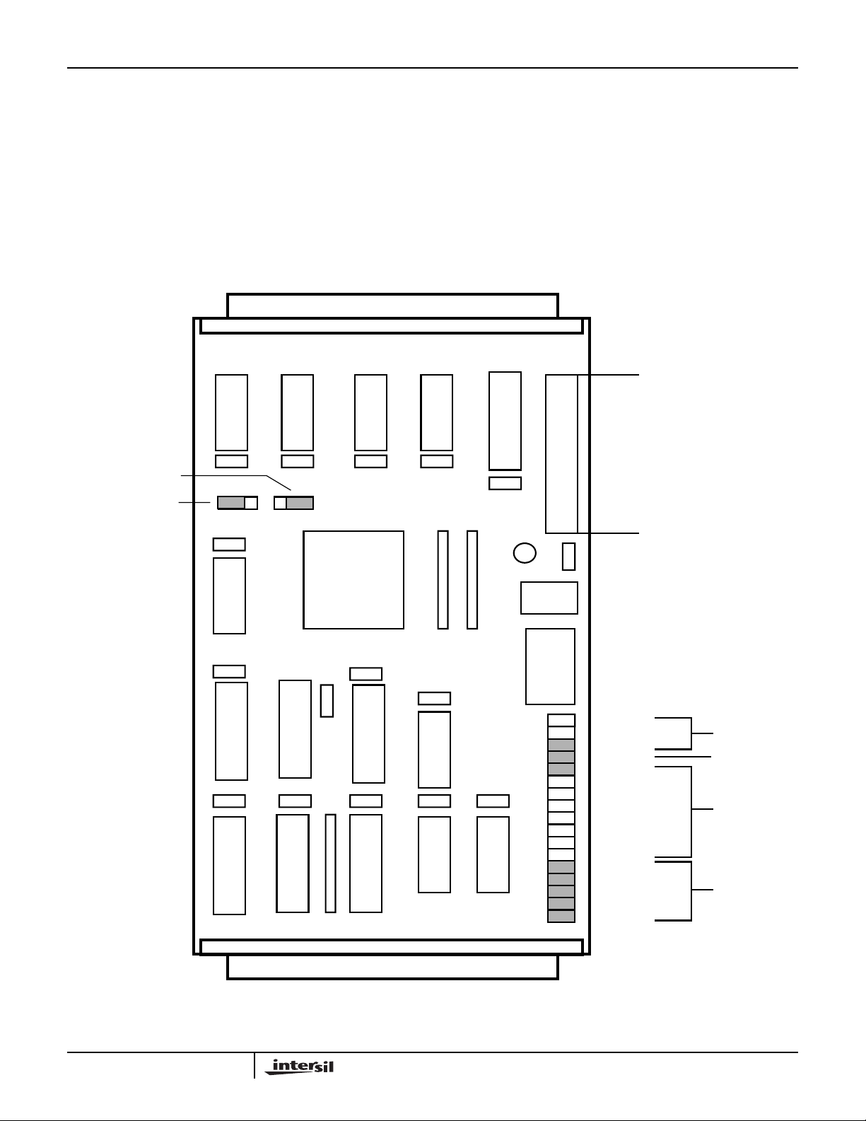
The HSP50016-EV was builtinto a 3U Euro-Card form factor
with dual 96 Pin Input/Output connectors. The I/O
connectors conform to the VME J2/P2 Connector Standard.
HSP50016 Evaluation Platform
1
CAUTION: These devices are sensitive to electrostatic discharge; follow proper IC Handling Procedures.
http://www.intersil.com or 407-727-9207
| Copyright © Intersil Corporation 1999

HSP50016-EV
Getting Started
This section describes the initial evaluation system setup for
the HSP50016-EV evaluation board. The system setup
consists of the evaluation board, software installation, and
system test to verify proper operation of the board.
Assembly
As part of the initial assembly, the HSP50016-EV must be
provided with the default jumper configuration to ensure
proper operation with the system test software. Each board
leaving the factory is supplied with the default configuration
as shown in Figure 1.
Before using the board with the supplied software, power
must be supplied to the board, and the HSP50016-EV must
be connected to the parallel port of the PC.
❏ Power is provided to the board by connecting the wall
mount power supply provided to connector J2. As an
alternative, power may be supplied by a standard 5V ±5%
supply through the J3 header or the HSP50016-EV’s 96
Pin DIN connectors P1 or P2.
❏ The HSP50016-EV is connected to the target PC by
connecting the HSP50016-EV’s26 Pin connector J1 to the
PC’s parallel port using the supplied ribbon cable.
System Requirements for the Evaluation Board
Software
The PC system targeted to run the HSP50016-EV software
(DDC-SOFT) and interface with the evaluation board must
meet the following requirements:
❏ IBM PC/XT/AT, PS/2, or 100% compatible with a minimum
of 640K of random access memory (RAM) (DDC-SOFT
does not require extended memory)
❏ At least 250kB of free disk space on the hard disk
❏ DOS Version 3.0 or higher
❏ One parallel port with 27 Pin D-Sub connector
Software Installation
The distribution diskette contains a program called
INSTALL.EXE which installs the DDC-SOFT software onto
the target hard disk. Note: The steps in this section assume
you are installing DDC-SOFT from a diskette in drive A: onto
a hard drive C:. If a different configuration is used, substitute
the letter of the drive where the diskette is located for drive
A: Substitute the letter for the hard drive for drive C:.
To start the installation program:
Make sure computer is on and the DOS prompt is displayed.
❏ Type: C:<Enter>
Create a subdirectory to contain the DDC-SOFT Programs
by typing:
❏ MD \DDCSOFT <Enter>
Change current directory to the DDCSOFT directory
❏ CD \DDCSOFT <Enter>
Start the installation process by typing:
❏ A:INSTALL <Enter>
The INSTALLprogram downloadsthe DDC-SOFTprograms,
DDCCTRL and DDCCMD, to the DDCSOFT subdirectory on
the target hard drive. In addition, a subdirectory called
DDC_CHK is created into which files used to perform
functional verification are downloaded.
Modifications to AUTOEXEC.BAT
To run the DDC-SOFT programs, DOS must be able to find
the executable files. To ensure that DOS can always find the
DDC-SOFT executables, modify the search path to include
the location of the DDC-SOFT directory. For example, if the
DDC-SOFT programs are installed on drive C: in a
subdirectory called\DDCSOFT, add the following line to the
end of the existing Path command in the AUTOEXEC.BAT
file:
❏ ;C:\DDCSOFT
If your AUTOEXEC.BAT file does not contain a PATH
command, add the following command to the file:
PATH=C:\DDCSOFT
❏ Reboot the PC so that the search path changes will take
effect.
System Test
Test software is provided to verify operation of the
HSP50016-EV Board. Prior to performing the system test, it
is assumed that the evaluation board has been assembled
and configured as described above, power has been applied
to the board, and the 26 Pin Connector J1 on board the
HSP50016-EV has been connected to the parallelport of the
target PC via the supplied cable. The system test is initiated
by the following:
Change the current directory to that which contains the
software required for the system test by typing:
❏ CD C:\DDCSOFT\DDC_CHK <Enter>
Run the system test software by typing:
❏ DDCCHK <Enter>
The DDCCHK.EXE batch file makes use of the Command
Line Interface (see Command Line Interface Section) to
initialize the evaluation board, clock a data vector through
the HSP50016-EV, and store the output to a file. The output
file is then compared, using the DOS command COMP, to a
file containing a set of vectors generated by a properly
functioning board. If the TEST_IN.DAT and TEST.OUT.DAT
files match, the assembled board passes operational
verification.
2
HSP50016-EV
When a successful compare has been done, the software
message returned is:
- Comparing files TEST_OUT.DAT and CMPRFILE.DAT
- FC: No differences encountered
The most common causes of test failuresare incorrect board
jumper settings, incorrect comm port selection, or a
corrupted eval.cfg file. It is helpful to delete the file
TEST_OUT.DAT, prior to the test, to ensure that DDC.CHK
runs properly and that a new TEST_OUT.DAT file was
created.
IQSTB SELECT
QOUT SELECT
JP20
11
JP19
P2
NOTE: if the operating system precedes DOS 6.0, the
user should answer NO to the COMP command prompt
to compare additional files. DOS Version 6.0 and above
use a different file compare command, so this step is
not necessary. DDCCHK checks the version
automatically and executes the proper compare routine.
The DDCCHK system test assumes that the LPT1 printer port
is being used for communication with the HSP50016-EV. If
another printer port is used, the Command Line Interface,
DDCCMD, m ust be used to configure the software for using
the correct port (see DDCCMD’s PPC and PP# command).
J1
CABLE
P1
JP1
JP2
JP3
JP5
JP6
JP7
JP8
JP9
JP10
JP11
JP12
JP13
JP14
JP15
JP16
JP17
JP18
J3
J2
EXT_CLK
OSC_CLK
PC_CLK
DATA_OE
ADDR0
ADDR1
ADDR2
ADDR3
ADDR4
ADDR5
ADDR6
ADDR7
DDC_CLK_INV
OUT_CLK_INV
CLK_OUT
CLK_IN
TAP_SEL
CLOCK
SELECT
OUTPUT
ENABLE
BOARD
ADDRESS
CLOCK
SELECT
FIGURE 1. LAYOUT OF HSP50016-EV SHOWING DEFAULT JUMPER CONFIGURATION
3

HSP50016-EV
HSP50016-EV Control Panel Software
The HSP50016-EV Control Panel is a graphical user
interface for controlling the operation of the HSP50016-EV
Board via an IBM PC or compatible. The control panel,
shown in Figure 3, supports loading the HSP50016's control
words; setting the state of control inputs; and specifying files
which serve as the sources and destinations for the
HSP50016's data and TAP inputs and outputs. Operation of
the control panel software is dependent on the clock source
provided to the HSP50016-EV as specified in the clock
select portion of the control panel. The HSP50016-EV
Control Panel is invoked by typing:
DDCCTRL <Enter>
Port Configuration
Communication between the Control Panel software and the
evaluationboard requires that the software knows which one
of the PC's parallel ports is being used for communication
with the HSP50016-EV and which board address the
HSP50016-EV has been configured for. The default
configuration assumes that LPT1 is being used and that the
HSP50016-EV has been configured for a board address of
0. The Port Configuration can be inspected by opening up
the port configuration window using the F9 function key. As
shown in Figure 4, the window displays the availableparallel
ports and their addresses. Also displayed are the current
port and HSP50016-EV board address being used by the
Control Panel software.
The current port and HSP50016-EV address are changed by
opening up the Port Configuration Window, using the
up/down arrow keys to select the desired parameter, and
toggling the space bar to change the selection. Proper
operation of the control panel software requires that the
HSP50016-EV board address specified in the port
configuration window matches the address jumpered in the
Address Selection Section of the HSP50016-EV’s headers
JP6-13.
Clock Select
The Clock Select portion of the control panel is used to tell
the Control Panel software which of four different clock
sources is being supplied to the HSP50016-EV. The choices
include one of two different software generated clocks
(Manual CLK or Port CLK), an oscillator clock provided by
the HSP50016-EV (Oscillator CLK), or an externally
supplied clock (External CLK). The clock mode selected
must be consistent with the Clock Select jumper position in
the HSP50016-EV’s headers JP1-3. If either Manual CLK or
Port CLK are specified in the Control Panel, the clock select
jumper must be inserted in JP3. If either Oscillator CLK or
External CLK is specified, the jumper must be inserted in
JP2 or JP1 respectively.
In Manual CLK mode, single clock pulses are sent to the
HSP50016 by depressing the F2 function key .The clock pulse
is software generatedby setting and clearing the PCCLK bit of
the Control Register U16 on the HSP50016-EV. After each
clock the HSP50016-EV's data outputs are inspected to see if
theyare ready to be read. If so, the data is read into the PC for
displayin the Control Panel. In this mode, file input and output
are supported (See File I/O Select Section).
In Port CLK mode, a free running clock is sent to the
HSP50016. The clock is started and stopped by depressing
the F2 function key. The clock pulses are software generated
by continually setting and clearing the PCCLK bit of Control
Register U16. After each clock the HSP50016-EV's data
outputs are inspected to see if they are ready to be read. If
so, the data is read into the PC for display in the Control
Panel. In this mode, file input and output are supported (see
File I/O Select Section).
In Oscillator CLK mode, the HSP50016 is supplied with a
clock by the oscillator on board the HSP50016-EV. In this
mode, the Control Panel can be used for modifying
and
IQSTRT, the control words, and the data and TAPinputs
to the DDC. However, the software is unable to provide file
based I/O to the evaluation board since the data rate
provided by the oscillator is much greater than that possible
through the parallel port of the PC. As a result, the Control
Panel disables file based I/O and the display of DDC output
in this mode.
Operation in External CLK mode is identical to that in
Oscillator CLK mode, except that the HSP50016 is supplied
with a clock through the 96 Pin DIN connector P1 on the
HSP50016-EV. Because this clock is asynchronous to the
PC, file based I/O and the DDC output displays are disabled.
The clocking mode used by the control panel is indicated by
the position of the “check mark” symbol within the Clock
Select portion of the Control Panel. A different clocking
mode may be selected by positioning the “check mark”
symbol in front of the desired clocking mode. The position of
the “check mark” is changed by using the cursor keys to
move the active window to the desired position and then
toggling the space bar to move the “check mark”.
RESET
File I/O Select
The File I/O Select portion of the Control Panel allows the
user to specify files which can be used as an input data
source or an output data destination for the HSP50016-EV.
The input data is loaded on to the input bus prior to the
software generated clock and the output data is read from
the output bus following the software generated clock.
If file based input is selected, the Control Panel software
down loads data from the specified file to registers on the
HSP50016-EV and clocks the data into the DATA0-15inputs
of the DDC. The Loop Count allows the user to simulate long
data streams by repeatedly sending the same input file.
If file based output is specified, the software reads the data
on the I and Q outputs of the HSP50016 and stores the data
in the specified file. The software automatically reads the
4

HSP50016-EV
output data and writes it into the output file as two’s
complement complex or real data. The configuration of the I,
Q, IQCLK and IQSTB pins is transparent to the user,
provided that none of the pins are three-stated and the DDC
Control Word fields Real Output, HDF Decimation Rate,
Number of Output Bits, I followed by Q and IQCLK rate are
compatible with each other. All valid output modes are
supported.
File based I/O is activated by using the space bar to toggle
the “check mark” symbol in the window proceeding the input
and output file identifiers in the control panel's file I/O
Section. If either file input or output is activated, the
respective file name must be entered in the window to the
right of the file identifier.File input or output may be disabled
at any time by toggling the respective “check mark”.
Note: File I/O is only valid when either the ‘Manual CLK’
or ‘Port CLK’ clocking modes are selected and it is
disabled if other clocking modes are specified.
Input and output data files are ASCII files whose format is
described in Appendix A. There is no limitation to the input
and output file size. Care must be taken if file output is
specified since data is collected in the file until file output is
deactivated or the DDCCTRL Program is exited.
TAP I/O files are similar, except that the TAP is available
regardless of the CLK setting. The format for the TAP input
and output files is given in Appendix B.
HSP50016 Data Inputs
The data window to the left of the HSP50016 icon is used to
specify hexadecimal values which drive the DDC's data
inputs DATA0-15. Data is entered into this window in
hexadecimal format starting with the most significant digit.
The contents of a particular data window may be edited by
following the window editing instructions in Appendix C.
If file input is selected, the data input is driven with data from
the specified file. On each clock the data window is updated
with the data sample down loaded from the file. In this mode
the data input window may not be manually updated.
HSP50016 Data I&Q Outputs
There are 32 bits available at P2. The control software for
the evaluation board performs a serial read via the PC Port.
Control Signals
The control signal portion of the control panel is used to
define the state of the DDC control signals
IQSTRT. The logical state of a control signal is set by using
the space bar to toggle the signal state in the window
preceding the specified control signal. When the evaluation
board is in Port CLK mode and
high, the DDC is automatically clocked five times. See the
HSP50016 Data Sheet for a complete description of the
control signals.
once after power up. The software DOES NOT do this
automatically.
RESET must be toggled low and high
RESET is set either low or
RESET and
Control Words
In the lower left hand corner of the control panel is a data
window which contains the hexadecimal values loaded into
the HSP50016's eight control words. The contents of a
particular control word may be updated by movingthe cursor
to the data window which is to be modified, selecting the
control word by pressing the space bar (which moves the
check mark to the desired control word) and depressing the
F4 key. A submenu pops up which parses that control word
into its various fields so that they may be examined or
modified individually.
The value entered into the data window is down loaded to
the HSP50016 and the submenu disappears when the user
depresses the F2 key. Leaving the window via the <Esc> key
ignores any changes made and returns to the main control
panel screen. If the update bit has been set, the new values
will update the configuration of the DDC and this will be
reflected in the submenu screen.
Note that all values displayed in this window are the last
values written to the control words, as opposed to
having been read from the DDC itself.
Help
Help windows are provided as a source of information for
control panel usage. The help window is activated by the F1
function key, and contains information based on the window
which is currently active.
Command Line Interface
As an alternative to the control panel, a command line
interface is provided which allows the user to control the
HSP50016-EV by issuing commands from the DOS prompt.
The commands perform basic I/O and configuration
functions by up or down loading data to the HSP50016
through the HSP50016-EV. The Command Line Program
has the following usage:
DDCCMD [Command] [ARG 1] [ARG 2] [ARG 3]
The Command specifies the action to be taken, and the
Arguments (ARG1, ARG2) represent additional data
required by the command. For example, to load Control
Word 1 with a value of 200000005(HEX) and set the update
bit, the user would type:
DDCCMD WCW 1 1 200000005 <Enter>
A summary of the command set is given in Table 2.
When several commands are to be entered consecutively,
the user may initiate the interactive command mode by
entering:
DDCCMD <Enter>
All commands are then entered as before, except that
control does not return to DOS between commands, and it is
not necessary to enter DDCCMD for each command. Note
5
HSP50016-EV
that the software automatically updates the control words
from the EVAL.CFG file upon entering the interactive mode.
Leaving the interactive mode is accomplished by typing
“quit” or “exit.”
DDCCMD gives the user the ability to control the evaluation
board via DOS batch files or system calls from a
programming language. The DDC_CHK6.BAT file discussed
in the System Test Section is an example of how the
Command Line Program might be used in a DOS batch file.
Configuration Jumpers
The Configuration Jumpers consists of the jumper headers
JP1-3 and JP5-20 as shown in Figure 1 and Table 1. Refer to
the evaluation board schematic found in the Appendices.
Most of these are self-explanatory, but the following bear
further discussion.
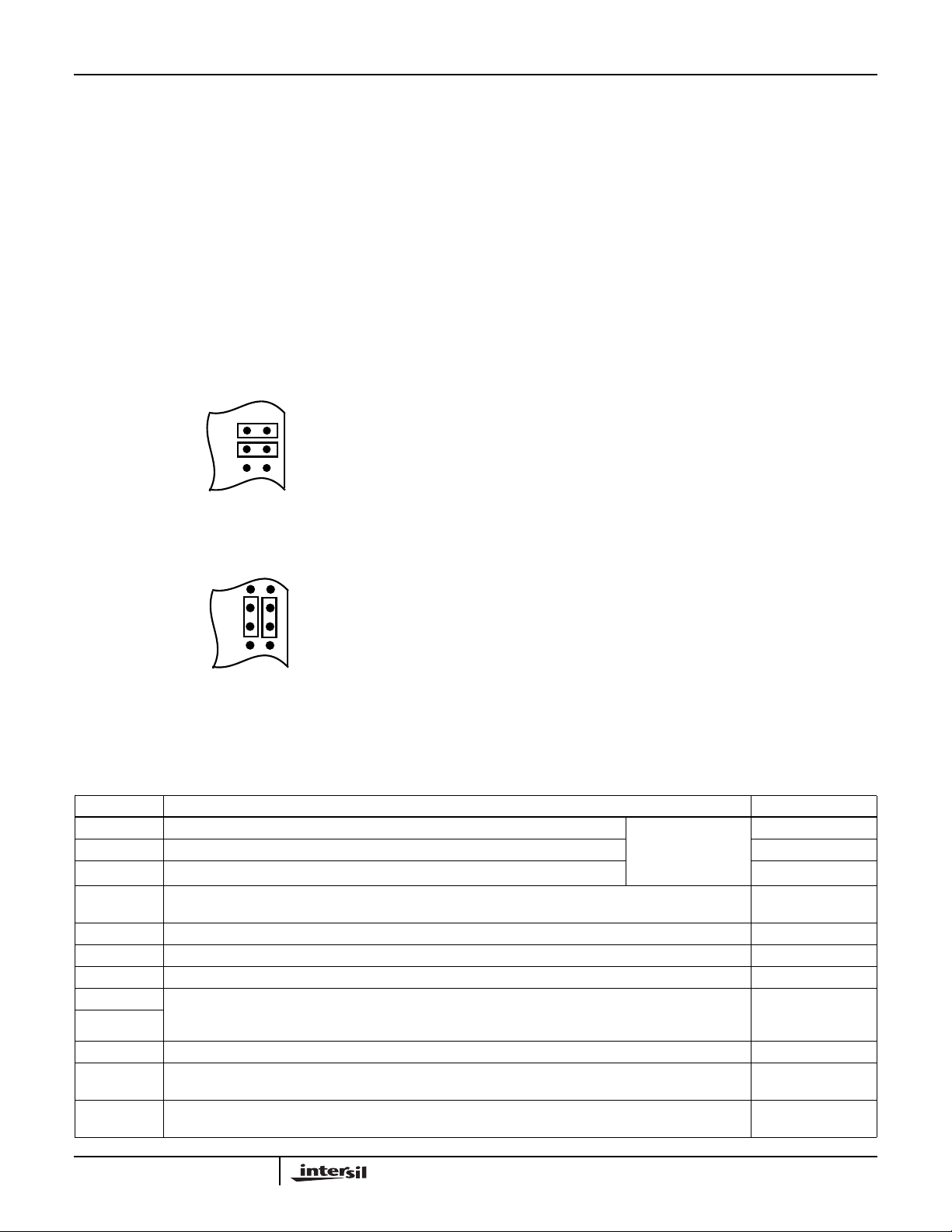
JP16
JP17
JP18
FIGURE 2. JUMPER CONFIGURATION IF CLOCK IS
SUPPLIED THROUGH P1 INPUT HEADER
JP15
JP16
JP17
JP18
FIGURE 3. JUMPER CONFIGURATION IF CLOCK IS
SUPPLIED THROUGH P2 OUTPUT HEADER
The jumpers JP16 and JP17 are used to select whether the
HSP50016's clock source is provided through the P1
connector or the P2 connector. If jumpers are inserted as
shown in Figure 2, a clock signal supplied through the
CLK_IN pin of the P1 input header drives a buffer whose
output clocks the HSP50016. The jumper inserted on JP16
feedsthe bufferedclock signal to the CLK_OUT pin of the P2
connector. If jumpers are inserted as shown in Figure 3, the
CLK_OUT pin of the P2 connector drives the clock buffer
which in turn drives the clock input of the HSP50016. The
jumper inserted between JP16 pin 2 and JP17 pin 2 allows
the CLKIN pin to be driven by the buffer output. NOTE: The
jumper placement shown in Figure 2 is the standard
configuration.
It is possible to configure the DDC so that the I, Q, IQCLK
and IQSTB outputs are in a high impedance state. Except for
IQSTB, these pins are pulled up on the evaluation board so
that they will not float under these conditions. Since IQSTB
can be either active high or low, it must be capable of being
pulled either way. JP19 determines whether IQSTB is pulled
up or down when it is three-stated. This jumper should be
installed such that IQSTB is pulled to its inactive state.
Note: The position of JP20 comes into play only when
parallel output from P2 is desired.
The jumper should be placed between pins 1 and 2 when
the DDC is configured for I followed by Q mode; the jumper
should be from JP20-2 to JP20-3 when I and Q are output
separately. The HSP50016-EV is shipped from the factory
with the default jumper configuration shown in Figure 1 and
Table 1. For the supplied software to properly control
operation of the HSP50016, it is assumed that the jumpers
are as specified in the default configuration; of course, once
the user is familiar with the operation of the board, this
configuration may be modified as required. The system test
software, DDCCHK, must be run using the default
configuration.
TABLE 1. DESCRIPTION OF JUMPER CONNECTIONS
JP DESCRIPTION DEFAULT
1 DDC CLK driven from external source when this jumper is installed. Only one of
2 DDC CLK driven from on board oscillator when this jumper is installed. 3 DDC CLK driven from PC software when this jumper is installed. Installed
5 DDC DATA0-15 driven from PC software when installed, otherwise data is from external source. Must be
installed or DATA0-15 lines must be driven to avoid damage to DDC.
6-13 Selects evaluation board address. Only one of these jumpers should be installed at a time. JP6 Installed
14 Selects input clock as inverted. Installed = non-inverted. Installed
15 Selects output clock as inverted. Installed = non-inverted. Installed
16 Direct flow of input and output clocks. JP16-1 is shorted to JP16-2 and JP17-1 is shorted to JP17-2 for the
17
18 TAP inputs driven by PC (installed) or from P2 (not installed). Installed
19 IQSTB pulled up (JP19-1 shorted to JP19-2) or pulled down (JP19-2 to JP19-3). Must be installed (in ei-
20 Serial to parallel converters configured for up to 32-bit, I followed by Q (JP20-1 to JP20-2) or 16 bit, I and
DDC CLK to be driven by the PC, on board oscillator, or connector pin P1C-20. To drive CLK from P2C20, jumper JP16-1 to JP17-1 and JP16-2 to JP17-2. JP1 must be installed in this configuration.
ther position) to avoid damage to evaluation board.
Q output separately (JP20-2 to JP20-3).
JP1, JP2 and JP3
selected
at a time.
JP16-1 to JP16-2,
-
Installed
JP17-1 to JP17-2
JP19-1 to JP19-2
JP20-2 to JP20-3
6
 Loading...