Intersil Corporation HSP50016 Datasheet
HSP50016
Data Sheet February 1999 File Number
Digital Down Converter
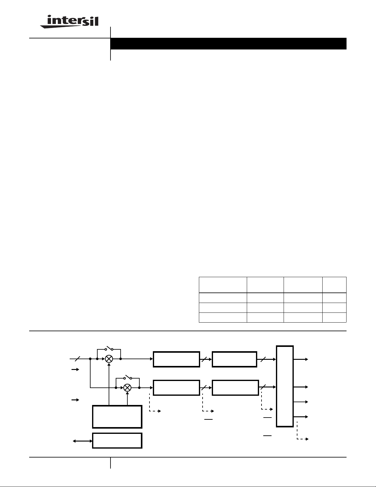
The Digital Down Converter (DDC) is a single chip
synthesizer, quadrature mixer and lowpass filter. Its input
data is a sampled data stream of up to 16 bits in width and
up to a 75 MSPS data rate. The DDC performs down
conversion, narrowbandlow pass filtering and decimation to
produce a baseband signal.
The internal synthesizer can produce a variety of signal
formats. They are: CW, frequency hopped, linear FM up
chirp, and linear FM down chirp. The complex result of the
modulation process is lowpass filtered and decimated with
identical real filters in the in-phase (I) and quadrature (Q)
processing chains.
Lowpass filtering is accomplished via a High Decimation
Filter (HDF) followed by a fixed Finite Impulse Response
(FIR) filter. The combined response of the two stage filter
results in a -3dB to -102dB shape factor of better than 1.5.
The stopband attenuation is greater than 106dB. The
composite passband ripple is less than 0.04dB. The
synthesizer and mixer can be bypassed so that the chip
operates as a single narrow band low pass filter.
The chip receives forty bit serial commands as a control
input. This interface is compatible with the serial I/O port
available on most microprocessors.
The output data can be configured in fixed point or single
precision floating point. The fixed point formats are 16,
24, 32, or 38-bit, two’s complement, signed magnitude, or
offset binary.
The circuit provides an IEEE 1149.1 Test Access Port.
3288.6
Features
• 75 MSPS Input Data Rate
• 16-Bit Data Input; Offset Binary or 2’s Complement
Format
• Spurious Free Dynamic Range Through Modulator
>102dB
• Frequency Selectivity: <0.006Hz
• Identical Lowpass Filters for I and Q
• Passband Ripple: <0.04dB
• Stopband Attenuation: >104dB
• Filter -3dB to -102dB Shape Factor: <1.5
• Decimation Factors from 32 to 131,072
• IEEE 1149.1 Test Access Port
• HSP50016-EV Evaluation Board Available
Applications
• Cellular Base Stations
• Smart Antennas
• Channelized Receivers
• Spectrum Analysis
• Related Products: HI5703, HI5746, HI5766 A/Ds
Ordering Information
PART
NUMBER
HSP50016JC-52 0 to 70 44 Ld PLCC N44.65
HSP50016JC-75 0 to 70 44 Ld PLCC N44.65
HSP50016GC-52 0 to 70 48 Ld CPGA G48.A
TEMP.RANGE
(oC) PACKAGE
PKG.
NO.
Block Diagram
16
DAT A
CLK
CONTROL
TEST ACCESS
PORT/CTRL
COS
GENERATOR
TEST ACCESS
3-198
COMPLEX
SINUSOID
PORT
SIN
HIGH DECIMATION
FILTER
HIGH DECIMATION
FILTER
CLK CLK
CAUTION: These devices are sensitive to electrostatic discharge; follow proper IC Handling Procedures.
http://www.intersil.com or 407-727-9207
LOW PASS FIR
FILTER
LOW PASS FIR
FILTER
R
I
Q
OUTPUT
FORMATTER
CLK
4R
OR
CLK
2R
| Copyright © Intersil Corporation 1999
I
OUTPUT
Q
IQSTRB
IQCLK
CLK
SER
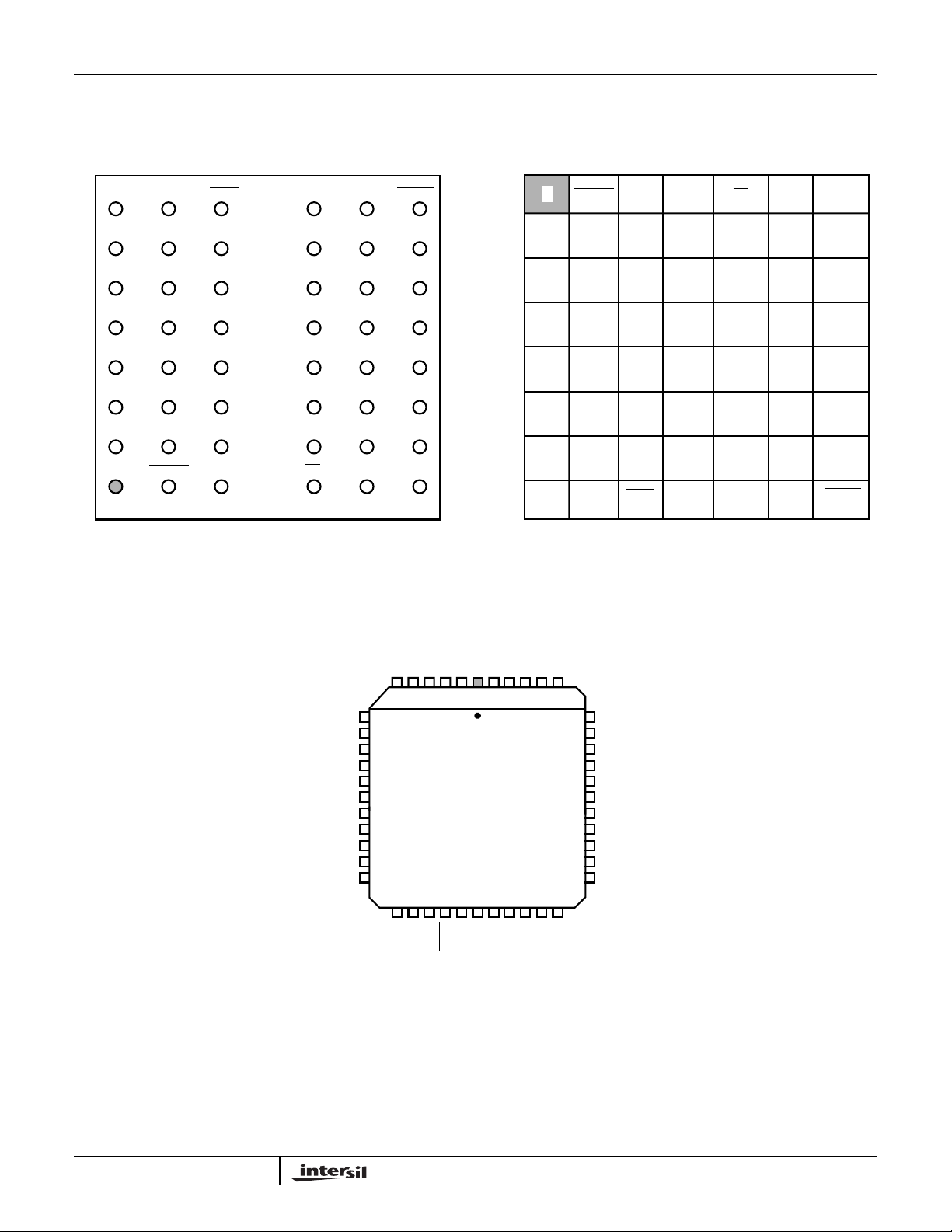
Pinouts
48 PIN CPGA
BOTTOM VIEW
HSP50016
48 PIN CPGA
TOP VIEW
123 678
CC
CC
TRST
GND
DAT A1
DAT A5
DAT A6
IQSTB
V
DAT A8 DAT A7
DAT A9
DATA14
DATA15
V
CS
CC
CC
V
CC
DATA11
DATA12
GND
V
CDATA
CC
TDI TDO
H
V
DAT A0
GND DATA2
DAT A3
V
GND
I
IQSTRT IQCLK
123 678
G
F
E
D
C
B
A
GND
CLK
V
CC
V
CC
DAT A4
Q
RESETTCK TMS
GND
DATA10
V
CC
GND
DATA13
CCLK
CSTB
44 LEAD PLCC
TOP VIEW
A
B
C
D
E
F
G
H
DAT A4
CLK
I
IQSTRT
Q
GND
V
V
DAT A3
CC
GND DATA2
V
CC
V
GND
TDI TDO
CC
CC
IQCLK
IQSTB
DAT A6
DAT A5
DAT A1DAT A0
GND
TRST
CS CSTB
CDATA
V
DATA15
DATA14
DAT A9
DAT A8 DATA7
V
CC
CC
V
CC
GND
DATA12
DATA11
V
CC
DATA10
CCLK
DATA13
GND
V
CC
GND
RESETTCK TMS
V
CC
DAT A6
DAT A5
DAT A4
DAT A3
V
CC
GND
CLK
DAT A2
DAT A1
DAT A0
7
8
9
10
11
12
13
14
15
16
17
GNDQI
CC
V
GND
IQSTB
IQCLK
20 21 22 23 24 25 261918
TDI
TRST
CDATA
IQSTRT
44 43 42 41 40
123456
CC
V
TDO
TMS
CS
TCK
CSTB
CCLK
2827
GND
RESET
CC
V
39
GND
38
DATA15
37
DATA14
36
DATA13
35
DATA12
34
GND
33
DATA11
32
DATA10
31
DAT A9
30
DAT A8
29
DAT A7
CC
V
3-199
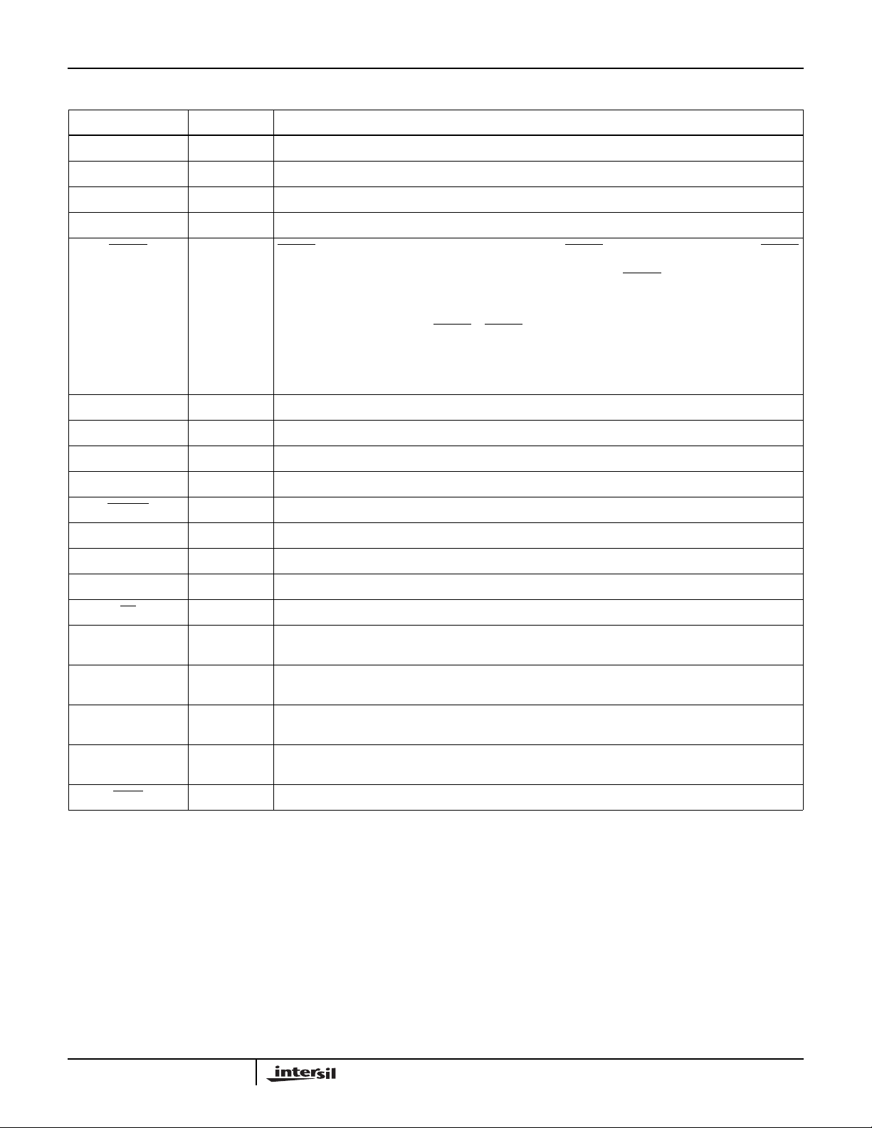
Pin Description
NAME TYPE DESCRIPTION
HSP50016
V
CC
GND - Ground.
DATA0-15 I Input Data Bus. Selectable between two's complement and offset binary. DATA0 is the LSB.
CLK I Clock for input data bus. fS is the frequency of CLK, which is also the input sample rate.
RESET I RESET initializes the internal state of the DDC. During RESET, all internal processing stops. RESET
I O The I output has three modes: I data; I data followed by Q data; real data.
Q O The Q output has two modes: Q data and the carry out of the Phase Adder.
IQCLK O IQ Clock: Bit or word clock for the I and Q outputs.
IQSTB O IQ Strobe: Beginning or end of word indicator for I and Q.
IQSTRT I IQ Start: Initiates output data sequence. Active low.
CDATA I Control Data: Port for control data input.
- +5V Power.
facilitates the synchronization of multiple chips for Auto Three-State operation. If the Force bits in Control
Word 7 are inactive and the IEEE Test Access Port is in an Idle state, RESET causes the IQCLK, IQSTB,
I and Q outputs to go to a high impedance state.
All Control Registers are updated from their respective Control Buffer Registers on the third rising edge
of CLK after the deassertion of RESET. If RESET is deasserted tRSnanoseconds prior to the rising edge
of CLK, the internal reset will deassert synchronously. If tRSis violated, then the circuit contains a synchronizer which will cause reset to be deasserted internally one or more clocks later.
An initial reset is required to guarantee proper operation of the DDC. Active low.
CCLK I Control Data Clock: Control data input bit clock.
CSTB I Control Data Strobe: Beginning of word indicator for control data.
CS I Chip Select: Enables control data loading of DDC. Active low.
TCK I Test Clock: Bit Clock for IEEE 1149.1 Data. This signal should be either tied low or pulled high when the
TAP is not used.
TMS I Test Port Mode Select: This signal should be either left unconnected or pulled high when the TAPisnot
used.
TDI I TestData Input for IEEE Test Port: This signal should be either left unconnected or pulled high when the
TAP is not used.
TDO O Test Data Output for IEEE Test Port: This output will be in the high impedance state when the TAP is
not used.
TRST I Test Port Reset. Active Low. This signal should be tied low when the TAP is not used.
3-200
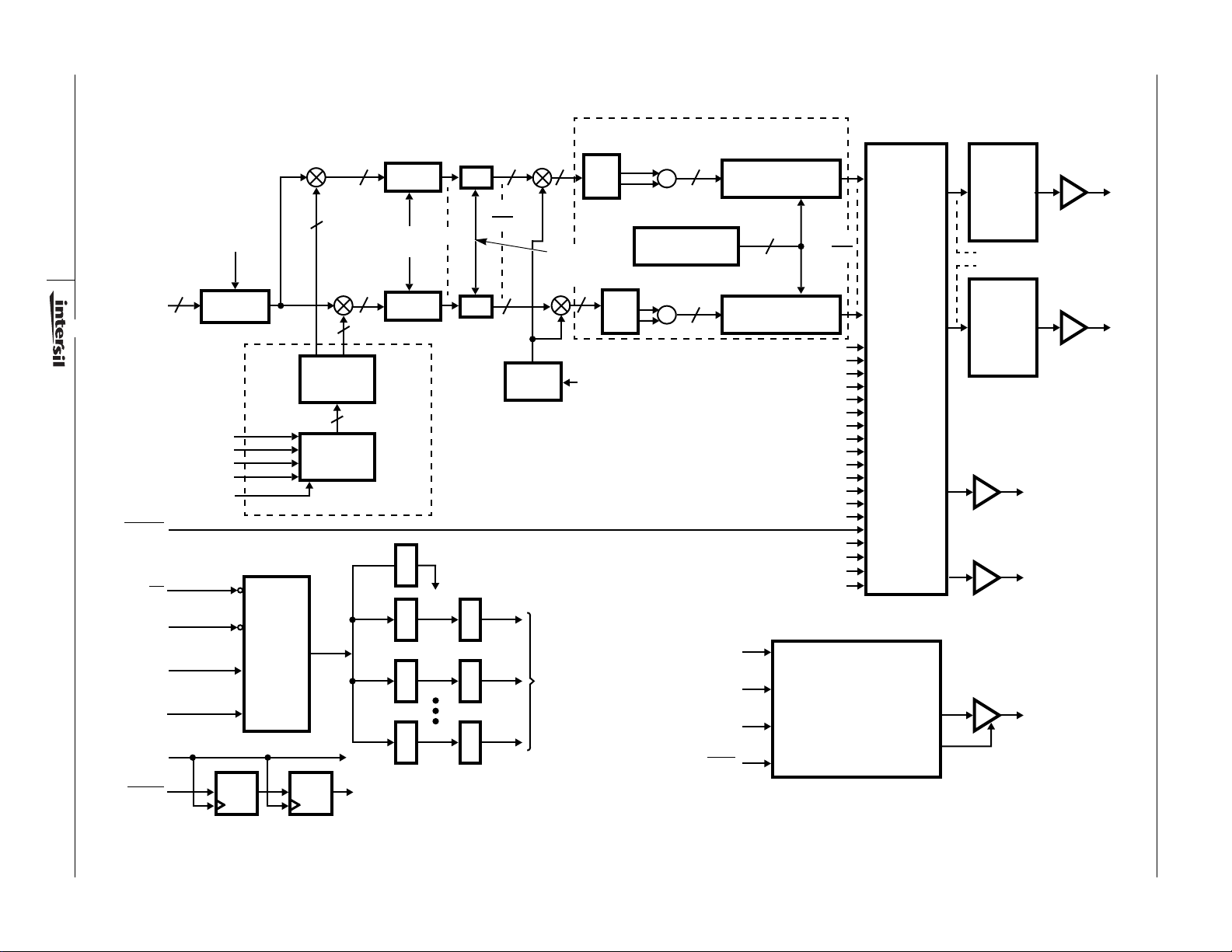
DDC Functional Block Diagram
3-201
DATA0-15
†
†
DELTA PHASE INCR
†
IQSTRT
16
MIN PHASE INCR
†
PHASE OFFSET
MAX PHASE INCR
†
MODE
CS
†
INPUT
FORMAT
INPUT
REGISTER
SECTION SECTION
COS
GENERATOR
PHASE WORD
GENERATOR
MIXER
SHIFTER
17
17
SIN
SIN/COS
18
PHASE
LOCAL OSCILLATOR
†
HDF
SHIFT
SHIFTER
17
17
0
CLK
HDF
HDF
HDF
SCALING
MULTIPLIER
18
CLK
R
18
SCALE
FACTOR
DAT A
RAM
17
COEFFICIENT
†
HDF
DECIMATION
COUNTER PRELOAD (DCP)
DAT A
17
RAM
†
SCALING
MULTIPLIER
GAIN
ROM
++
†
I POLARITY AND THREE-STATE CTRL
†
Q POLARITY AND THREE-STATE CTRL
†
TEST ENABLE AND CONTROL SIGNALS
FIR SECTION
MULTIPLIER/
ACCUMULATOR
18
22
MULTIPLIER/
ACCUMULATOR
18
†
WAIT FOR RAM FULL
†
OUTPUT FORMAT
†
TIME SLOT LENGTH
†
NUMBER OF OUTPUT BITS
†
†
IQSTRB THREE-STATE CTRL
†
OUTPUT SENSE
†
I FOLLOWED BY Q
†
TIME SLOT NUMBER
†
IQCLK POLARITY
†
IQCLK DUTY CYCLE
†
IQCLK DURATION
IQCLK THREE-STATE CTL
†
IQSTRB POLARITY
†
IQSTRB LOCATION
†
IQ CLK RATE
CLK
4R
FORMATTER
(P ARALLEL
TO SERIAL
CONVERTER
AND BUFFER)
SHIFT
REGISTER
CLK
SER
SHIFT
REGISTER
I
= IQCLK
Q
HSP50016
IQSTB
IQCLK
CSTB
CDATA
CCLK
CLK
RESET
DECODER
DQ DQ
1
2
7
CONTROL
BUFFERS
1
†
2
7
CONTROL
REGISTERS
CONTROL
P ARAMETERS
FIGURE 1. FUNCTIONAL BLOCK DIAGRAM
TCLK
TMS
TDI
TRST
IEEE 1149.1
TEST ACCESS PORT
† Indicates parameters from control registers.
TDO
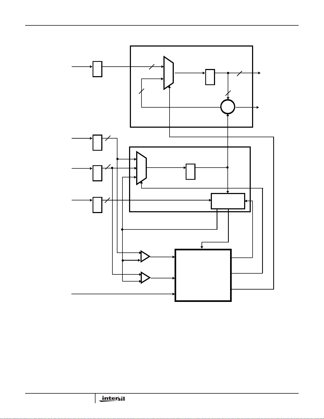
Phase Generator Block Diagram
HSP50016
PHASE ACCUMULATOR
†
PHASE OFFSET
†
MAXIMUM PHASE
INCREMENT
†
MINIMUM PHASE
INCREMENT
†
DELTA PHASE
INCREMENT
R
E
G
>
18
MUX
0 1
33
PHASE REGISTER
R
E
G
>
33
18
PHASE WORD
(TO THE
SIN/COS
GENERATOR)
+
+
PHASE ADDER
CARRY OUT
-
32
R
E
G
>
32
R
E
G
>
32
R
E
G
>
PHASE INCREMENT ACCUMULATOR
MUX
0 1 2
MUX SELECT 0
MUX SELECT 1
PHASE
INCREMENT
REGISTER
R
E
G
>
ADDER /
SUBTRACTOR
≤
>
†
MODE
CONTROL
† Indicates parameters set in Control Registers.
FIGURE 2. PHASE GENERATOR BLOCK DIAGRAM
Functional Description
The primary function of the DDC is to extract a narrow
frequency band of interest from a wideband input, convert that
band to baseband and output it in either a quadrature or real
form. This narrow band extraction is accomplished b y do wn
converting and centering the band of interest at DC. The
conversion is done by m ultiplying the input data with a
quadrature sinusoid. A quadrature lowpass filter is applied to
INITIALIZE
PHASE INCR.
TO MIN
INITIALIZE
PHASE INCR.
TO MAX
CARRY OUT
ADD/SUBTRACT
MUX SELECT 0
CONTROL
MUX SELECT 1
the multiplier outputs. Identical real lowpass filters are
provided in the in-phase (I) and quadrature phase (Q)
processing branches. Each filtering chain consists of a
cascaded HDF and FIR filter, which e xtr acts the band of
interest. During filtering, the signal is decimated by a rate
which is proportional to the output bandwidth. The bandwidth
of the resulting signal is the double sided passband width of
the lowpass filters. An Output Formatter manipulates the filter
output to provide the data in a variety of serial data formats.
3-202
HSP50016
Local Oscillator
Signal data clocked into the DATA0-15 input of the DDC is
multiplied by a quadrature sinusoid in the Mixer Section (see
Figure 1). The data input to the DDC is a 16-bit real data
stream which is sampled on the rising edges of CLK. It can
be in two's complement or offset binary format.
The input data is passed to a mixer, which is composed of
two real multipliers. One of these multiplies the input data
samples by the in-phase (cosine) component of the
quadrature sinusoid, and the other multiplies the input data
samples by the quadrature (sine) component. The in-phase
and quadrature data paths are designated I and Q
respectively. The sine and cosine are generated in the local
oscillator as shown in Figure 1.
The local oscillator is programmed to produce a quadrature
sinusoid with programmable frequency and phase. The
frequency can be constant (Continuous Wave-CW), linearly
increasing (up chirp), linearly decreasing (down chirp), or
linear up/down chirp. The initial phase of the waveform is set
by the phase offset.
The phase, frequency and chirp limits of the quadrature
sinusoid are controlled by the Phase Generator (Figure 2).
The output of the Phase Generator is an 18-bit phase word
that represents the current phase angle of the complex
sinusoid. The Phase Generator automatically increments the
phase angle by a preprogrammed amount on every rising
edge of CLK. Stepping the output phase from 0 through full
scale (2
sinusoid from 0 to (-2+2
stepped in a clockwise (decreasing) direction to support
down conversion.
determined by the number of clocks needed for the phase to
step though its full range of 2π radians. The required phase
increment for a given local oscillator frequency is calculated by:
where:
f
fS is the input sampling frequency
Phase Increment is the Control Word Value (in Hex)
There are five parameters which control the Phase Generator:
Phase offset, minimum phase increment, maximum phase
increment, delta phase increment and Mode Control. These
values are programmed via Control Words 2, 3, and 4. Mode
Control is used to select the function of the other parameters.
The phase offset is the initial setting of the phase word going
to the SIN/COS Generator. Subsequent phases of the
sinusoid are calculated relative to this offset. The minimum
phase increment has two mode dependent functions: when
the SIN/COS Generator is forming a CW waveform, the
18
- 1) steps the phase angle of the quadrature
-17
)π radians.
The frequency of the complex sinusoid is
Phase Increment INT fCfS⁄()2
f
Phase Incr()fS2
C
is the desired local oscillator frequency
C
=
33–
[]H
; 0 fCfS/2<<=
33
NOTE: The phase is
(EQ. 1)
minimum phase increment is the phase step taken on every
clock. When the SIN/COS Generator is producing a chirped
sinusoid, the minimum phase increment is the smallest
phase step taken. Maximum phase increment is only used
during Chirped Modes; it is the largest allowable phase
increment. During Chirp Modes, the delta phase increment
is the difference between successive phase increments.
The four phase parameters are stored in their respective
registers in the Phase Generator. The Phase Register stores
the current phase angle. On the first clock following the
deassertion of
RESET, the 18 MSBs of the Phase Register
are loaded from the Phase Offset Register. On every rising
edge of CLK thereafter, the output of the Phase Increment
Register is subtracted from the 32 LSBs of the current
phase. The 33-bit difference is stored back in the Phase
Register on the next CLK. The 18 most significant bits of the
Phase Register form the phase word, which is the input to
the SIN/COS Generator.
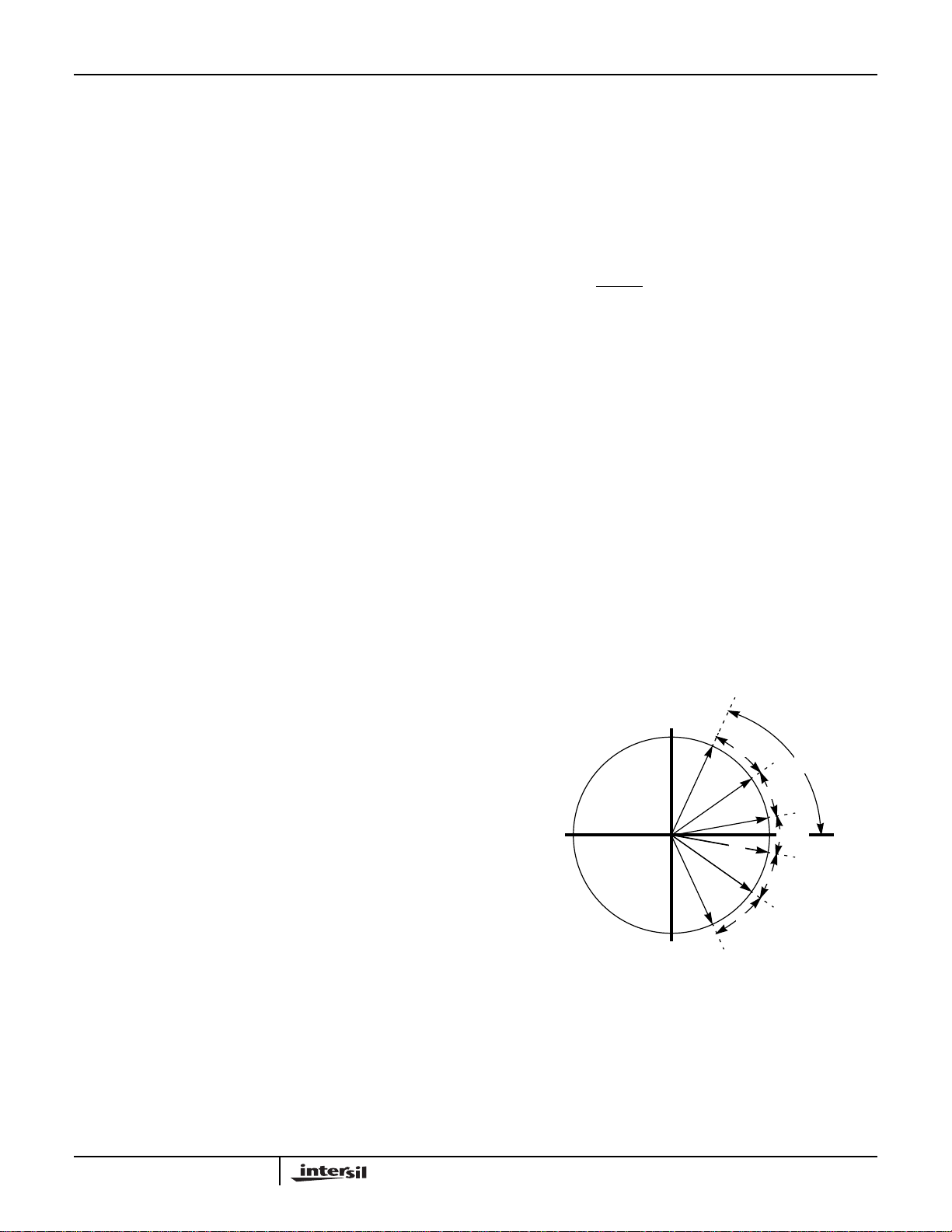
Figure 3 gives a graphic representation of the phase
parameters for the CW case. To understand their
interrelationships, the phase should be visualized as the
angle of a rotating vector. When the local oscillator in the
DDC is programmed to generate a CW waveform, the
multiplexers are configured so that the Minimum Phase
Increment is stored in the Phase Increment Register; this
value is subtracted from the output of the Phase Register on
every CLK and the difference becomes the new Phase
Register value. The Delta Phase Increment and Maximum
Phase Increment are ignored when generating a CW.
STARTING PHASE
o
+90
θ
INCR
(0)
(1)
(5)
(4)
(2)
(3)
θ
INCR
o
±180
o
-90
FIGURE 3. PHASE WORD PARAMETERS FOR CW CASE
θ
θ
INCR
θ
INCR
INCR
θ
OFFSET
o
0
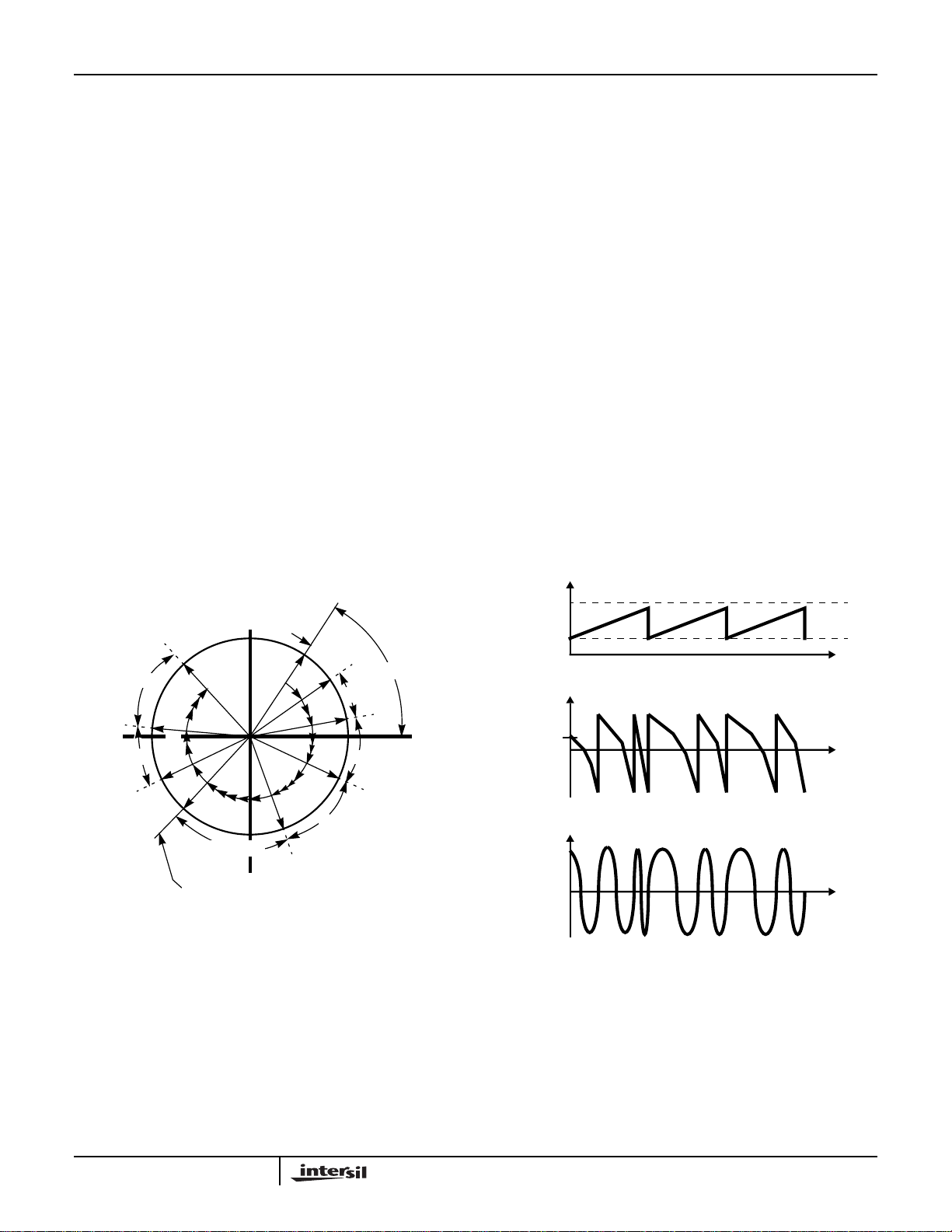
In Up Chirp Mode the local oscillator generates a signal
with a linearly increasing frequency (Figure 4A). The Phase
Increment Register is initially loaded with the minimum
Phase Increment value; on every clock, the contents of the
Phase Increment Register is subtracted from the current
output of the Phase Register. Simultaneously, the Delta
3-203
HSP50016
Phase Increment Register is added to the 24 LSBs of the
output of the Phase Increment Register. On the next CLK,
that sum is stored back in the Phase Increment Register,
the new phase is stored in the Phase Register and the
process is repeated. The phase increment is allowed to
grow until the next phase increment would equal or exceed
the maximum phase increment value. When this happens,
the Phase Increment Register is reset to the minimum
phase increment and the cycle starts over again.
NOTE: The phase increment is never equal to the
maximum phase increment, since the Phase Increment
Register is reloaded if the next phase increment value
would be greater than the maximum phase increment.
From the time the Phase Generator starts at the minimum
phase increment until it reaches the maximum phase
increment, the phase word on clock n is given by:
Phase Word Phase Offset - Minimum Phase Increment
=
[
n (Delta Phase Increment)+
(EQ. 2)
]
An example of the outputs of the Phase Increment Register,
Phase Register, and the I output of the SIN/COS Generator
are shown in Figure 4B.
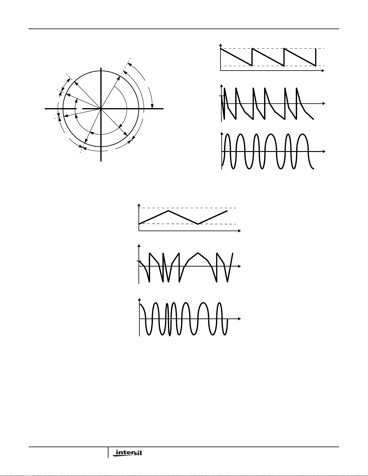
In Down Chirp Mode the local oscillator generates a signal
with a linearly decreasing frequency (Figure 5A). The
maximum phase increment is loaded into the Phase
Increment Register and the phase offset value goes into
the Phase Register. The delta phase increment is
subtracted from the 24 LSBs of the phase increment to
form a new phase increment at each clock. The phase
increment is allowed to diminish until it reaches the
minimum phase increment value, then it is reset to the
maximum phase increment value and the cycle is repeated.
Note that the value of the phase increment can be equal to,
but never less than the minimum phase increment, since
the Phase Increment Register is reloaded if the next phase
increment value would be less than the minimum phase
increment. This feature protects the DDC from exceeding
the Nyquist frequency.In this case, from the time the Phase
Generator starts at the maximum phase increment until it
reaches the minimum phase increment, the phase word on
clock n is given by:
Phase Word Phase Offset -[Minimum Phase Increment
=
n (Delta Phase Increment)]–
(EQ. 3)
See Figure 5B for a graphical representation of this process.
PHASE INCREMENT
θ
±180
θ
INCR+θ∆
INCR
o
+2θ
θ
∆
(7)
(6)
INCR
IF
θ
INCR
THEN
START NEW RAMP
(8)
(5)
θ
+90
+4θ
INCR
+5θ∆ > θ
-90
o
∆
o
(0)
(4)
MAX INCR
STARTING PHASE
θ
INCR
(1)
(2)
(3)
θ
INCR
θ
INCR+θ∆
θ
INCR
+3θ
∆
θ
OFFSET
+2θ
o
0
∆
MAXIMUM
MINIMUM
PHASE WORD
PHASE
OFFSET
COSINE OUTPUT OF SIN/COS GENERATOR
FIGURE 4A. PHASE WORD DURING UP CHIRP FIGURE 4B. UP CHIRP
TIME
TIME
TIME
3-204
HSP50016
PHASE INCREMENT
STARTING PHASE
o
+90
θ
MAX INCR
-4θ
±180
θ
MAX INCR
-3θ
o
θ
∆
∆
MAX INCR
-2θ
∆
(5)
(4)
(3)
(2)
-90
(0)
o
(1)
θ
MAX INCR
-θ
∆
FIGURE 5A. PHASE WORD DURING DOWN CHIRP
PHASE INCREMENT
MAXIMUM
MINIMUM
θ
OFFSET
θ
MAX INCR
MAXIMUM
MINIMUM
PHASE WORD
PHASE
OFFSET
o
0
COSINE OUTPUT OF SIN/COS GENERATOR
TIME
TIME
TIME
FIGURE 5B. DOWN CHIRP
TIME
PHASE WORD
PHASE
OFFSET
COSINE OUTPUT OF SIN/COS GENERATOR
FIGURE 6. UP/DOWN CHIRP
In Up/down Chirp Mode, the phase accumulator is set to the
phase offset value and the minimum phase increment is
loaded into the Phase Increment Register. The delta phase
increment is added to the 24 LSBs of the Phase Increment
Register to form a new phase increment at each clock. The
phase increment is allowed to grow until it nears the
maximum phase increment value (as defined in the up chirp
description). The delta phase increment value is then
subtracted from the least significant bits of the Phase
Increment Register to form a new phase increment at each
clock. The phase increment is allowed to diminish until it
TIME
TIME
reaches the minimum phase increment value (as defined in
the down chirp description). The Phase Increment Register
is then reloaded with the minimum phase increment, and the
up/down cycle begins again. See Figure 6 for a graphical
representation of this process.
The minimum and maximum phase increments have
allowable values from 0 to 2
32
-1. This corresponds to the
phase increment:
0 Phase Increment π 12
–()radians<<
32–
(EQ. 4)
3-205
HSP50016
The Delta Phase Increment parameter can take on values
from 0 to 2
24
- 1 which corresponds to the Delta Phase
Increment:
0 DeltaPhase Increment π 28–2
–()radians<<
32–
(EQ. 5)
The output of the phase accumulator forms the input to the
SIN/COS Generator which in turn produces a quadrature
vector which rotates clockwise: the outputs are cos(ωn) and
-sin(ωn). The outputs of the SIN/COS Generator are two's
complement values which are scaled to prevent overflow in
subsequent operations in the DDC under normal operation.
The scale factor has a negligible effect on the end to end
DDC gain.
The frequency resolution of the DDC = (frequency of CLK)/
(Number of Phase Register bits). At the maximum clock rate,
this results in a frequency selectivity of 75MHz/2
33
= 0.009Hz.
The 18-bit phase word yields a phase noise figure of greater
than 102dB.
Mixer
The Mixer performs quadrature modulation by multiplying
the output of the SIN/COS Generator by the input data. The
outputs of the I and Q multipliers are symmetrically rounded
to 17 bits to preserve the 102dB spurious free dynamic
range (SFDR). The result of the quadrature modulation
process is passed to the High Decimating Filter (HDF)
Section.
the input data to the HDF for the maximum dynamic range
while avoiding overflow errors. The shift factor is
programmed into the Shift field of Control Word 4. The value
in this field is calculated by the equation:
Shift 75 Ceiling 5 log
R()()–=
2
(EQ. 7)
where R is the HDF decimation factor and Ceiling(X)
denotes the ceiling function of X; i.e., the result is X if X is an
integer, otherwise the result is the next higher integer.
During
RESET, the HDF is initialized and will not output any
information until it is filled with new data.
NOTE: The output rate of the HDF is CLK divided by the
HDF decimation factor (CLK/R).
The HDF decimation
counter preload (DCP) is programmed in Control Word 5,
bits 21-35 and has the value: DCP = R -I, where R is the
HDF decimation factor.
0
-20
-40
-60
GAIN (dB)
-80
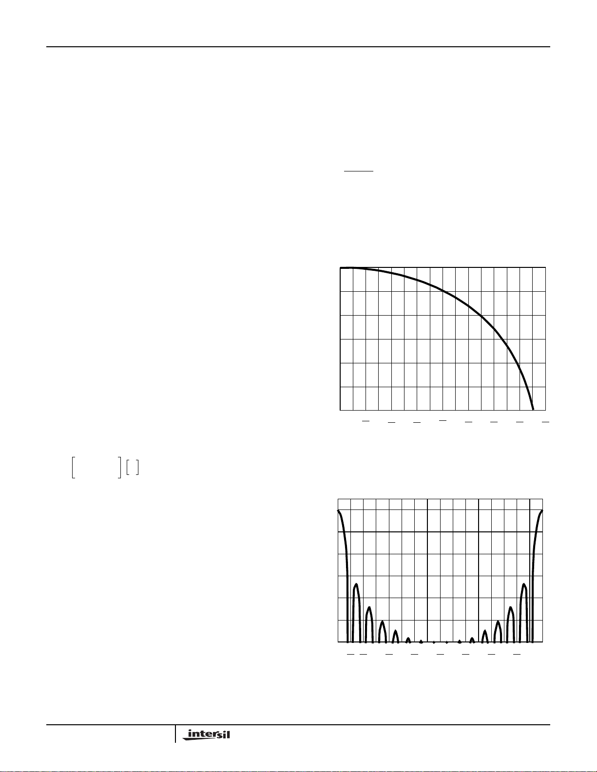
High Decimation Filter
The High Decimation Filter (HDF) Section is comprised of
two real HDF filters, one processing the I data branch and
one processing the Q data branch. Each branch has the
lowpass response shown in Figure 7. The normalized HDF
frequency impulse response is given by the equation:
5
Sin πFS()
--------------------------------
Hf()
=
where F
Sin πF
/R()
S
is the input sampling rate; R is the decimation
S
(rate change) factor.
Figure 7A shows this equation plotted from DC to the first
null, while Figure 7B shows the equation plotted from DC
response to f
.
S
NOTE: The HDF is a true FIR filter; i.e., the phase is linear.
The data path through the HDF was designed to ensure a
true 16-bit noise floor (approximately 98dB) at the output of
the DDC. The structure of the HDF filter used in the DDC is a
five stage decimation filter. The width of each successive
stage decreases such that the LSBs are lost due to
truncation [1]. As a result, the data must be processed in the
MSBs of the filter so that the noise due to truncation is below
the required noise floor. Thus, the input data of the HDF
must be shifted so that its output data fills the HDF output
word. The shift is a function of the desired HDF decimation
rate R and the number of HDF filter stages (which is fixed at
5). The shift is performed by the Data Shifter,which positions
5
I
--- -
R
(EQ. 6)
-100
-120
f
8R
f
S
S
4R
f
3f
S
S
2R
8R
FREQUENCY (Hz)
5f
8R
7f
3f
S
4R
S
S
8R
FIGURE 7A. FREQUENCY RESPONSE OF HIGH DECIMATION
FILTER FROM DC TO FIRST NULL
(FOR R = 16)
Gain (dB) = 20log [H(f)]
0
-20
-40
-60
GAIN (dB)
-80
-100
-120
f
S
R
S
S
R
R
S
S
2
R
FREQUENCY (Hz)
S
R
10f
f
6f
4f
2f
12f
14f
S
S
R
R
FIGURE 7B. DDC HC FREQUENCY RESPONSE
(FOR R = 16)
Gain (dB) = 20log[H(f)]
f
S
R
f
S
3-206
HSP50016
Scaling Multipliers
The output of each HDF is passed to a Scaling Multiplier.
The Scaling Multipliers are used to compensate for the HDF
gain, which is between 1 (inclusive) and 0.5 (non-inclusive),
or (0.5, 1.0). The gain through the HDF is dependent on the
decimation factor: when the decimation is an even power of
two, the HDF gain is equal to 1; otherwise, the gain must be
compensated for in the Scaling Multiplier. The HDF gain is
given by the equation:
HDF Gain R5/2
CEILING 5 log2R()()
=
where R is the HDF decimation factor. The compensating
Scale Factor, which is input to both Scaling Multipliers, is
given by the equation:
Scale Factor 2
CEILING 5 log2R()()
R5⁄=
where R is the HDF decimation factor.
NOTE: The Scale Factor falls in the interval [1, 2).
output of the scaling multiplier is symmetrically rounded to
17 bits.
(EQ. 8)
(EQ. 9)
The
The binary formats of the inputs and outputs of the scaling
multiplier are as follows:
Input from HDF: a
Scale factor: a
Output: a
(-20). a1(2-1) a2(2-2)... a17(2
0
(20). a1(2-1) a2(2-2)... a15(2
0
(-20). a1(2-1) a2(2-2)... a16(2
0
-17
-15
-16
FIR Filter
The Scaling Multiplier output is passed to the FIR Filter,
which performs aliasing attenuation, passband roll off
compensation and transition band shaping. The FIR Filter
Section is functionally two identical 121 tap lowpass FIR
filters, one each for the I and Q channel. The two filters are
each implemented as sum of products, each with a single
multiplier, with the coefficients stored in ROM. The filters'
passbands are precompensated to be the inverse of the
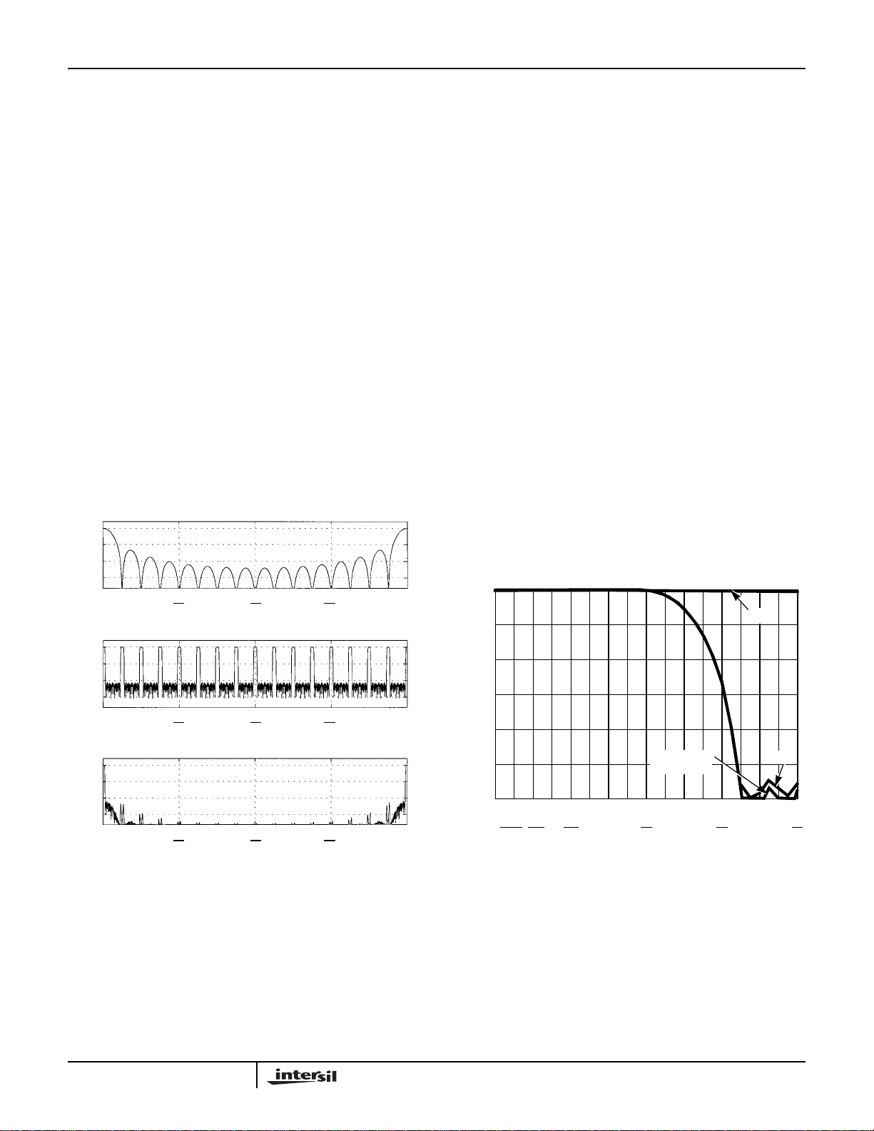
response of the HDF. The frequency responses of the HDF,
FIR, and Composite HDF/FIR filters are shown in Figure 8.
The composite passband of the HDF and FIR filter
frequency response is shown in Figure 9. The FIR
coefficients are scaled so that the maximum gain of the
composite filter is less than or equal to 0dB. The composite
passband ripple is less than 0.04dB.
)
)
)
HDF
0
-50
-100
-150
MAGNITUDE (dB)
(R = 16)
f
S
4
f
S
2
3f
S
4
FIR
0
-50
-100
-150
MAGNITUDE (dB)
f
S
4
f
S
2
3f
S
4
COMPOSITE
0
-50
-100
-150
MAGNITUDE (dB)
f
S
4
f
S
2
SAMPLE TIMES
3f
S
4
FIGURE 8A. DDC HDF, FIR, AND COMPOSITE FILTER
RESPONSE (FOR R = 16)
f
S
f
S
f
S
0
-20
-40
-60
-80
MAGNITUDE (dB)
-100
-120
2 4 6 8 10 12 14 16 18 20 22 24 26 28 30 32
f
S
128R
f
64R
f
S
S
32R
SAMPLE TIMES
COMPOSITE
f
S
16R
HDF/FIR
3f
32R
HDF
FIR
f
S
S
8R
FIGURE 8B. DDC FILTER RESPONSES (FOR R = 16)
3-207
 Loading...