

Intersil Corporation HSP48908-883 Datasheet
HSP48908/883
Data Sheet May 1999
Two Dimensional Convolver
The Intersil HSP48908/883 is a high speed TwoDimensional
Convolver which provides a single chip implementation of a
video data rate 3 x 3 kernel convolution on two dimensional
data. It eliminates the need for external data storage through
the use of the on-chip row buffers which are programmable
for row lengths up to 1024 pixels.
There are internal register banks for storing two independent
3 x 3 filter kernels, thus, facilitating the implementation of
adaptive filters and multiple filter operations on the same
data. The pixel data path also includes an on-chip ALU for
performing real-time arithmetic and logical pixel point
operations.
Data is provided to the HSP48908/883 in a raster scan
noninterlaced fashion, and is internally buffered on images
up to 1024 pixels wide for the 3 x 3 convolution operation.
Images with larger rows and convolution with larger kernel
sizes can be accommodated by using external row buffers
and/or multiple HSP48908/883s. Coefficient and pixel input
data are 8-bit signed or unsigned integers, and the 20-bit
convolver output guarantees no overflow for kernel sizes up
to 4 x 4. Larger kernel sizes can be implemented however,
since the filter coefficients will normally be less than their
maximum 8-bit values.
The HSP48908/883 is manufactured using an advanced
CMOS process, and is a low power fully static design. The
configuration of the device is controlled through a standard
microprocessor interface and all inputs/outputs are TTL
compatible.
File Number
2783.4
Features
• This Circuit is Processed in Accordance to MIL-STD-883
and is Fully Conformant Under the Provisions of
Paragraph 1.2.1.
• Single Chip 3 x 3 Kernel Convolution
• Programmable On-Chip Row Buffers
• DC to 27MHz Clock Rate
• Cascadable for Larger Kernels and Images
• On-Chip 8-Bit ALU
• Dual Coefficient Mask Registers, Switchable in a Single
Clock Cycle
• 8-Bit Signed or Unsigned Input and Coefficient Data
• 20-Bit Extended Precision Output
• Standard µP Interface
Applications
• Image Filtering
• Edge Detection
• Adaptive Filtering
• Real Time Video Filter
Ordering Information
TEMP.
PART NUMBER
HSP48908GM-20/883 -55 to 125 84 Ld PGA CMGA3-84
HSP48908GM-27/883 -55 to 125 84 Ld PGA CMGA3-84
RANGE (oC) PACKAGE PKG. NO.
1
CAUTION: These devices are sensitive to electrostatic discharge; follow proper IC Handling Procedures.
http://www.intersil.com or 407-727-9207
| Copyright © Intersil Corporation 1999
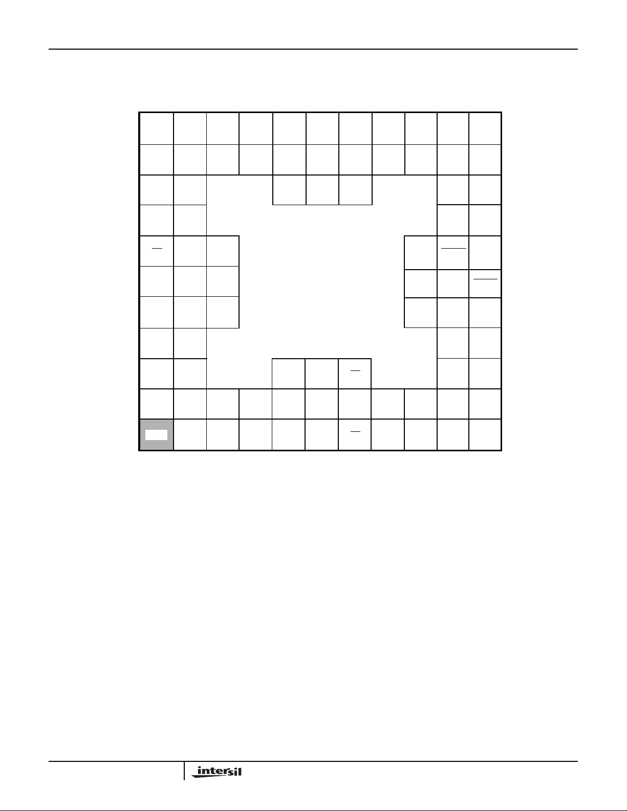
Pinouts
HSP48908/883
84 PIN PGA
TOP VIEW
CASO6 DOUT0 DOUT1 GND DOUT5 DOUT6 DOUT8 DOUT10 DOUT12 DOUT13 DOUT15
11
10
9
CASO1 CASO2
8
GND
OE
7
6
5
4
3
2
1
CASO0
DIN2 DIN3 DIN4
DIN5 DIN6
DIN7 CIN1
CIN0 CIN3 CIN4 GNDCIN7
CIN2
DOUT7DOUT3GNDCASO3
V
CC
DIN0DIN1 V
CIN9
HOLD
CLKCIN8CIN6CIN5
A1 A0 CASI15
CC
V
CC
FRAME
CASI2
CASI5 CASI4 CASI3
LD
A2 EALU CASI13V
CS
CASI10 CASI8
CASI11
CASI14 CASI12
DOUT17GNDDOUT14DOUT11GNDDOUT4DOUT2 DOUT9CASO5 CASO7CASO4
DOUT18DOUT16
GNDDOUT19
CASI0CASI1
RESET
CC
CASI7 CASI6
CASI9
ABCDEFGHJ KL
2
HSP48908/883
Absolute Maximum Ratings Thermal Information
Supply Voltage. . . . . . . . . . . . . . . . . . . . . . . . . . . . . . . . . . . . . +8.0V
Input, Output or I/O Voltage Applied . . . . .GND -0.5V to VCC +0.5V
ESD Classification . . . . . . . . . . . . . . . . . . . . . . . . . . . . . . . . .Class 1
Operating Conditions
Temperature Range. . . . . . . . . . . . . . . . . . . . . . . . . -55oC to 125oC
Voltage Range. . . . . . . . . . . . . . . . . . . . . . . . . . . . . +4.5V to +5.5V
CAUTION: Stresses above those listed in “Absolute Maximum Ratings” may cause permanent damage to the device. This is a stress only rating and operationofthe
device at these or any other conditions above those indicated in the operational sections of this specification is not implied.
NOTE:
1. θJA is measured with the component mounted on an evaluation PC board in free air.
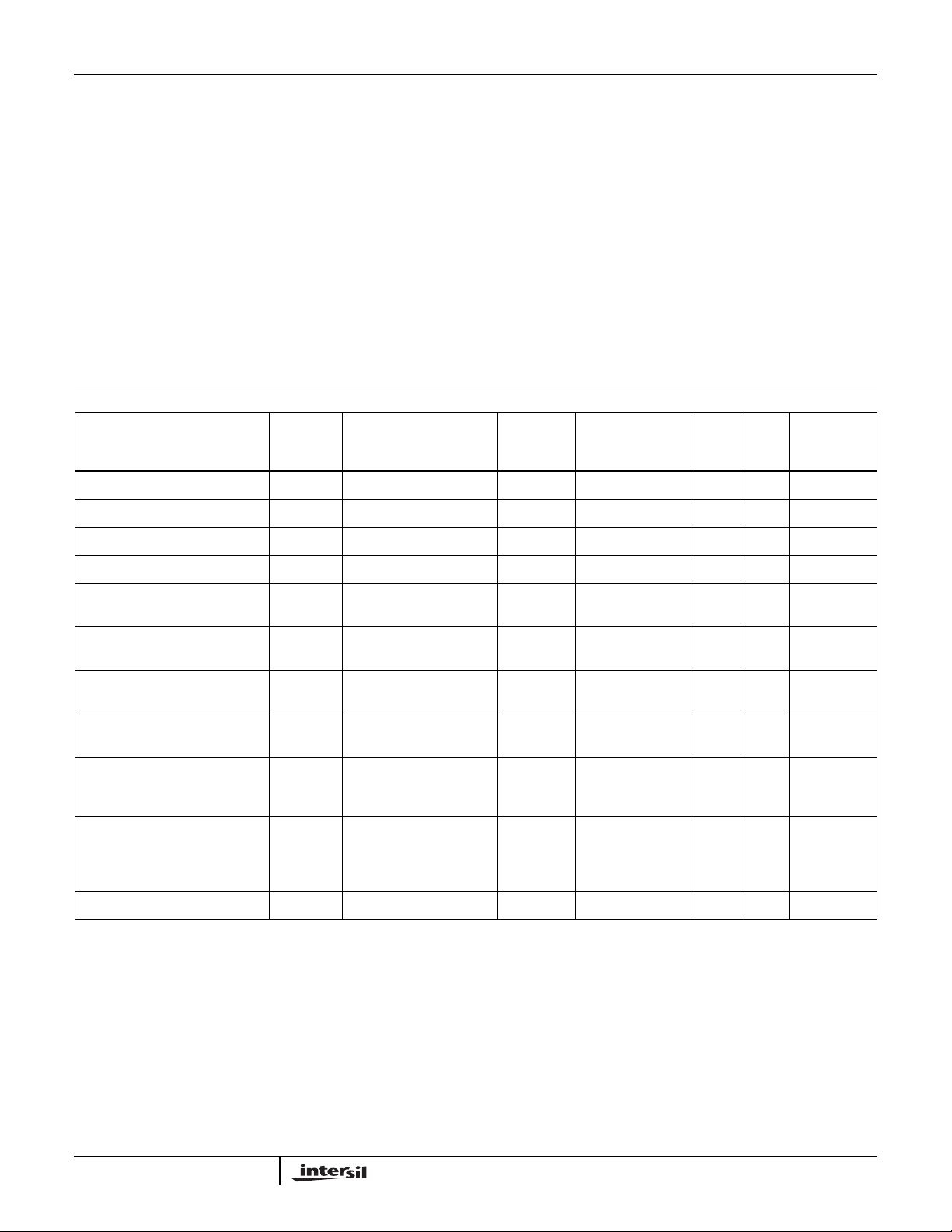
TABLE 1. DC ELECTRICAL PERFORMANCE SPECIFICATIONS
PARAMETER SYMBOL TEST CONDITIONS
Thermal Resistance (Typical, Note 1) θJA (oC/W) θJC (oC/W)
PGA Package. . . . . . . . . . . . . . . . . . 35.0 6.0
Maximum Package Power Dissipation at 125oC
PGA Package. . . . . . . . . . . . . . . . . . . . . . . . . . . . . . . . . . . .1.45W
Maximum Storage Temperature Range. . . . . . . . . . -65oC to 150oC
Maximum Junction Temperature . . . . . . . . . . . . . . . . . . . . . . .175oC
Maximum Lead Temperature (Soldering 10s) . . . . . . . . . . . . .300oC
Die Characteristics
Number of Transistors or Gates. . . . . . . . . . . . . 190,000 Transistors
GROUP A
SUB-
GROUP
TEMPERATURE
(oC) MIN MAX UNITS
Logical One Input Voltage V
Logical Zero Input Voltage V
Clock Input High V
Clock Input Low V
Output HIGH Voltage V
VCC = 5.5V 1, 2, 3 -55 ≤ TA≤ 125 2.2 - V
IH
VCC = 4.5V 1, 2, 3 -55 ≤ TA≤ 125 - 0.8 V
IL
VCC = 5.5V 1, 2, 3 -55 ≤ TA≤ 125 3.0 - V
IHC
VCC = 4.5V 1, 2, 3 -55 ≤ TA≤ 125 - 0.8 V
ILC
OH
IOH = 400mA,
1, 2, 3 -55 ≤ TA≤ 125 2.6 - V
VCC = 4.75V (Note 2)
Output LOW Voltage V
OL
IOL = +2.0mA,
1, 2, 3 -55 ≤ TA≤ 125 - 0.4 V
VCC = 4.5V (Note 2)
Input Leakage Current I
VIN = VCC or GND,
I
1, 2, 3 -55 ≤ TA≤ 125 -10 +10 µA
VCC = 5.5V
Output or I/O
Leakage Current
Standby Power Supply Current I
I
O
CCSB
V
= VCC or GND
OUT
VCC = 5.5V
VIN = VCC or GND,
1, 2, 3 -55 ≤ TA≤ 125 -10 +10 µA
1, 2, 3 -55 ≤ TA≤ 125 - 500 µA
VCC = 5.5V,
Outputs Open (Note 5)
Operating Power Supply Current I
CCOP
f = 20.0MHz,
1, 2, 3 -55 ≤ TA≤ 125 - 160.0 mA
VCC = 5.5V
Outputs Open,
(Note 3, 5)
Functional Test FT (Notes 4, 5) 7, 8 -55 ≤ TA≤ 125 - - -
NOTES:
2. Interchanging of force and sense conditions is permitted.
3. Operating supply current is proportional to frequency, typical rating is 8.0mA/MHz.
4. Tested as follows: f = 1MHz, VIH = 2.6, VIL = 0.4, VOH≥ 1.5V, VOL≤ 1.5V, V
= 3.4V, and V
IHC
ILC
= 0.4V.
5. Loading is as specified in the test load circuit with CL = 40pF.
3
 Loading...