

Intersil Corporation HSP48908 Datasheet

HSP48908
Data Sheet May 1999
Two Dimensional Convolver
The Intersil HSP48908 is a high speed Two Dimensional
Convolver which provides a single chip implementation of a
video data rate 3 x 3 kernel convolution on two dimensional
data. It eliminates the need for externaldatastoragethrough
the use of the on-chip row buffers which are programmable
for row lengths up to 1024 pixels.
There are Internal Register banks for storing two
independent 3 x 3 filter kernels, thus facilitating the
implementation of adaptive filters and multiple filter
operations on the same data. The pixel data path also
includes an on-chip ALU for performing real-time arithmetic
and logical pixel point operations.
Data is provided to the HSP48908 in a raster scan
noninterlaced fashion, and is internally buffered on images
up to 1024 pixels wide for the 3 x 3 convolution operation.
Images with larger rows and convolution with larger kernel
sizes can be accommodated by using external row buffers
and/or multiple HSP48908s. Coefficient and pixel input data
are 8-bit signed or unsigned integers, and the 20-bit
convolver output guarantees no overflow for kernel sizes up
to 4 x 4. Larger kernel sizes can be implemented however,
since the filter coefficients will normally be less than their
maximum 8-bit values.
The HSP48908 is manufactured using an advanced CMOS
process, and is a low power fully static design. The
configuration of the device is controlled through a standard
microprocessor interface and all inputs/outputs are TTL
compatible.
File Number
2456.5
Features
• Single Chip 3 x 3 Kernel Convolution
• Programmable On-Chip Row Buffers
• DC to 32MHz Clock Rate
• Cascadable for Larger Kernels and Images
• On-Chip 8-Bit ALU
• Dual Coefficient Mask Registers, Switchable in a
Single Clock Cycle
• 8-Bit Signed or Unsigned Input and Coefficient Data
• 20-Bit Extended Precision Output
• Standard µP Interface
• Low Power CMOS
Applications
• Image Filtering
• Edge Detection
• Adaptive Filtering
• Real Time Video Filter
Ordering Information
TEMP.
PART NUMBER
HSP48908VC-20 0 to 70 100 Ld MQFP Q100x14x20
HSP48908VC-32 0 to 70 100 Ld MQFP Q100x14x20
HSP48908JC-20 0 to 70 84 Ld PLCC N84.1.15
HSP48908JC-32 0 to 70 84 Ld PLCC N84.1.15
HSP48908GC-20 0 to 70 84 Ld PGA G84.A
HSP48908GC-32 0 to 0 84 Ld PGA G84.A
RANGE (oC) PACKAGE PKG. NO.
1
CAUTION: These devices are sensitive to electrostatic discharge; follow proper IC Handling Procedures.
http://www.intersil.com or 407-727-9207 | Copyright © Intersil Corporation 1999

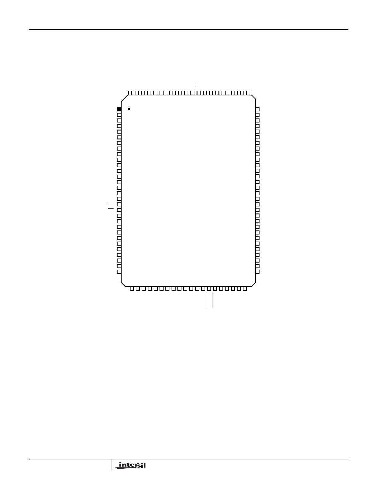
Pinouts
HSP48908
84 PIN PGA
TOP VIEW
DOUT8
DOUT10
DOUT12
DOUT14
DOUT13
GND
11
CAS06 DOUT15
DOUT0
DOUT1
10
CAS04
CAS06
CAS07
GND
DOUT2
DOUT5
DOUT4
DOUT6
DOUT9
GND
DOUT11
DOUT17
CASI1
CASI2
CASI6
CASI13
CASI16
DOUT16
DOUT19
FRAME
V
CC
CASI14
CASI7
CASI10
CASI11
CASI14
DOUT18
GND
CASI0
RESET
CASI13
CASI16
CASI18
CASI9
CASI12
9
CAS03
8
CAS01
7
6
5
4
3
2
1
OE
DIN1
DIN2
DIN5
DIN7
CIN0
CIN2
GND
CAS02
GND
CASO0
DIN3
DIN6
CIN1
CIN3
CIN5
BCDEFGHJKLA
V
CC
DIN0
DIN4
CIN4
CIN6
DOUT3 DOUT7 V
CIN9 HOLD L0
CIN7
GND
CIN8
CLK
CC
A2
CS
EALU
A0
V
CC
A1
2

HSP48908
Pinouts
(Continued)
CIN3
CIN4
CIN5
CIN6
CIN7
CIN8
CIN9
GND
CLK
V
CC
HOLD
LD
CS
A2
A1
A0
EALU
CASI15
CASI14
CASI13
CASI12
84 LEAD PLCC
TOP VIEW
CIN2
CIN1
CIN0
DIN7
DIN6
DIN5
DIN4
DIN3
DIN2
11 10 9 8 7 6 5 4 3 2 1 84 83 82 81 80 79 78 77 7675
12
13
14
15
16
17
18
19
20
21
22
23
24
25
26
27
28
29
30
31
32
33 34 35 36 37 3839 40 41 42 43 44 4546 47 48 49 50 51 5253
DIN1
DIN0
CC
V
OE
GND
CASO0
CASO1
CASO2
CASO3
CASO4
GND
CASO5
74
73
72
71
70
69
68
67
66
65
64
63
62
61
60
59
58
57
56
55
54
CASO6
CASO7
DOUT0
DOUT1
DOUT2
GND
DOUT3
DOUT4
DOUT5
DOUT6
DOUT7
V
CC
DOUT8
GND
DOU9
DOUT10
DOUT11
DOUT12
DOUT13
DOUT14
GND
CASI11
CASI10
CASI9
CASI8
CASI7
CASI6
CASI5
CASI4
CC
V
CASI3
CASI2
CASI1
CASI0
FRAME
GND
RESET
DOUT19
DOUT18
DOUT17
DOUT15
DOUT16
3
HSP48908
Pinouts
(Continued)
CIN1
CIN2
NC
NC
CIN3
CIN4
CIN5
CIN6
CIN7
CIN8
CIN9
GND
GND
CLK
V
CC
V
CC
HOLD
LD
CS
A2
A1
A0
EALU
CASI15
CASI14
CASI13
CASI12
NC
NC
CASI11
100 LEAD MQFP
TOP VIEW
CC
DIN0
DIN1
DIN2
DIN3
DIN4
DIN5
DIN6
DIN7
CIN0
99 98 97 96 95 94 93 91 89 87 85 84 83 818286889092100
1
2
3
4
5
6
7
8
9
10
11
12
13
14
15
16
17
18
19
20
21
22
23
24
25
26
27
28
29
30
VCCV
OE
GND
GND
CASO1
CASO0
CASO2
CASO3
CASO4
GND
80
79
78
77
76
75
74
73
72
71
70
69
68
67
66
65
64
63
62
61
60
59
58
57
56
55
54
53
52
51
GND
CASO5
NC
CASO6
CASO7
DOUT0
DOUT1
DOUT2
GND
GND
DOUT3
DOUT4
DOUT5
DOUT6
DOUT7
V
CC
V
CC
DOUT8
GND
GND
DOUT9
DOUT10
DOUT11
DOUT12
DOUT13
DOUT14
GND
GND
DOUT15
DOUT16
32 33 34 35 36 37 38 40 42 44 46 47 48 50494543413931
CASI9
CASI10
CASI8
CASI7
CASI5
CASI6
CASI3
CASI4
CC
CC
V
V
CASI2
CASI1
CASI0
RESET
FRAME
GND
GND
DOUT19
DOUT17
DOUT18
4

Block Diagram
HSP48908
DIN0 - 7
CIN0 - 9
FRAME
RESET
OE
DATA DELAY
-1
Z
Z-1Z-1Z-1Z
REGISTER
CONTROL
LOGIC
Z
ALU
ALU
-1
r
BUFFER
-1
CASCADE
-1
Z
-1
Z
-1
Z
CASIO - 7 CASIO - 15
ROW
2:1
MODE
Z
Z
Z
-1
-1
-1
r
ROW
BUFFER
CASCADE
MODE
2:1
2:1
Z
Z
Z
CASIO0 - 7
-1
-1
-1
HGIDEFABC
-1
Z
-1
Z
+ +
-1
-1
-1
Z
Z
Z
-1
Z
-1
-1
Z
Z
-1
Z
+
CASIO - 15
A0 - 2
LD
CS
CLK
HOLD
CASCADE
MODE
-1
Z
SHIFT
16
20
20
2:1
-1
Z
-1
Z
-1
Z
+
-1
Z
0
-1
Z
3
DOUTO - 19
ADDRESS
DECODER
CLOCK
GEN
INTERNAL CLOCK
5

HSP48908
Pin Descriptions
NAME PLCC PIN TYPE DESCRIPTION
V
CC
GND 19, 48, 54, 61,
CLK 20 I Input and System Clock. Operations are synchronous with the rising edge of this clock signal.
DIN-07 1-8 I Pixel Data Input Bus. This bus is used to provide the 8-bit pixel input data to the HSP48908. The
ClN0-9 9-18 I Coefficient Input Bus. This input bus is used to load the Coefficient Mask Register(s), the Initializa-
DOUT0-19 49-53, 55-60,
CASIO-15 29-41, 43-45 I Cascade Input Bus. This bus is used for cascading multiple HSP48908s to allow convolution with
CASO0-7 73-75, 77-81 0 Cascade Output Bus. This bus is used primarily during cascading to handle larger frames and/or
FRAME 46 I Frame is an asynchronous new frame or vertical sync input. A low on this input resets all internal
EALU 28 I Enable ALU Input.Thiscontrol line gates the clockto the ALU Register.When it is high, thedataon
HOLD 22 I The Hold Inputisused to gatethe clock fromall of theinternal circuitryofthe H5P48908. Thissignal
RESET 47 I Reset is an asynchronous signalwhichresets all internal circuitry of the HSP48908. All outputs are
OE 83 I Output Enable. The OEinputcontrols the state of the Output Databus (DOUT0-19). ALOW on this
A0-2 25-27 I Control Register Address. These lines are decoded to determine which register in the control logic
LD 23 I Load Strobe. LD is used for loading the Internal Registers of the HSP48908. When CS and LD are
CS 24 I Chip Select. The Chip Select input enables loading of the Internal Registers. When CS is low, the
21, 42, 63, 84 The +5V power supply pins. 0.1µF capacitors between the VCC and GND pins are
recommended.
The device ground.
69, 76, 82
data mustbe providedina synchronous fashion,and islatchedon the risingedge of theCLKsignal.
tion Register, the Row Buffer Length Register and the ALU microcode. It may also be used to provide a second operand input to the ALU. The definition of the ClN0-9 bits is defined by the register
address bits A0-2. The CIN0-9 data is loaded totheAddressedRegisterthrough the use of the CS
and LD inputs.
0 Output Data Bus. This 20-Bit output port is used to provide the convolution result. The result is the
62, 64-68,
70-72
sum ofproducts of theinputdata samples andtheir corresponding coefficients.The Cascade inputs
CASl0-15 may also be added totheresultby selecting the appropriate cascade mode in the Initialization Register.
larger kernels or row sizes. It may also be used to interface to external row buffers.Thefunction of
this bus is determined by theCascadeModebit (Bit 0) of the Initialization Register. When this bit is
set to a ‘0’, the value on CASI0-15 is left shifted and added to DOUT0-19. The amount of the shift
is determined by bits 7-8 oftheInitializationRegister. While this mode is intended primarily forcascading, it may also be used to add an offset value, such as to increase the brightness of the convolved image.
When the Cascade mode bit is set to a “1”, this bus is used for interfacing to external row buffers.
In this modethebus is divided into two8-bit busses (CASl0-7 and CASl8-15),thusallowing two additional pixel data inputs. The cascade data is sent directly to the internal multiplier array which allows for larger row sizes without using multiple HSP48908s.
kernel sizes. This output data is the data on DIN0-7 delayed bytwicetheprogrammed internal row
buffer length.
circuitry except for the Coefficient, ALU, AMC, EOR and INT Registers. Thus, after a Frame reset
has occurred, a new frame of pixels may be convolved without reloading these registers.
CIN0-7 is loaded onthenext rising clockedge. When EALU islow,thelastvalue loaded remains in
the ALU Register.
is synchronous, is sampledonthe rising edge of CLK and takes effectonthefollowing cycle. While
this signal is active (high), the clock will have no effect on the HSP48908 and
internal data will remain undisturbed.
forced low in the reset state.
control line enablestheport foroutput. When OE is HIGH, the output drivers areinthe high impedance state. Processing is not interrupted by this pin.
is the destination for the data on the ClN0-9 inputs. Register loading is controlled by the A0-2, LD
and CS inputs.
active, the rising edge of LD will latch the CIN0-7 data into the register specified by A0-2.
A0-2 addresslinesare decoded todeterminethe meaning of thedata on the CIN0-7bus. The rising
edge of LD will then load the Addressed Register.
6
 Loading...