Intersil Corporation HSP48901 Datasheet

HSP48901
Data Sheet May 1999
3 x 3 Image Filter
The Intersil HSP48901 is a high speed 9-Tap FIR Filter
which utilizes 8-bit wide data and coefficients. It can be
configured as a one dimensional (1-D) 9-Tap filter for a
variety of signal processing applications, or as a two
dimensional (2-D) filter for image processing. In the 2-D
configuration, the device is ideally suited for implementing 3
x 3 kernel convolution. The 30MHz clock rate allows a large
number of image sizes to be processed within the required
frame time for real-time video.
Data is provided to the HSP48901 through the use of
programmable data buffers such as the HSP9500 or any
other Programmable Shift Register. Coefficient and pixel
input data are 8-bit signed or unsigned integers, and the
20-bit extended output guarantees no overflow will occur
during the filtering operation.
There are two internal register banks for storing independent
3 x 3 filter kernels, thus, facilitating the implementation of
adaptive filters and multiple filter operations on the same
data.
The configuration of the HSP48901 Image Filter is controlled
through a standard microprocessor interface and all inputs
and outputs are TTL compatible.
File Number
2459.5
Features
• DC to 30MHz Clock Rate
• Configurable for 1-D and 2-D Correlation/Convolution
• Dual Coefficient Mask Registers, Switchable in a Single
Clock Cycle
• Two’s Complement or Unsigned 8-Bit Input Data and
Coefficients
• 20-Bit Extended Precision Output
• Standard µP Interface
Applications
• Image Filtering
• Edge Detection/Enhancement
• Pattern Matching
• Real Time Video Filters
Ordering Information
TEMP.
PART NUMBER
RANGE (oC) PACKAGE
HSP48901JC-20 0 to 70 68 Ld PLCC N68.95
HSP48901JC-30 0 to 70 68 Ld PLCC N68.95
HSP48901GC-20 0 to 70 68 Ld PGA G68.A
HSP48901GC-30 0 to 70 68 Ld PGA G68.A
PKG.
NO.
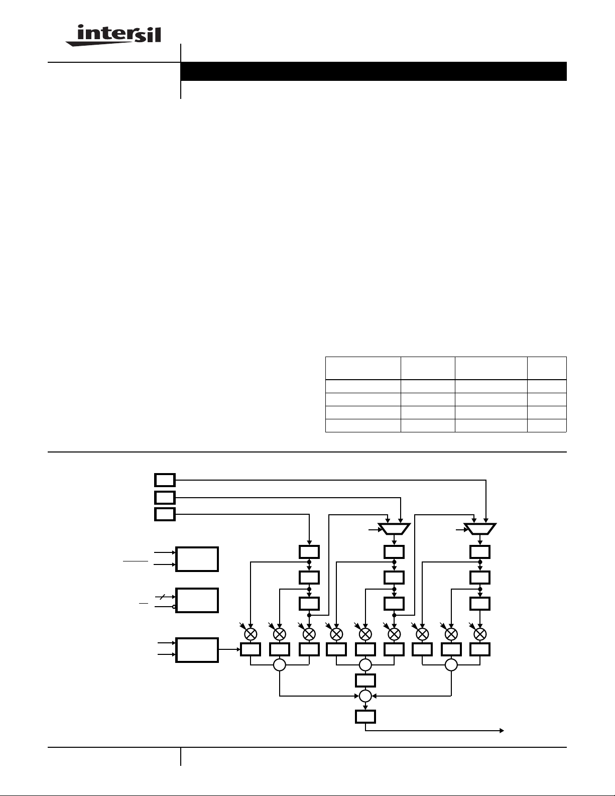
Block Diagram
DIN3 (0-7)
DIN2 (0-7)
DIN1 (0-7)
FRAME
CIN0-7
A0-2
LD
CLK
HOLD
-1
Z
-1
Z
-1
Z
3
CONTROL
LOGIC
ADDRESS
DECODER
INTERNAL
CLOCK
CLOCK
GEN
MODE MODE
-1
Z
-1
Z
-1
Z
-1
-1
-1
Z
Z
Z
+ + +
-1
Z
2:1
-1
Z
-1
Z
-1
Z
-1
-1
-1
Z
-1
Z
+
-1
Z
Z
Z
2:1
-1
Z
-1
Z
-1
Z
ABCDEFGHI
-1
-1
Z
Z
DOUT 0-19
1
CAUTION: These devices are sensitive to electrostatic discharge; follow proper IC Handling Procedures.
http://www.intersil.com or 407-727-9207 | Copyright © Intersil Corporation 1999

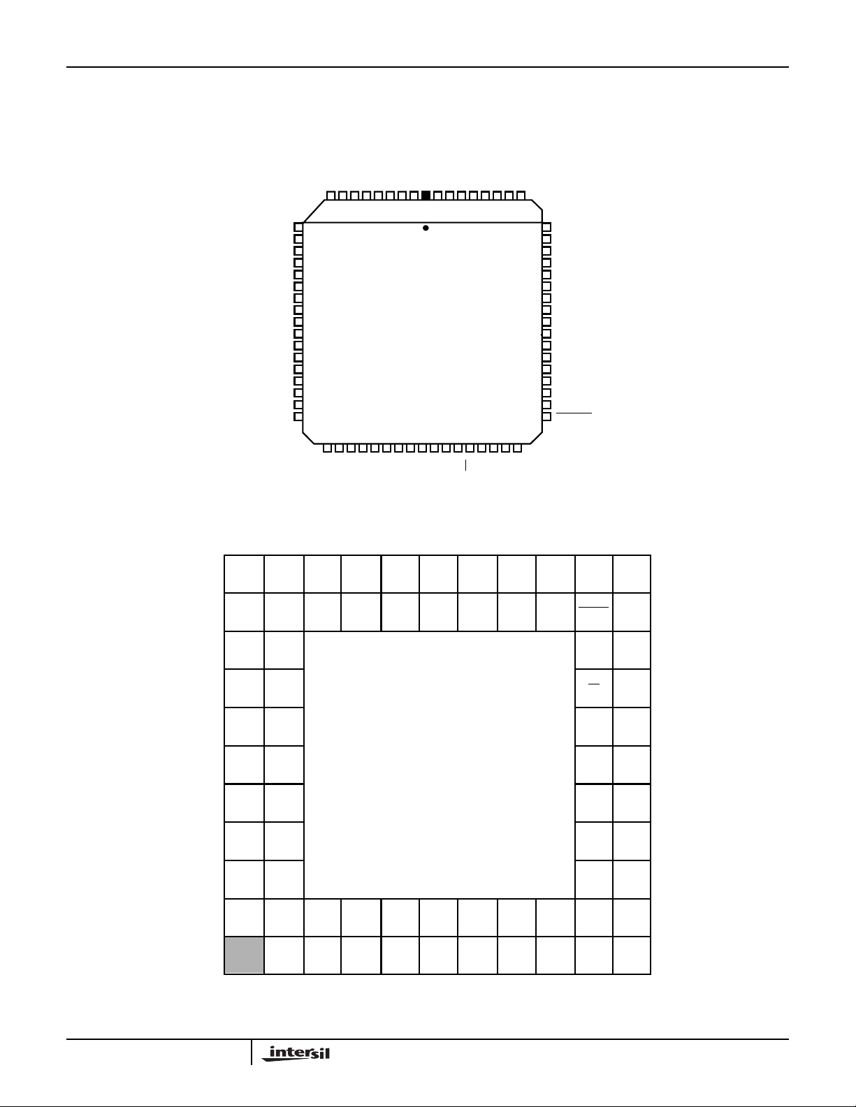
Pinouts
HSP48901
68 LEAD PLCC
TOP VIEW
DOUT3
A2A1A0
HOLD
DOUT4
DOUT5
4327 28 29 30 31 32 33 34 35 36 37 38 39 40 41 42
CC
V
DOUT6
60
DOUT7
59
DOUT8
58
DOUT9
57
GND
56
DOUT10
55
DOUT11
54
DOUT12
53
DOUT13
52
DOUT14
51
DOUT15
50
DOUT16
49
DOUT17
48
DOUT18
47
DOUT19
46
V
45
CC
FRAMES
44
DIN2 (7)
DIN2 (6)
DIN2 (5)
DIN2 (4)
DIN2 (3)
DIN2 (2)
DIN2 (1)
DIN2 (0)
GND
DIN3 (7)
DIN3 (6)
DIN3 (5)
DIN3 (4)
DIN3 (3)
DIN3 2)
DIN3 (1)
DIN3 (0)
VCCDIN1 (0)
DIN1 (1)
DIN1 (2)
DIN1 (3)
DIN1 (4)
DIN1 (5)
DIN1 (6)
DIN1 (7)
GND
DOUT0
DOUT1
DOUT2
9 8 7 6 5 4 3 2 1 6867666564636261
10
11
12
13
14
15
16
17
18
19
20
21
22
23
24
25
26
CC
V
CLK
GND
CIN7
CIN6
CIN5
CIN4
CIN3
CIN2
CIN1
CIN0
GND
LD
68 PIN GRID ARRAY (PGA)
TOP VIEW
11
DOUT6
DOUT7
DOUT9
DOUT10
DOUT12
DOUT14
DOUT16
DOUT18
V
CC
10
DOUT5
9
DOUT3
8
DOUT1
7
GND
DIN1 (6)
6
5
DIN1 (4)
4
DIN1 (2)
3
DIN1 (0)
2
V
CC
1
V
CC
DOUT4
DOUT2
DOUT0
DIN1 (7)
DIN1 (5)
DIN1 (3)
DIN1 (1)
DIN2 (7)
DIN2 (6)
BCDEFGHJKLA
DOUT6
DIN2 (5)
DIN2 (4)
GND
DIN2 (3)
DIN2 (2)
DOUT11
DIN2 (1)
DIN2 (0)
DOUT13
GND
DIN2 (7)
DOUT15
DIN3 (6)
DIN3 (5)
DOUT17
DIN3 (4)
DIN3 (3)
DOUT19
DIN3 (2)
DIN3 (1)
FRAME
A2
LD
CIN0
CIN2
CIN4
CIN6
GND
V
CC
DIN3 (0)
A0
A1
HOLD
GND
CIN1
CIN3
CIN5
CIN7
CLK
2

HSP48901
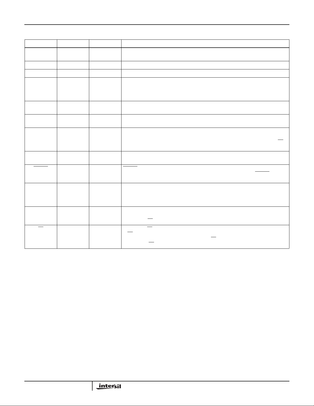
Pin Descriptions
NAME PLCC PIN TYPE DESCRIPTION
V
CC
GND 18, 29, 38, 56 The device ground.
CLK 28 I Input and System clock. Operations are synchronous with therising edgeof this clock signal.
DIN1(7-0) 1-8 I Pixel Data Input Bus #1. These inputs are used to provide 8-bit pixel data to the HSP48901.
DIN2(7-0) 10-17 I Pixel Data Input Bus #2. Same as above. These inputs should be grounded when operating
DIN3(7-0) 19-26 I Pixel Data Input Bus #3. Same as above. These inputs should be grounded when operating
CIN7-0 30-37 I Coefficient Data Input Bus. This input bus is used to load the Coefficient Mask Register(s)
DOUT19-0 46-55, 57-60,
FRAME 44 I FRAME is an asynchronous new frame or vertical sync input. A low on this input resets all
HOLD 40 I The Hold Input is used to gate the clock from all of the internal circuitry of the HSP48901.
A2-0 41-43 I Control RegisterAddress. These linesare decodedto determine whichregister in thecontrol
LD 39 I Load Strobe. LD is usedfor loading the Internal Registers of theHSP48901. The rising edge
9, 27, 45, 61 The +5V power supply pins. 0.1µF capacitors between the VCC and GND pins are
recommended.
The data must be provided in a synchronous fashion, andis latched on the rising edge of the
CLK signal. The DIN1(0-7) inputs are also used to input data when operating in the 9-Tap
FIR mode.
in the 1D mode.
in the 1D mode.
and the Initialization Register. The register to be loaded is defined by the register address
bits A0-2. The CIN0-7 data is loaded to the addressed register through the use of the LD
input.
O Output Data Bus. This 20-Bit output port is used to provide the convolution result. The result
62-67
is the sum of products of the input data samples and their corresponding coefficients.
internalcircuitry except for the Coefficientand INT Registers. Thus, aftera FRAME resethas
occurred, a new frame of pixels may be convolved without reloading these registers.
This signal is synchronous, is sampled on the rising edge of CLK and takes effect on the
following cycle. While this signal is active (high), the clock will have no effect on the
HSP48901 and internal data will remain undisturbed.
logic is the destination for the data on the CIN0-7 inputs. Register loading is controlled by
the A0-2 and LD inputs.
of LD will latch the CIN0-7 data into the register specified by A0-2. The Address on A0-2
must be setup with respect to the falling edge of LD and must be held with respect to the
rising edge of LD.
3
 Loading...