HSP48212
Data Sheet May 1999
Digital Video Mixer
The Intersil HSP48212 is a 68 pin Digital Video Mixer IC
intended for use in multimedia and medical imaging
applications.
The HSP48212 allows the user to mix two video sources
based on a programmable weighting f actor. After weighting
the input data signals, the Video Mixer simply adds the two
weighted signals mathematically. This results in the mixed
output, which is a weighted sum of the two sources.
The input and output interfaces are synchronous with respect
to the input clock, simplifying the user interface requirements.
Input Data (DINA, DINB), Mix Factor (M) and control signals
(RND, TCB) may be delayed relative to each other in order to
compensate for any misalignment that may have occurred
prior to entering the HSP48212. Each input’s delay ma y be
independently programmed up to seven clock cycles.
The output data may be rounded to 8, 10, 12, or 13-bits. The
enabling of data onto the output data bus is under the user’s
control via an output enable signal (
OE).
Ordering Information
TEMP.
PART NUMBER
HSP48212VC-40 0 to 70 64 Ld MQFP Q64.14x14
HSP48212JC-40 0 to 70 68 Ld PLCC N68.95
RANGE (oC) PACKAGE PKG. NO.
File Number
3627.2
Features
• 12-Bit Pixel Data
• Two’s Complement or Unsigned Data
• 12-Bit Mix Factor
• 13-Bit Signed or Unsigned Three State Output
• Overflow Detection and Output Saturation
• Rounding to 8, 10, 12, or 13-Bits
• Input and Output Pixel Data Synchronous to Clock
• Programmable Pipeline Delay of up to 7 Clock Cycles for
Control of Misaligned Input Data
• TTL Compatible Inputs/Outputs
• DC to 40MHz Clock Rate
Applications
• Video Summing (Frame Addition)
• Video Mixing
• Fade In/Out
• Video Switching
• High Speed Multiplying
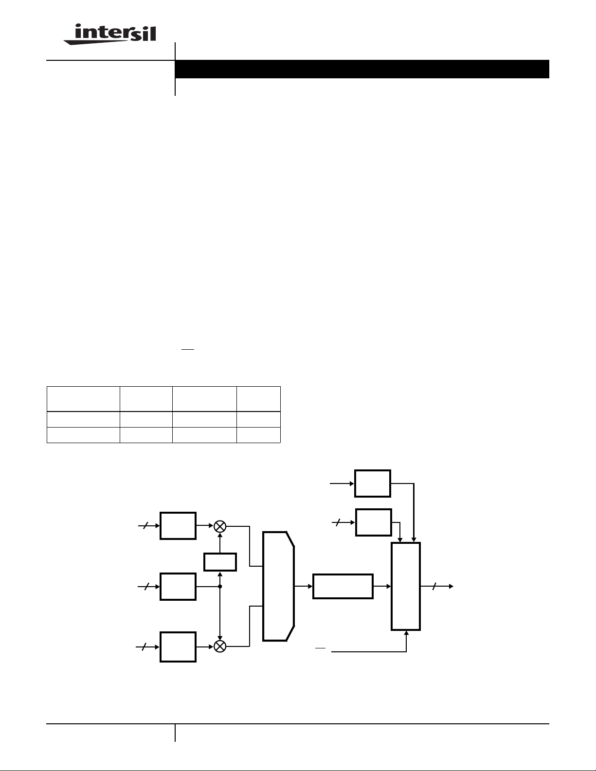
Block Diagram
DINB0-11
DINA0-11
DOUT = 2 x [DINA x M + DINB x (1-M)]
2
SHIFT
LEFT
DELAY
0-7
DELAY
0-7
OUTPUT
FORMAT
DOUT0-12
13
TCB
DELAY
DELAY
DELAY
1
0-7
1-M
0-7
0-7
CAUTION: These devices are sensitive to electrostatic discharge; follow proper IC Handling Procedures.
12
M
12
12
RND0-1
Σ
OE
http://www.intersil.com or 407-727-9207 | Copyright © Intersil Corporation 1999

Pinouts
DINB11
DINB10
DINB9
DINB8
DINB7
DINB6
GND
DINB5
DINB4
DINB3
DINB2
DINB1
DINB0
RND1
RND0
DELAY
HSP48212
64 LEAD MQFP
TOP VIEW
CC
CLK
MIXENM0M1M2M3M4M5M6M7
6463 62 61 60 59 58 57 56 55 54 53 52 51 50 49
1
2
3
4
5
6
7
8
9
10
11
12
13
14
15
16
17 1819 20 2122 23 24 25 26 27 28 29 30 31 32
V
M8M9M10
M11
48
47
46
45
44
43
42
41
40
39
38
37
36
35
34
33
BYPASS
OE
DOUT12
DOUT11
DOUT10
DOUT9
GND
DOUT8
DOUT7
DOUT6
DOUT5
V
CC
DOUT4
DOUT3
DOUT2
DOUT1
DOUT0
DINB11
DINB10
DINB9
DINB8
DINB7
DINB6
GND
DINB5
N/C
DINB4
DINB3
DINB2
DINB1
DINB0
RND1
RND0
DELAY
DINA10
DINA11
CC
V
DINA9
DINA8
DINA7
DINA6
DINA5
GND
DINA4
LD
TC
68 PIN PLCC
TOP VIEW
CC
CLK
MIXENM0M1M2M3M4M5
9876543216867666564636261
10
11
12
13
14
15
16
17
18
19
20
21
22
23
24
25
26
N/CM6M7
V
M8M9M10
DINA3
DINA2
DINA1
DINA0
M11
BYPASS
60
59
58
57
56
55
54
53
52
51
50
49
48
47
46
45
44
4327282930313233343536373839404142
OE
DOUT12
DOUT11
DOUT10
DOUT9
GND
DOUT8
DOUT7
N/C
DOUT6
DOUT5
V
CC
DOUT4
DOUT3
DOUT2
DOUT1
DOUT0
DINA10
DINA11
CC
V
DINA9
DINA8
DINA7
N/C
DINA6
DINA5
GND
DINA4
DINA3
DINA2
DINA1
DINA0
LD
TC
2

HSP48212
Pin Descriptions
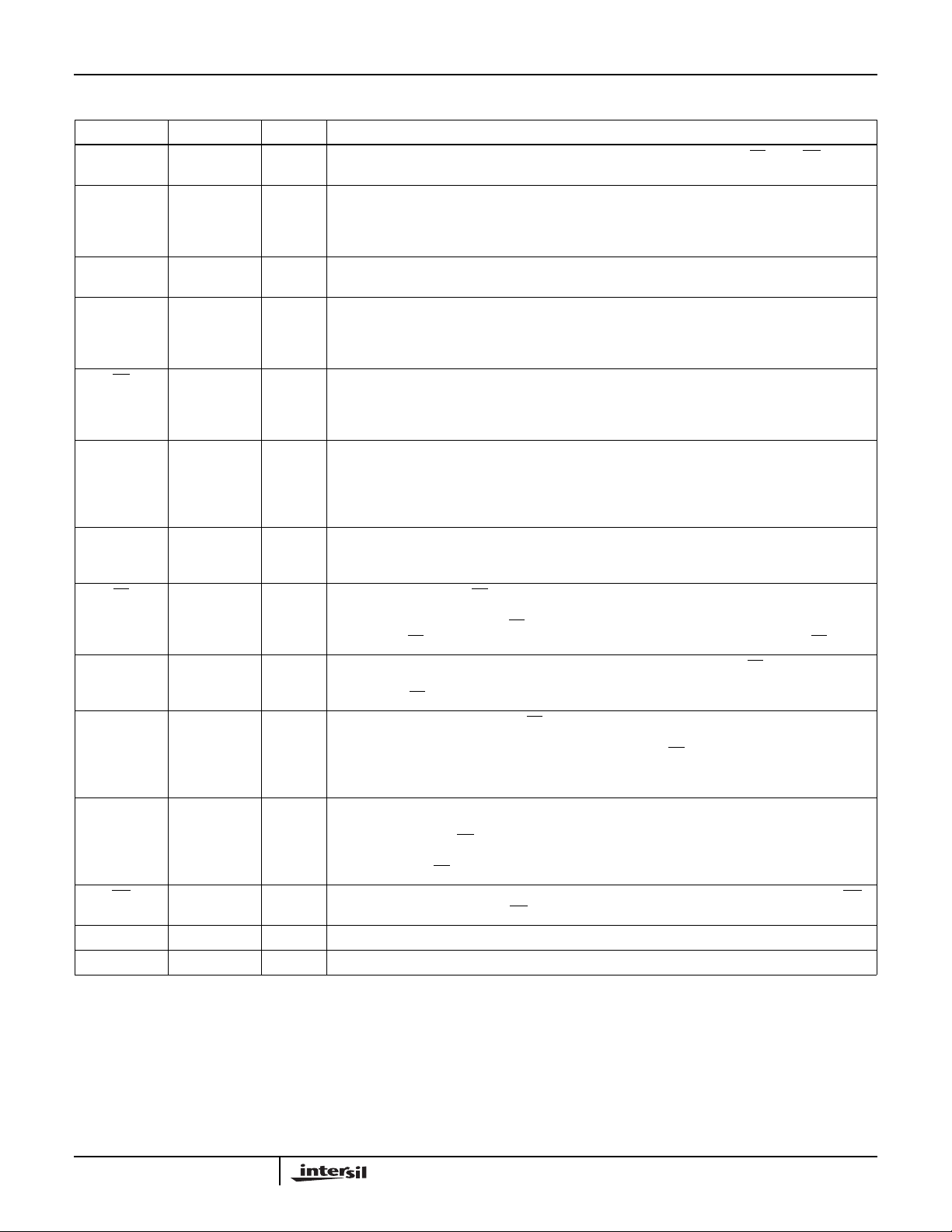
NAME PLCC PIN TYPE DESCRIPTION
CLK 9 I Clock Input. All signal pins are synchronous with respect to this clock except LD, DEL, OE, and BY-
PASS.
DINA0-11 29-31
33-34
36-38
40-43
DINB0-11 10-15, 17
19-23
M0-11 62-65
67-68
2-7
TC 28 I Specifies the number format of the input data busses DINA and DINB. 1 = unsigned, 0 = 2’s com-
RND0-1 24-25 I Specifies the number of significant bits on the output bus. 00 = 8-bit, 01 = 10-bit,
MIXEN 8 I Mix Enable. This pin is used to disable the clock signal which samples the Mix input. When MIXEN
LD 27 I Asynchronous Load Pin. LD is used to load the delay control registers. The delay control word is
DEL 26 I Delay Input. This is the serial input data that is sampled by the rising edge of LD. It is the input to the
BYPASS 61 I Allows user to disable (bypass) the LD interface and use the default delay paths. When BYPASS =
DOUT0-12 59-56
54-53
51-50
48-44
OE 60 I Output Enable. Asynchronous input which takes effect immediately following a transition. When OE =
V
CC
GND 16, 39, 55 I 0V power supply. There are 3 GND pads.
32, 49, 66 I 5V power supply. There are 3 VCC pads.
I Input Data Bus. Provides data to the Mixer from one video source. Synchronous to the rising edge
of CLK.
I Input Data Bus. Provides data to the Mixer from one video source. Synchronous to the rising edge
of CLK.
I Mix Input Bus. The range of M is from 0 to 1. The number format is unsigned, with one bit position
to the left of the binary point. If a value greater than 1 is placed on this bus,the internal circuitry will
saturate M to 1, i.e, anytime the MSB is 1, the internal value defaults to 1.00000000000; synchronous to the rising edge of CLK.
plement. The signal has the same number of latency stages as the incoming data. Therefore, the
number format affects the incoming data but not the data in the internal pipeline stages. Synchronous to the rising edge of CLK.
10 = 12-bit, 11 = 13-bit. Rounding is performed by adding a binary 1 to the bit position to the right of
the desired LSB.The remaining bits areforced to zero. These controlsignals have the same number
of latency stages as the incoming data. Therefore, the output round format does not take effect until
the current data has propagated to the output. Synchronous to the rising edge of CLK.
= 1, the M0-11 bus is sampledbythe rising edge of CLK. WhenMIXEN = 0,the M0-11 busis ignored
and the previously stored value of M0-11 is used. Synchronous to the rising edge of CLK.
loaded serially from LSB to MSB. This signal drives the clock input to a
15-bit serial shift register. Each LD cycle, the data is transferred through the register bank on the
rising edge of LD In order to load thedelay control word,the user must supply exactly15 LD pulses.
first stage ofthe 15-bit serial shift registerwhich contains the delay control word.Synchronous to the
rising edge of LD.
1, the delay control word is forced to all 0’sand no extra delaysare included in the paths. When BYPASS = 0, the delay control word must be initialized using the LD/DEL interface in order for the chip
to give predictable results. This pin is asynchronous and is not intended to change states during operation.
O Output Data Bus. The data on this bus reflects the results of the equation:
2x[AxM + Bx(1-M)]. The number format of the output is either 2’s complement or unsigned depending on the value of the TC signal during data input. The representation of DOUT is also dependent
on the value sampled on RND0-1 during data input.
(See RND0-1 and TC pin description).
0 the DOUT bus is driving, when OE = 1 the DOUT bus is not driven (floating).
3
 Loading...