

TM
HSP45314
Data Sheet May 2000
CommLinkTMDirect Digital Synthesizer
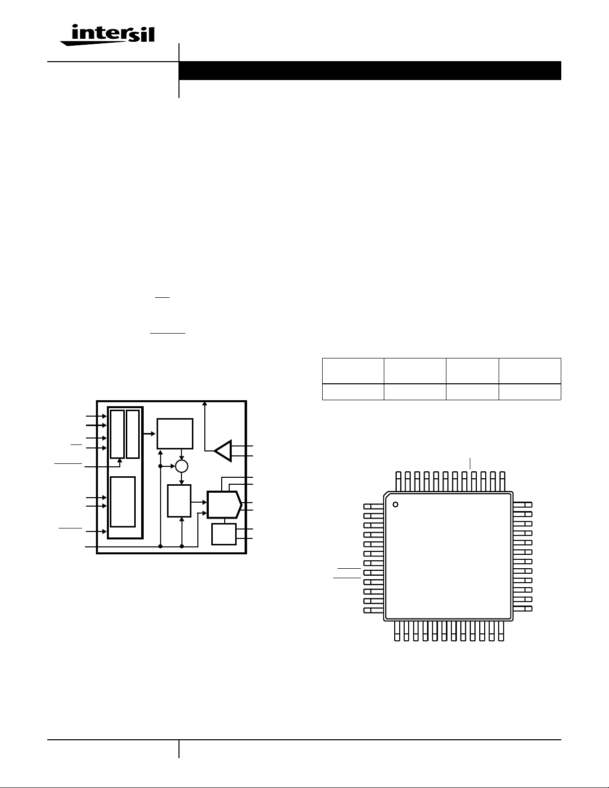
The 14-bit HSP45314 provides a complete Direct Digital
Synthesizer (DDS) system in a single 48-pin LQFP package.
A 48-bit Programmable Carrier NCO (numerically controlled
oscillator) and a high speed 14-bit DAC (digital to analog
converter) are integrated into a stand alone DDS.
The DDS accepts 48-bit center and offset frequency control
information via a parallel processor interface. Modulation
control is provided by 3 external pins.The PH0 and PH1 pins
select phase offsets of 0, 90, 180 and 270 degrees, while the
ENOFR pin enables or zeros the offset frequency word to
the phase accumulator.
The parallel processor interface has an 8-bit write-only data
input C(7:0), a 4-bit address A(3:0) bus, a Write Strobe
(WR), and a Write Enable (
WE). The processor can update
all registers simultaneously by loading a set of master
registers, then transfer all master registers to the slave
registers by asserting the
UPDATE pin.
Block Diagram
File Number 4820.2
Features
• 125MSPS Output Sample Rate with 5V Digital Supply
• 100MSPS Output Sample Rate with 3.3V Digital Supply
• 14-bit DAC with Internal Reference
• ParallelControlInterfacefor FastTuning(50MSPSControl
Register Write Rate)
• 48-bit Programmable Frequency Control
• Small 48-pin LQFP package
Applications
• Programmable Local Oscillator
• FSK Modulation
• Direct Digital Synthesis
• Clock Generation
Ordering Information
PART
NUMBER
HSP45314VI -40 to 85 48 LQFP Q48.7X7A
TEMP. RANGE
(oC) PACKAGE PKG. NO.
C(7:0)
A(3:0)
WR
WE
UPDATE
ENOFR
PH(1:0)
RESET
CLK
MASTER
SLAVE
MODULATION
CONTROL
PHASE
ACCUM.
∑
SINE
WAVE
ROM
COMPOUT
+
14 BIT
DAC
INT
REF
ININ+
COMP1
COMP2
IOUTA
IOUTB
REFIO
REFLO
Pinout
ENOFR
DGND
CLK
DVDD
RESET
UPDATE
COMPOUT
REFLO
REFIO
C2
C1
C0
48-PIN LQFP (Q48.7X7A
TOP VIEW
C7
C5
AGND
AGND
DVDD
C6
HSP45314
IOUTA
IOUTB
WR
COMP2
C3
1
2
3
4
5
6
7
8
9
10
11
12
13 14 1516
FSADJ
COMP1
C4
WE
DGND
AVDD
AGND
NC
IN+
A0
IN-
373839404142434445464748
2423222120191817
A1
36
35
34
33
32
31
30
29
28
27
26
25
AGND
A2
A3
PH0
PH1
DGND
DVDD
DGND
DGND
DGND
DGND
DVDD
DGND
3-1
1-888-INTERSIL or 321-724-7143 | Intersil and Design is a trademark of Intersil Corporation. | Copyright © Intersil Corporation 2000
CAUTION: These devices are sensitive to electrostatic discharge; follow proper IC Handling Procedures.
CommLink™ is a trademark of Intersil Corporation.

HSP45314
Typical Application Circuit (Sinewave Generation)
WRITE CLOCK
WRITE ENABLE
PH1:PH0 BUS
CLOCK
SOURCE
µPROCESSOR/
FPGA/CPLD
DV
PP
0.1µF
A3:A0 BUS
C7:C0 BUS
COMPOUT
0.1µF
C2
C1
C0
ENOFR
DGND
CLK
DVDD
RESET
UPDATE
REFLO
REFIO
R
SET
2kΩ
C3
1
2
3
4
5
6
7
8
9
10
11
12
13 14 15 16
FSADJ
0.1µF
AV
C4
COMP1
PP
C6
C5
HSP45314
AGND
AGND
IOUTB
C7
DVDD
IOUTA
0.1µF
WR
DGND
AVDD
COMP2
WE
AGND
NC
IN+
A0
IN-
373839404142434445464748
2423222120191817
A1
36
35
34
33
32
31
30
29
28
27
26
25
AGND
0.1µF
A2
A3
PH0
PH1
DGND
DVDD
DGND
DGND
DGND
DGND
DVDD
DGND
AV
PP
DV
0.1µF
DV
0.1µF
PP
PP
+5V POWER SOURCE
3-2
+
+
10µF
10µF
FERRITE
BEAD
10µH
FERRITE
BEAD
10µH
50Ω
50Ω
0.1µF
0.1µF
(IOUTA) ANALOG OUTPUT
DV
(DIGITAL POWER PLANE)
PP
1µF
AV
(ANALOG POWER PLANE)
PP
1µF

HSP45314
Functional Description
The HSP45314 is an NCO with an integrated 14-bit DAC
designed to run in excess of 125MSPS. The NCO is a 16-bit
output design, which is rounded to 14 bits for input to the
DAC. The frequency control is the sum of a 48-bit center
frequency word and a 48-bit offset frequency word. The two
components are added modulo 48 bits with the alignment
shown in Table 1. Each of the two terms can be zeroed
independently (via the microprocessor interface for the
center frequency and via the ENOFR pin for the offset
frequency term).
Frequency Generation
The output frequency of the part is determined by the
summation of two registers:
f
= f
OUT
where CF is the Center Frequency register and OF is the
Offset Frequency register.
With a 125MSPS clock rate, the center frequency can be
programmed to
(125 x 10
The addition of the frequency control words can be
interpreted as two’s complement if convenient. For example,
if the center frequency is set to 4000...00h and the offset
frequency set to C000..00h, the programmed center
frequency would be f
frequency -f
because only the lower 48 bits are retained, the effective
frequency would be 0. In reality, frequencies above
8000...00h alias below f
so the MSB is only provided as a convenience for two’s
complement calculations.
The frequency control of the NCO is the change in phase per
clock period or dφ/dt. This is integrated by the phase
accumulator to obtain frequency. The most significant 24
bits of phase are then mapped to 16 bits of amplitude in a
sine look-up table function. The range of dφ/dt is 0 to 1 with
1 equaling 360 degrees or (2 x pi) per clock period. The
phase accumulator output is also 0 to 1 with 1 equaling 360
degrees. The operations are modulo 48 bits because the
MSB (bit 47) aligns with the most significant address bit of
the sine ROM and the ROM contains one cycle of a sinusoid.
The MSB is weighted at 180 degrees. Full scale is 360
degrees minus 1 LSB and the phase then rolls over to 0
degrees for the next cycle of the sinusoid.
x ( (CF + OF) mod (248))/ (248),
CLK
6
)/(248) = 0.4 µHz resolution.
/4 and the programmed offset
CLK
/4. The sum would be 10000..00h, but
CLK
/2 (the output of the part is real),
CLK
Parallel Interface
The processor interface is an 8-bit parallel write only
interface. The interface consists of 8 data bits (C7:C0), four
address pins (A3:A0), a Write Strobe (WR), and a Write
Enable (
processor interface loads a set of master registers. The
contents of the master set of registers is then transferred to
a slave set of registers by asserting a pin (
allows all of the bits of the frequency control to be updated
simultaneously.
The rate which the user writes (WR) to these registers does
not have to be the same rate as the DDS clock rate (the rate
of the NCO and DAC; pin CLK). It is expected that most
applications will have a slower register write rate than the
DDS clock rate. It takes 6 WR cycles at the write rate plus
another 11 CLK cycles at the DDS rate to write and obtain a
new frequency, assuming that all registers are rewritten and
the
active until after the new word has been written, it takes 14
CLK cycles, rather than 11. For cases which require the
output to be updated with all of the new frequency
information present, it is necessary that the
inactive until after all of the new frequency word has been
written to the device. See the Timing Diagrams for more
information. The parallel registers can be written to again
immediately after the 11th or 14th CLK cycle, again
depending the state of
need 48 bits (all 6 registers) of frequency information, then
the output frequency can be changed more quickly. For
example, if only 32 bits of frequency information are needed
and it is desired that the output be updated all at once, then
it takes 4 WR cycles, then the assertion low of the
pin, plus another 14 CLK cycles at the DDS rate to write and
update a new frequency.
The timing is the same whether writing to the center or offset
frequency registers. For faster frequency update, consider
the ENOFR (Enable Offset Frequency Register) option.
Once the values have been written to the center and offset
frequency registers, the user can enable and disable the
offset frequency register, which is added to the center
frequency value when enabled. The ENOFR pin has a
latency of 14 CLK cycles, but simplifies the interface
because the only pin that has to be toggled is the ENOFR
pin.
WE). The interface is a master/slave type. The
UPDATE). This
UPDATE pin is always active. If the UPDATE pin is not
UPDATE be
UPDATE. If the application does not
UPDATE
TABLE 1. FREQUENCY CONTROL BIT ALIGNMENTS
Bits 4444 4444 3333 3333 3322 2222 2222 1111 1111 1100 0000 0000
Individual Bit Alignment 7654 3210 9876 5432 1098 7654 3210 9876 5432 1098 7654 3210
Phase Accumulator xxxx xxxx xxxx xxxx xxxx xxxx xxxx xxxx xxxx xxxx xxxx xxxx
Center Frequency xxxx xxxx xxxx xxxx xxxx xxxx xxxx xxxx xxxx xxxx xxxx xxxx
Offset Frequency xxxx xxxx xxxx xxxx xxxx xxxx xxxx xxxx xxxx xxxx xxxx xxxx
3-3
HSP45314
Control Pins
There are three control pins provided for phase and
frequency control. The PH0 and PH1 pins select phase
offsets of 0, 90, 180, and 270 degrees and can be used for
low speed, unfiltered BPSK or QPSK modulation. These
pins can also be used for providing sine/cosine when using
two HSP45314s together as quadrature local oscillators.
The ENOFR pin enables or zeros the offset frequency word
to the phase accumulator and can be used for FSK or MSK
modulation. These control pins and the
UPDATE pin are
passed through special cells to minimize the probability of
meta-stability.
Reset
A RESET pin is available which resets all registers to their
defaults. In order to reset the part, the user must take the
RESET pin low, allow at least one CLK rising edge, and then
takethe
RESET pin high again. The latency from the RESET
pin going high until the output reflects the reset is 11 CLK
cycles. See the register description table in the back of the
datasheet for the default states of all bits in all addresses.
After
RESET goes high, one rising edge of CLK is required
before the control registers can be written to again.
Comparator
A comparator is provided for square wave output generation.
The user can take the DDS analog output, filter it, and then
send it back into the comparator. A square wave will be
generated at the comparator output (COMPOUT pin) at an
amplitude level that is dependent on the digital power supply
used (DV
). The comparator was designed to operate at
DD
speeds comparable to the DDS output frequency range
(approximately 0-50MHz). It is not intended for low jitter
applications. The comparator has a sleep mode that is
activated by connecting both inputs (IN- and IN+) to the
analog power supply plane. This will save approximately
4mA of current (as shown in the Typical Application Circuit).
If the comparator is not used, leave the COMPOUT pin
floating.
DAC Voltage Reference
The internal voltage reference for the DAC has a nominal
value of +1.2V with a ±60ppm/
full temperature range of the converter. It is recommended
that a 0.1µF capacitor be placed as close as possible to the
REFIO pin, connected to the analog ground. The REFLO pin
(11) selects the reference. The internal reference can be
selected if pin 11 is tied low (ground). If an external
reference is desired, then pin 11 should be tied high (the
analog supply voltage) and the external reference driven into
REFIO, pin 12. The full scale output current of the converter
is a function of the voltage reference used and the value of
. I
R
SET
should be within the 2mA to 20mA range,
OUT
though operation below 2mA is possible, with performance
degradation.
o
C drift coefficient over the
If the internal reference is used, V
FSADJ
will equal
approximately 1.2V (pin 13). If an external reference is used,
V
I
OUT
I
OUT
will equal the external reference. The calculation for
FSADJ
(Full Scale) is:
(Full Scale) = (V
FSADJ/RSET)
X 32.
Analog Output
IOUTAandIOUTB are complementary current outputs. They
are generated by a 14-bit digital-to-analog converter (DAC)
that is capable of running at the full 125MSPS rate. The DDS
clock also clocks the DAC. The sum of the two output
currents is always equal to the full scale output current
minus one LSB. If single ended use is desired, a load
resistor can be used to convert the output current to a
voltage. It is recommended that the unused output be either
grounded or equally terminated. The voltage developed at
the output must not violate the output voltage compliance
range of -1.0V to 1.25V. R
each current output) should be chosen so that the desired
output voltage is produced in conjunction with the output full
scale current. If a known line impedance is to be driven,then
the output load resistor should be chosen to match this
impedance. The output voltage equation is:
V
OUT
= I
OUT
X R
LOAD
.
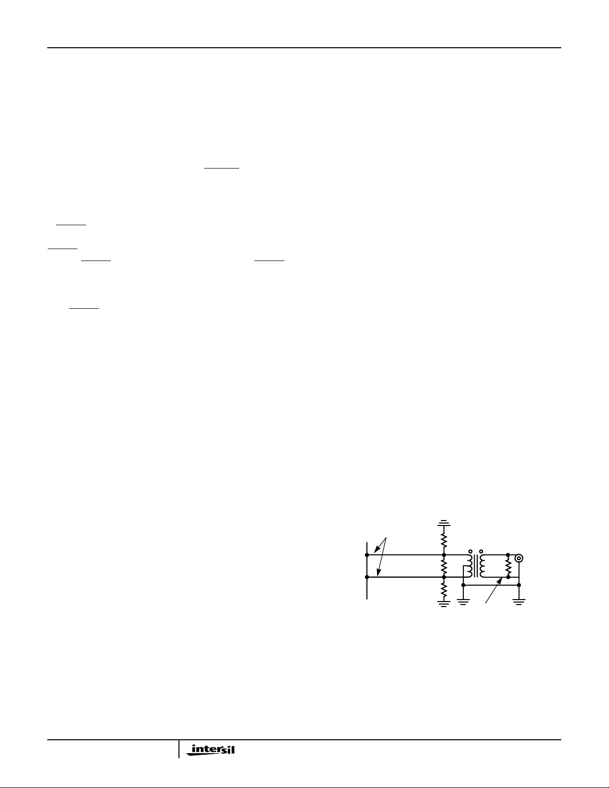
These outputs can be used in a differential-to-single-ended
arrangement. This is typically done to achieve better
harmonic rejection. Because of a mismatch in IOUTA and
IOUTB, the transformer does not improve the harmonic
rejection. However, it can provide voltage gain without
adding distortion. The SFDR measurements in this data
sheet were performed with a 1:1 transformer on the output of
the DDS (see Figure 1). With the center tap grounded, the
output swing of pins 17 and 18 will be biased at zero volts.
The loading as shown in Figure 1 will result in a 500mV
signal at the output of the transformer if the full scale output
current of the DAC is set to 20mA.
REQ IS THE IMPEDANCE
LOADING EACH OUTPUT
IOUTB
IOUTA
OUTxREQ
, where REQis ~12.5Ω. Allowing the
HSP45314
V
OUT
PIN 17
PIN 18
=2xI
center tap to float will result in identical transformer output,
however the output pins of the DAC will have positive DC
offset, which could limit the voltage swing available due to
the output voltage compliance range. The 50Ω load on the
output of the transformer represents the load at the end of a
(the impedance loading
LOAD
50Ω
100Ω
50Ω
FIGURE 1.
V
OUT
50Ω REPRESENTS THE
SPECTRUM ANALYZER
= (2 x I
50Ω
OUT
PP
x REQ)V
PP
3-4

HSP45314
‘transmission line’, typically a spectrum analyzer,
oscilloscope, or the next function in the signal chain. The
necessity to have a 50Ωimpedance looking back into the
transformer is negated if the DDS is only driving a short
trace. The output voltage compliance range does limit the
impedance that is loading the DDS output.
Ground Plane Considerations
Separate digital and analog ground planes should be used.
All of the digital functions of the device and their
corresponding components should be located over the
digital ground plane and terminated to the digital ground
plane. The same is true for the analog components and the
analog ground plane. Pins 11 through 24 are analog pins,
while all of the others are digital.
Noise Reduction Considerations
To minimize power supply noise, 0.1µF capacitors should be
placed as close as possible to the power supply pins, AV
and DVDD. Also, the layout should be designed using
separate digital and analog ground planes and these
capacitors should be terminated to the digital ground for
DV
and to the analog ground forAVDD. Additional filtering
DD
of the power supplies on the board is recommended.
DD
Power Supplies
The DDS will provide the best SFDR (Spurious Free
Dynamic Range) when using +5V analog and +5V digital
power supply. The analog supply must be +5V (±10%). The
digital supply can be either a +3.3V (±10%) or a +5V (±10%)
supply, or anything in between. The DDS is rated to
125MSPS when using a +5V digital supply. The maximum
clock is 100MSPS when using a +3.3V digital supply.
Improving SFDR
As was previously noted, using +5V power supplies provides
the best SFDR. Under some clock and output frequency
combinations, particularly when the f
than 4, the user can improve SFDR even further by
connecting the COMP2 pin (19) of the DDS to the analog
power supply. The digital supply must be +5V if this option is
explored. Improvements as much as 6dBc in the SFDR-toNyquist measurement were seen in the lab.
CLK/fOUT
ratio is less
FSK Modulation
BFSK (Binary Frequency Shift Keying) can be done by
enabling and disabling the offset frequency (ENOFR pin).
Once the offset frequency has been written once, it can be
toggled with a latency of 14 CLK cycles.
M-ary FSK or GFSK can be done by continuously loading in
new frequency words.
Quadrature Local Oscillators
Two HSP45314s can be used as sine/cosine generators for
quadrature local oscillator applications.Itisimportant to note
that the Phase Accumulator feedback needs to be zeroed in
both devices if it is desired that both DDSs restart with a
known phase, which is determined by the use of the phase
control pins, PH1 and PH0. To zero the phase accumulator,
pull bit 5 of address 13 low and then high again at the same
time in both devices.
3-5
 Loading...