Intersil Corporation HSP45256-883 Datasheet

HSP45256/883
February 1998
Features
• This Circuit is Processed in Accordance to MIL-STD883 and is Fully Conformant Under the Provisions of
Paragraph 1.2.1.
• Reconfigurable 256 Stage Binary Correlator
• 1-Bit Reference x 1, 2, 4, or 8-Bit Data
• Separate Control and Reference Interfaces
• Configurable for 1-D and 2-D Operation
• Double Buffered Mask and Reference
• Programmable Output Delay
• Cascadable
• Standard Microprocessor Interface
Applications
• Radar/Sonar
• Spread Spectrum Communications
• Pattern/Character Recognition
• Error Correction Coding
Ordering Information
TEMP.
PART NUMBER
HSP45256GM-20/883 -55 to 125 85 Ld PGA
HSP45256GM-25/883 -55 to 125 85 Ld PGA
RANGE (oC) PACKAGE
PKG.
NO.
Binary Correlator
Description
The Intersil HSP45256/883 is a high-speed, 256 tap binary
correlator. It can be configured to perform one-dimensional
or two-dimensional correlations of selectable data precision
and length. Multiple HSP45256’s can be cascaded for
increased correlation length. Unused taps can be masked
out for reduced correlation length.
The correlation array consists of eight 32-tap stages. These
may be cascaded internally to compare 1, 2, 4 or 8-bit input
data with a 1-bit reference. Depending on the number of bits
in the input data, the length of the correlation can be up to
256, 128, 64, or 32 taps. The HSP45256 can also be
configured as two separate correlators with window sizes
from 4 by 32 to 1 by 128 each. The Mask Register can be
used to prevent any subset of the 256 bits from contributing
to the correlation score.
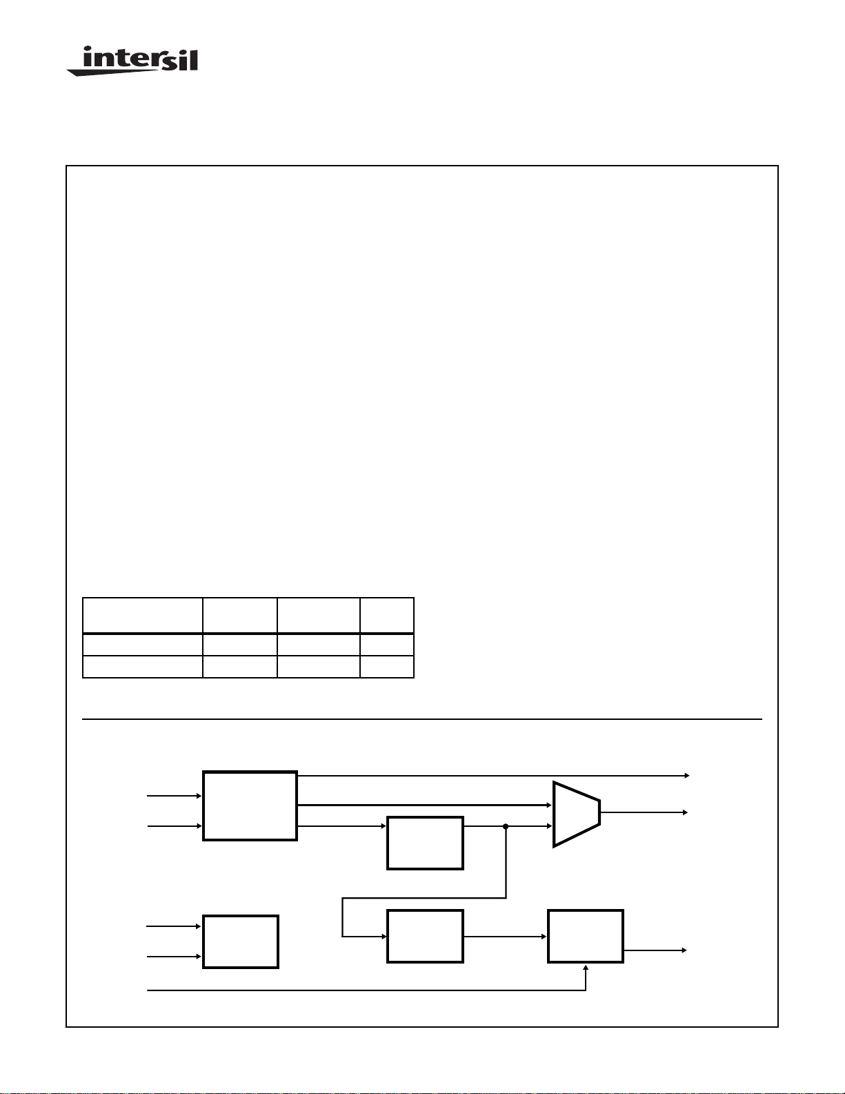
The9- output of the correlation array (correlation score)
feeds the weight and sum logic, which gives added flexibility
to the data format. In addition, an offset register is provided
so that a preprogrammed value can be added to the correlation score. This result is then passed through a user programmable delay stage to the cascade summer. The delay
stage simplifies the cascading of multiple correlators by
compensating for the latency of previous correlators.
The Binary Correlator is configured by writing a set of control
registers via a standard microprocessor interface. To simplify
operation, both the Control and Reference Registers are
double buffered. This allows the user to load new mask and
reference data while the current correlation is in progress.
Block Diagram
DIN0-7
DREF0-7
DCONT0-7
A0-2
CASIN0-12
CAUTION: These devices are sensitive to electrostatic discharge; follow proper IC Handling Procedures.
http://www.intersil.com or 407-727-9207
256 TAP
CORRELATION
ARRAY
CONTROL
| Copyright © Intersil Corporation 1999
WEIGHT
AND SUM
DELAY
9-38
MUX
CASCADE
SUMMER
DOUT0-7
AUXOUT0-8
CASOUT0-12
File Number 2997.3

HSP45256/883
Pinouts
2173456 891011
A
2 4 5 7 10 11
CASIN
CASIN CASIN
B
C
D
E
F
G
H
J
K
L
CASIN
GND
CASIN INDEX
CLK
DIN7
DIN4 DIN6
DREF
DIN0
DREF
DREF
DREF
DREF
08
PIN
V
CC
DIN5
DIN3 DIN2
6
DREF
DIN1
7
DREF
5
4
DREF
1
3
V
CC
2
0
TXFRGND
R C DCONT
LOADLOAD
A2
85 PIN PGA
TOP VIEW
CASIN CASINCASIN CASIN CASIN CASIN
CAS CAS CAS CAS CAS CAS
OUT2OUT1OUT4OUT6OUT7OUT
9631
CASIN
CASIN
A1
A0
12
54
62
85 PIN PGA
BOTTOM VIEW
OUT0OUT3OUT
OEC
DOUT0 DOUT1 DOUT2
DOUT
DCONTDCONT
DCONT
DCONT
DCONTDCONTDCONT
OEA
0317
CASCASCAS CAS
5
GND
OUT
8
10
CAS CAS
OUT9OUT
GND
DOUT DOUT
DOUT DOUT
V
CC
AUX AUX
OUT1OUT
GND
AUX
AUX AUX
OUT
OUT
6
OUT8OUT7OUT
11
CAS
OUT
12
734
65
0
AUX
OUT
2
OUT
3
4
AUXAUXAUX
5
L
DREF0 GND TXFR A2 DCONT DCONT DCONT0
K
DREF2 A0 DCONT
J
DREF3
H
DREF5
G
F
DREF6
E
D
C
B
A
CASIN CASIN CASIN
V
RLOAD CLOAD
CC
DREF1
DREF4 AUXOUT AUXOUT
DIN0 DREF7 DIN1
DIN3 DIN2
DIN5
DIN7
CLK CASIN0 CASIN CASIN
GND
CC
INDEX
PIN
CASIN6CASIN1 CASINCASIN3
245 7
1234 567 89 1011
71
A1 DCONT DCONT GND
812
CASOUT
9
10
DCONT
6
5
2
CASINCASINCASIN
11
DCONT
3
2
4
OEC
CASOUT
1
CASOUT
0
OEA
CASOUT
4
CASOUT
3
AUXOUT8AUXOUT7AUXOUT
6
V
CC
DOUT4
DOUT0 DOUT1 DOUT2DIN4 DIN6
6
5
AUXOUT
4
DOUT6 DOUT5
DOUT7 DOUT3
GNDV
CASOUT
9
CASOUT
7
GND
AUXOUT
CASOUT
CASOUT
5
AUXOUT
3
AUXOUT
2
01
CASOUT
12
CASOUT
11
CASOUT
10
CASOUT
8
9-39

HSP45256/883
Pin Description
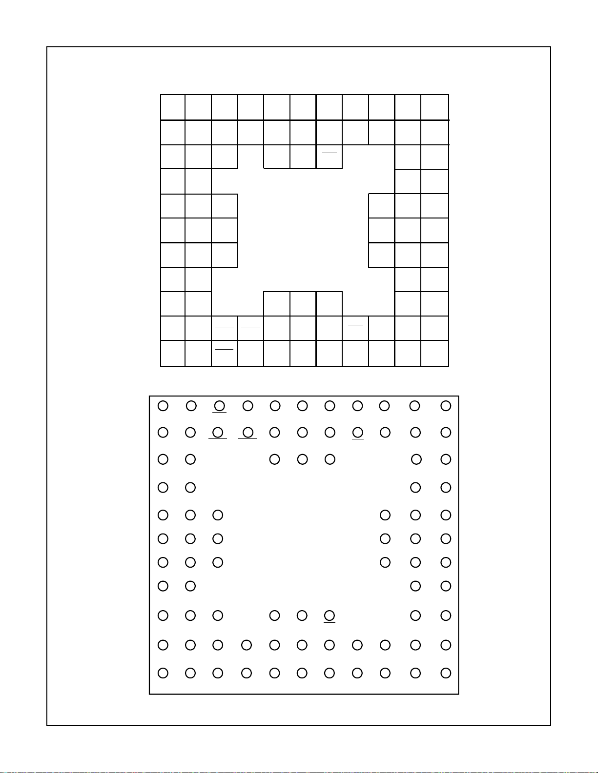
SYMBOL PIN NUMBER TYPE DESCRIPTION
V
CC
GND A10, B1, D10,
DIN0-7 D1, E1-E3, F2,
DOUT0-7 E9-E11, F9-F11,
CLK C1 I System Clock. Positive edge triggered.
CASIN0-12 A1-A6, B2-B5,
CASOUT0-12 A7-A9, A11,
OEC C7 I OEC is the output enable for CASOUT0-12. When OEC is high, the output is three-stat-
TXFR L3 I TXFR is a synchronous clock enable signal that allows the loading of the reference and
DREF0-7 F1, G2, H1, H2,
RLOAD K3 I RLOAD enables loading of the reference registers. Data on DREF0-7 is loaded into the
DCONT0-7 J6, J7, K6, K7,
CLOAD# K4 I CLOAD enables the loading of the data on DCONT0-7. The destination of this data is
A0-2 J5, K5, L4 I A0-2 is a 3-bit address that determines what function will be performed when CLOAD
AUXOUT0-8 H10, H11, J11,
OEA K8 I The OEA signal is the output enable for the AUXOUT0-8 output. WhenOEA is high, the
Index Pin C3 Used for orienting pin in socket or printed circuit board. Must be left as a no connect in
D2, G9, K2 The +5V power supply pin.
Ground.
J10, L2
I The DIN0-7 bus consists of eight single data input pins. The assignment of the active
F3, G1, G3
O The DOUT0-7 bus is the data output of the correlation array. The format of the output
G10, G11
C2, C5, C6
O CASOUT0-12 is the output correlation score. This value is the delayed sum of all the
B6-B11, C10,
C11, D11
J1, J2, K1, L1
L5-L8
O AUXOUT0-8 is a 9-bit bus that provides either the data reference output or the 9-bit
K9-K11, L9-L11
pins is determined by the configuration. Data is loaded synchronous to the rising edge
of CLK. DIN0 is the LSB.
is dependent on the window configuration and bit weighting. DOUT0 is the LSB.
I CASIN0-12 allows multiple correlators to be cascaded by connecting CASOUT0-12 of
one correlator to CASIN0-12 of another. The CASIN bus is added internally to the
correlation score to form CASOUT. CASIN0 is the LSB.
256 taps of one chip and CASIN0-12. When the part is configured to act as two
independent correlators, CASOUT0-8 represents the correlation score for the first
correlator while the second correlation score is available on the AUXOUT0-8 bus. In
this configuration, the cascading feature is no longer an option. CASOUT0 is the LSB.
ed. Processing is not interrupted by this pin (active low).
mask inputs from the preload register to the correlation array. Data is transferred on the
rising edge of CLK while TXFR is low (active low).
I DREF0-7 is an 8-bit wide data reference input. This is the input data bus used to load
the reference data. RLOAD going active initiates the loading of the reference registers.
This input bus is used to load the reference registers of the correlation array. The manner in which the reference data is loaded is determined by the window configuration. If
the window configuration is 1 x 256, the reference bits are loaded one at a time over
DREF7. When the HSP45256 is configured as an 8 x 32 array, the data is loaded into
all stages in parallel. In this case, DREF7 is the reference data for the first stage and
DREF0 is the reference data for the eighth stage. The contents of the reference data
registers are not affected by changing the window configuration. DREF0 is the LSB.
preload registers on the rising edge of RLOAD. This data is transferred into the correlation array by TXFR (active low).
I DCONT0-7 is the control data input, which is used to load the mask bit for each tap as
well as the configuration registers. The mask data is sequentially loaded into the eight
stages in the same manner as the reference data. DCONT0 is the LSB.
controlled by A0-2 (active low).
is active. This address bus is set up with respect to the rising edge of the load signal,
CLOAD. A0 is the LSB.
correlation score of the second correlator, depending on the configuration. When the
user programs the chip to be two separate correlators, the score of the second correlator is output on this bus. When the user has programmed the chip to be one correlator,
AUXOUT0-7 represents the reference data out, with the state of AUXOUT0-8
undefined. AUXOUT0 is the LSB.
output is disabled. Processing is not interrupted by this pin (active low).
circuit.
9-40
 Loading...