

Intersil Corporation HSP45256 Datasheet
HSP45256
Data Sheet May 1999 File Number
Binary Correlator
The Intersil HSP45256 is a high-speed, 256 tap binary
correlator. It can be configured to perform one-dimensional
or two-dimensional correlations of selectable data precision
and length. Multiple HSP45256’s can be cascaded for
increased correlation length. Unused taps can be masked
out for reduced correlation length.
The correlation array consists of eight 32-tap stages. These
may be cascaded internally to compare 1, 2, 4 or 8-bit input
data with a 1-bit reference. Depending on the numberofbits
in the input data, the length of the correlation can be up to
256, 128, 64, or 32 taps. The HSP45256 can also be
configured as two separate correlators with window sizes
from 4 by 32 to 1 by 128 each. The mask register can be
used to prevent any subset of the 256 bits from contributing
to the correlation score.
The output of the correlation array (correlation score) feeds
the weight and sum logic, which gives added flexibilitytothe
data format. In addition, an offset register is providedsothat
a preprogrammed value can be added to the correlation
score. This result is then passed through a user
programmable delay stage to the cascade summer. The
delay stage simplifies the cascading of multiple correlators
by compensating for the latency of previous correlators.
The Binary Correlatorisconfigured by writing a set of control
registers via a standard microprocessor interface. Tosimplify
operation, both the control and reference registers are
double buffered. This allows the user to load new mask and
reference data while the current correlation is in progress.
2814.4
Features
• Reconfigurable 256 Stage Binary Correlator
• 1-Bit Reference x 1, 2, 4, or 8-Bit Data
• Separate Control and Reference Interfaces
• 25.6, 33MHz Versions
• Configurable for 1-D and 2-D Operation
• Double Buffered Mask and Reference
• Programmable Output Delay
• Cascadable
• Standard Microprocessor Interface
Applications
• Radar/Sonar
• Spread Spectrum Communications
• Pattern/Character Recognition
- Error Correction Coding
Ordering Information
TEMP.
PART NUMBER
HSP45256JC-25 0 to 70 84 Ld PLCC N84.1.15
HSP45256JC-33 0 to 70 84 Ld PLCC N84.1.15
HSP45256GC-25 0 to 70 85 Ld PGA G85.A
HSP45256GC-33 0 to 70 85 Ld PGA G85.A
HSP45256JI-25 -40 to 85 84 Ld PLCC N84.1.15
HSP45256JI-33 -40 to 85 84 Ld PLCC N84.1.15
RANGE (oC) PACKAGE
PKG.
NO.
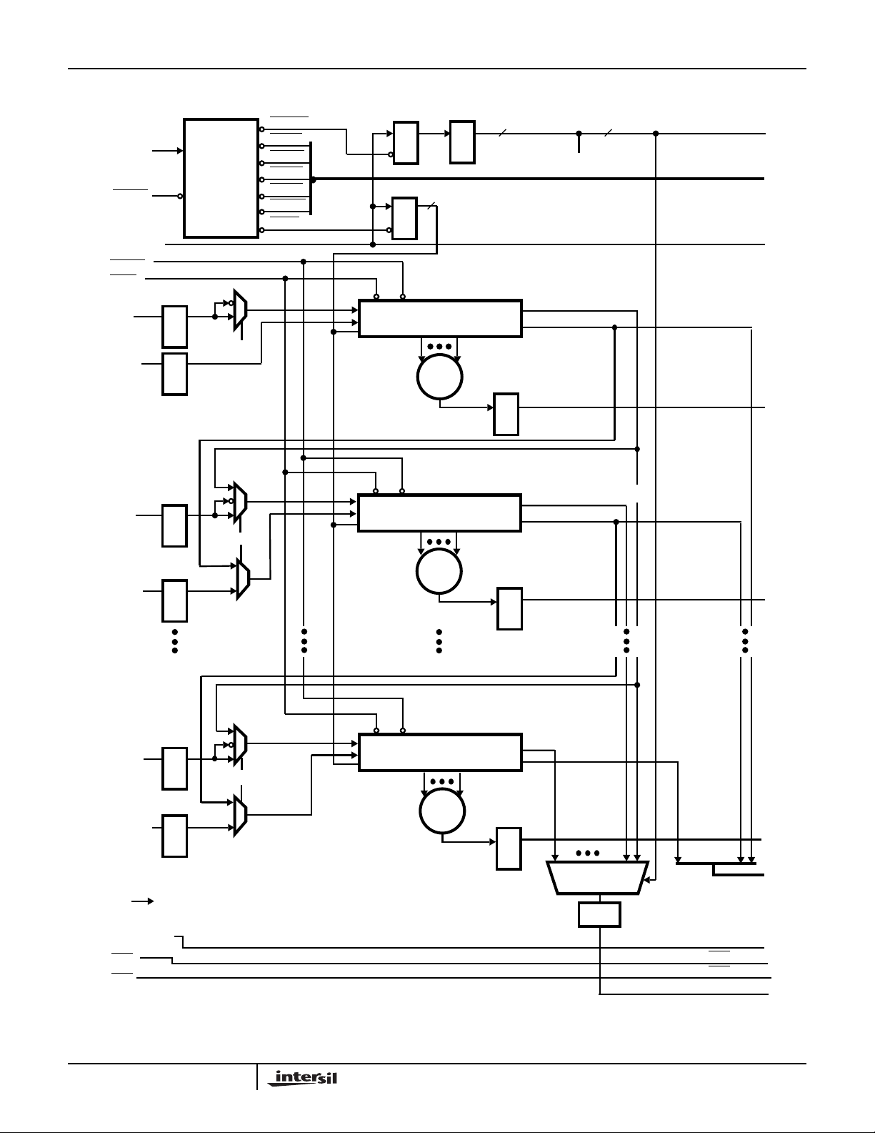
Block Diagram
DIN0-7
DREF0-7
DCONT0-7
A0-2
CASIN0-12
256 TAP
CORRELATION
ARRAY
CONTROL
1
DOUT
DREFOUT
CSCORE
WEIGHT
AND SUM
DELAY
CAUTION: These devices are sensitive to electrostatic discharge; follow proper IC Handling Procedures.
http://www.intersil.com or 407-727-9207
MUX
CASCADE
SUMMER
| Copyright © Intersil Corporation 1999
DOUT0-7
AUXOUT0-8
CASOUT0-12
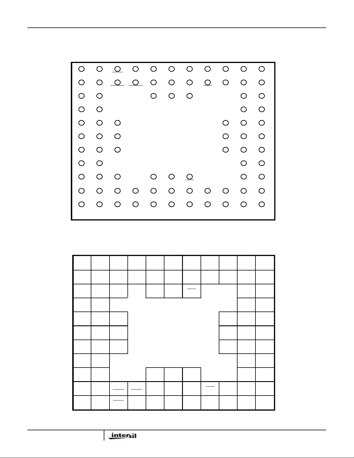
Pinouts
HSP45256
85 PIN PGA
BOTTOM VIEW
L
DREF0 GND
K
DREF2 A0 DCONTDCONTRLOAD CLOAD
J
H
DREF4 AUXOUT AUXOUTDREF5
G
DIN0 DREF7 DIN1 DOUT6 DOUT5
F
DIN3 DIN2 DOUT4DREF6 DOUT7 DOUT3
E
D
C
CLK CASIN0 CASIN CASIN OEC CASOUT
B
A
2457
1234567891011
TXFR A2 DCONT7 DCONT1 DCONT0DCONT3 AUX AUX AUX
V
CC
A1 DCONT DCONT GNDDREF1DREF3
V
CC
PIN 8 12
CASIN6CASIN1 CASINCASIN3GND CASOUT
10
62
54
CASOUT
CASOUT
29
CASINCASINCASINCASIN CASIN CASIN GND CASOUT
11
1
CASOUTCASOUT
0
OUT8 OUT7 OUT5
OEA
OUT6 OUT4
V
CC
DOUT0 DOUT1 DOUT2DIN4 DIN6DIN5
4
CASOUT
3
5
AUXAUX
GNDDIN7 CASOUT
CASOUTINDEX
9
CASOUTCASOUTCASOUT
7
AUX
OUT3
AUX
OUT2
01
12
11
10
8
85 PIN PGA
TOP VIEW
2173 4 5 6 8 9 10 11
2
GND
CLK
DIN7
DIN4
DREF
6
DIN0
DREF
5
DREF
3
DREF
2
DREF
0
CASIN
CASIN
CASIN
DREF
DREF
DREF
CASIN
A
B
C
D
E
F
G
H
J
K
L
4
1
0
V
CC
DIN5
DIN3
7
4
1
V
CC
GND
CASIN
CASIN
INDEX
5
3
PIN
DIN6
DIN2
DIN1
R
LOAD
TXFR
CASIN
CASIN
LOAD
A2
CASIN
7
CASIN
6
CASIN
C
DCONT
10
A1
A0
CASIN
CAS
9
OUT2
CASIN
8
DCONT
DCONT
DCONT
7
CAS
OUT
11
CAS
OUT1
OEC
12
DCONT
5
DCONT
6
DCONT
1
CAS
OUT3
CAS
OUT4
4
OEA
2
DCONT
3
CAS
OUT5
CAS
OUT6
DOUT0
DOUT
V
AUX
OUT6
AUX
0
OUT8
4
CC
GND
CAS
OUT7
CAS
OUT9
GND
DOUT
DOUT
DOUT
AUX
OUT1
GND
AUX
OUT4
AUX
OUT7
CAS
OUT8
CAS
OUT10
CAS
OUT11
CAS
OUT12
DOUT2
DOUT
7
6
3
DOUT
5
AUX
OUT0
AUX
OUT2
AUX
OUT3
AUX
OUT5
2
HSP45256
Pinouts
(Continued)
CASIN1
CASIN0
GND
CLK
V
DIN7
DIN6
DIN5
DIN4
DIN3
DIN2
DIN1
DIN0
DREF7
DREF6
DREF5
DREF4
DREF3
DREF2
DREF1
DREF0
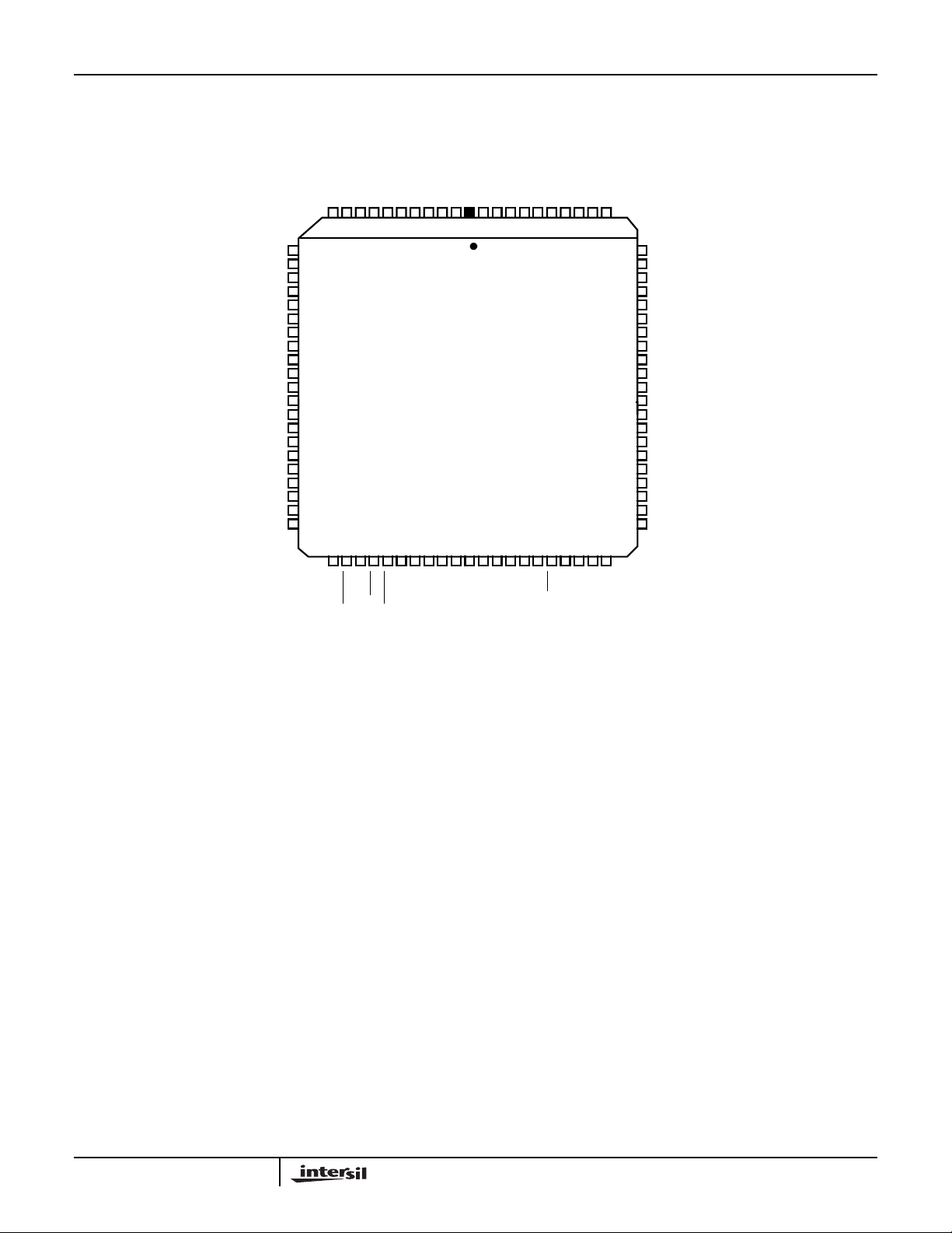
84 PIN PLCC
TOP VIEW
CASIN2
CASIN3
CASIN4
CASIN5
CASIN6
CASIN7
CASIN8
CASIN9
CASIN10
CASIN11
CASIN12
OEC#
CASOUT0
CASOUT1
CASOUT2
CASOUT3
CASOUT4
CASOUT5
GND
CASOUT7
CASOUT6
111098765432184838281807978777675
12
13
14
15
16
CC
17
18
19
20
21
22
23
24
25
26
27
28
29
30
31
32
33 34 35 36 37 38 39 40 41 42 43 44 45 46 47 48 49 50 51 52 53
74
73
72
71
70
69
68
67
66
65
64
63
62
61
60
59
58
57
56
55
54
CASOUT8
CASOUT9
CASOUT10
CASOUT11
GND
CASOUT12
DOUT0
DOUT1
DOUT2
DOUT3
DOUT4
V
CC
DOUT5
DOUT6
DOUT7
AUXOUT0
AUXOUT1
AUXOUT2
AUXOUT3
GND
AUXOUT4
GND
TXFR
CLOAD
A2A1A0
DCONT7
DCONT6
DCONT5
DCONT4
DCONT3
DCONT2
DCONT1
DCONT0
OEA
AUXOUT8
AUXOUT7
AUXOUT5
AUXOUT6
CC
V
RLOAD
3
HSP45256
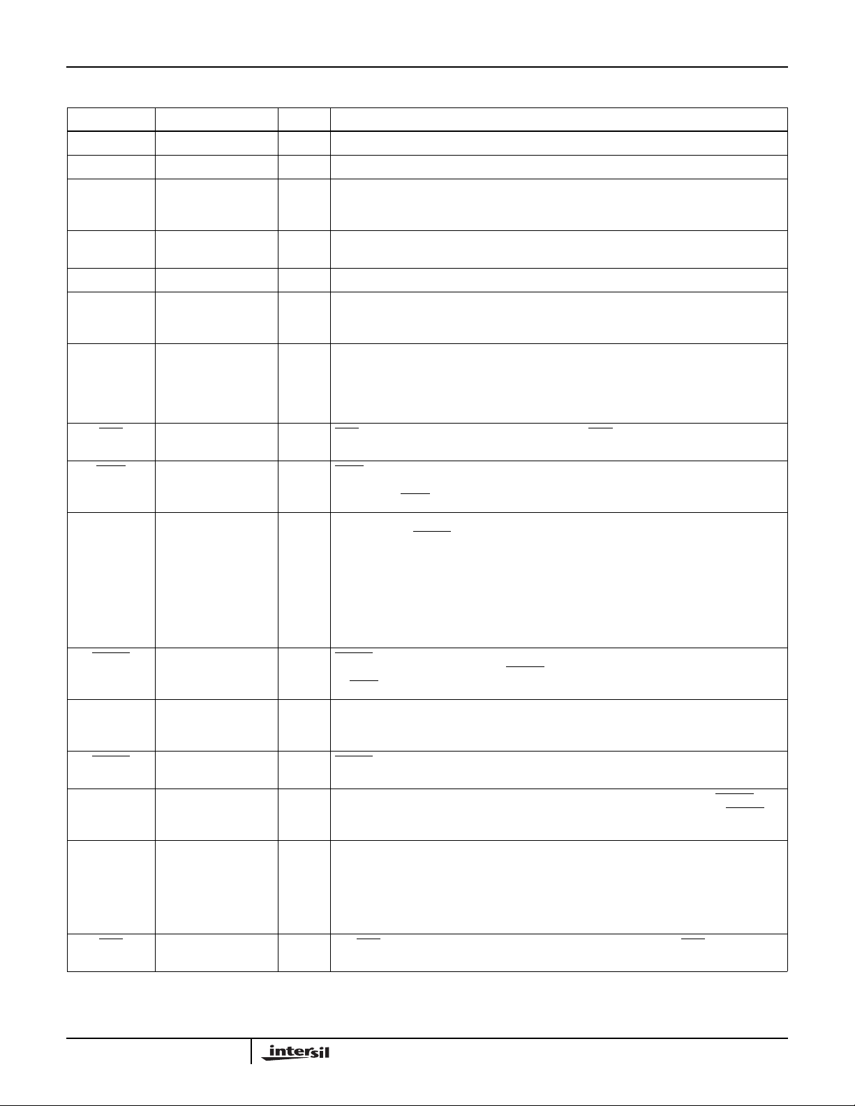
Pin Descriptions
SYMBOL PLCC PIN NUMBER TYPE DESCRIPTION
V
CC
GND 14, 35, 55, 70, 77 Ground.
DIN0-7 17-24 I The DIN0-7 bus consists of eight single data input pins. The assignment of the active pins is
DOUT0-7 60-62, 64-68 O The DOUT0-7 bus is the data output of the correlation array.The format of the output is de-
CLK 15 I System Clock. Positive edge triggered.
CASIN0-12 1-13 I CASIN0-12 allows multiple correlators to be cascaded by connecting CASOUT0-12 of one
CASOUT0-12 69, 71-76, 78-83 O CASOUT0-12 is the output correlation score. This value is the delayed sum of all the 256
OEC 84 I OEC is the output enable for CASOUT0-12. When OEC is high, the output is three-stated.
TXFR 36 I TXFR is a synchronous clock enable signal that allows the loading ofthe referenceandmask
DREF0-7 25-32 I DREF0-7 is an 8-bit wide data reference input. This is the input data bus used to load the
RLOAD 34 I RLOADenables loading of the reference registers. Data on DREF0-7 is loaded into the pre-
DCONT0-7 41-48 I DCONT0-7 is the control data input which is used to load the mask bit for each tap, as well
CLOAD 37 I CLOAD enables the loading of the data on DCONT0-7. The destination of this data is con-
A0-2 38-40 I A0-2 is a 3-bit address that determines what function will be performed when CLOAD is ac-
AUXOUT0-8 50-54, 56-59 O AUXOUT0-8 is a 9-bit bus that provides either the data reference output in the single corre-
OEA 49 I The OEA signal is the output enable for the AUXOUT0-8 output. When OEA is high, the out-
16, 33, 63 The +5V power supply pin.
determined by the configuration. Data is loaded synchronous to the rising edge of CLK. DIN0
is the LSB.
pendent on the window configuration and bit weighting. DOUT0 is the LSB.
correlator to CASIN0-12 of another. The CASIN bus is added internally to the correlation
score to form CASOUT. CASIN0 is the LSB.
taps of one chip and CASIN0-12. When the part is configured to act as two independent correlators, CASOUT0-8 represents the correlation score for the first correlator while the second correlation score is available on the AUXOUT0-8 bus. In this configuration, the
cascading feature is no longer an option. CASOUT0 is the LSB.
Processing is not interrupted by this pin (active low).
inputs from the preload register to the correlation array.Data is transferredonthe rising edge
of CLK while TXFR is low (active low).
reference data. RLOAD going active initiates the loading of the reference registers. This input bus is used to load the reference registers of the correlation array.The manner in which
the reference data is loaded is determined by the window configuration. If the window configuration is 1 x 256, the reference bits are loaded one at a time over DREF7. When the
HSP45256 is configured as an8x32array,thedata is loaded into all stages in parallel. In
this case, DREF7 is the reference data for the first stage and DREF0 is the reference data
for the eighth stage. The contents of the reference data registers are not affected by changing the window configuration. DREF0 is the LSB.
load registers on the rising edge of RLOAD. This data is transferred into the correlation array
by TXFR (active low).
as the configuration registers. The mask data is sequentially loaded into the eight stages in
the same manner as the reference data. DCONT0 is the LSB.
trolled by A0-2 (active low).
tive.This address bus is set up with respect to the rising edge of the load signal, CLOAD. A0
is the LSB.
lation configuration or the 9-bit correlation score of the second correlator, in the dual correlator configuration. When the user programs the chip to be two separate correlators, the
score of the second correlator is output on this bus. When the user has programmed the chip
to be one correlator, AUXOUT0-7 represents the reference data out, with the state of
AUXOUT8 undefined. AUXOUT0 is the LSB.
put is disabled. Processing is not interrupted by this pin (active low).
4
Block Diagram
HSP45256
A(2:0)
CLOAD
DCONT(7:0)
RLOAD
TXFR
DIN7
DREF7
DIN6
DREF6
>
>
>
>
R
E
G
R
E
G
R
E
G
R
E
G
DECODE
TC
DO7
CONFIG(4:0)
RO7
CONFIG
OFFAL
OFFAM
DELAY
OFFBL
OFFBM
MASK
(001)
R
E
G
>
(000)
8
R
E
G
>
32 TAP CORRELATOR STAGE
MR7
32 TAP CORRELATOR STAGE
MR6
6 CONFIG(4:0)
R
E
G
>
DO7
RO7
+
R
E
G
>
DO6
RO6
5
TC
DATA OUT
RO7
CORRELATION
SCORE OUT
CO7
DATA OUT
RO6
+
R
E
G
>
CO6
DO1
DIN0
DREF0
CLK
CASIN(12:0)
OEA
OEC
R
E
G
R
E
G
CONFIG(4:0)
RO1
>
>
32 TAP CORRELATOR STAGE
MR0
NOTE: All registers clocked with CLK unless otherwise specified.
CORRELATOR BLOCK DIAGRAM
5
DO0
RO0
RO0
+
R
E
G
>
MUX
ARRAY
>
G
E
R
CO0
REFERENCE OUT
CASIN(12:0)
OEA
OEC
DOUT(7:0)
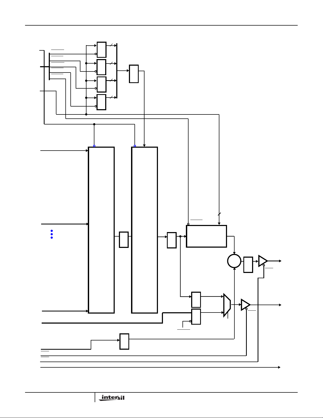
HSP45256
Block Diagram
OFFSET
REGISTER A
OFFAM
OFFAL
OFFBM
OFFBL
DELAY
CONFIG(4:0)
CORRELATION
SCORE OUT
CO7
(Continued)
(010)
(011)
(101)
(110)
R
E
G
>
R
E
G
>
R
E
G
>
R
E
G
>
5
8
1
8
OFFSET
REGISTER B
R
E
G
>
CO6
CO0
REFERENCE OUT
CASIN(12:0)
OEA
OEC
DOUT(7:0)
WEIGHT
CASCADE
REGISTER
4
DELAY
R
E
G
>
R
E
G
>
SUM
R
E
G
>
RO(0-7)
PROGRAMMABLE
>
>
RLOAD
R
E
G
R
E
G
DELAY
(100)
CONFIG(4:0)
CASOUT(12:0)
R
+
E
G
>
OEA
OEC
AUXOUT(8:0)
DOUT(7:0)
NOTE: All registers clocked with CLK unless otherwise specified.
6
HSP45256
Functional Description
The correlation array consists of eight 32-bit stages. The first
stage receives data directly from input pin DIN7. The other
seven stages receive input data from either an external data
pin, DIN0-6, or from the Shift Register output of the previous
stage, as determined by the Configuration Register. When
the part is configured as a single correlator the sum of
correlation score, Offset Register and cascade input
appears on CASOUT0-12. Delayed versions of the data and
reference inputs appear on DOUT0-7 and AUXOUT0-7,
respectively. The input and output multiplexers of the
correlation array are controlled together; for example, in a 1
x 256 correlation, the input data is loaded into DIN7 and the
output appears on DOUT7. The configuration of the data
bits, the length of the correlation (and in the two-dimensional
data, the number of rows), is commonly called the
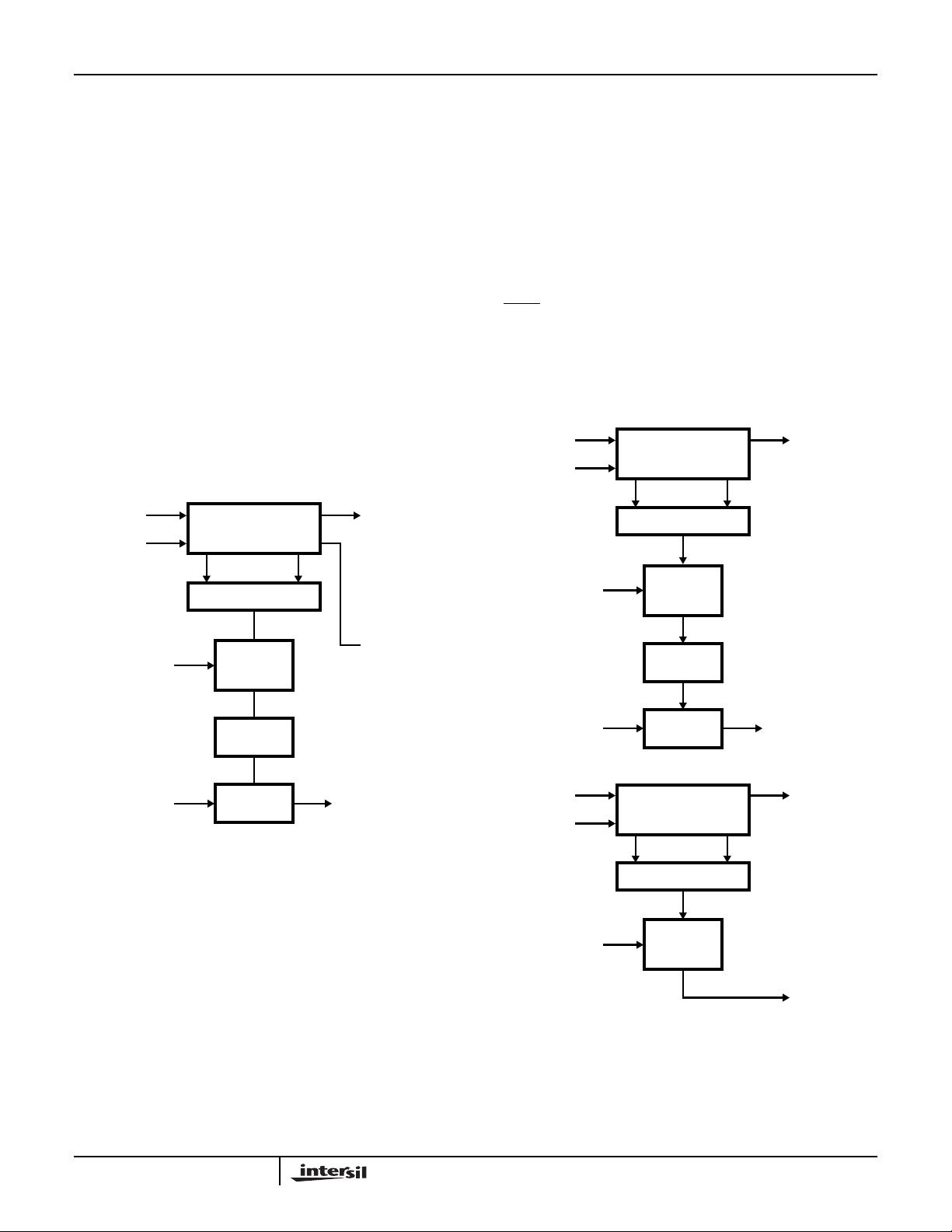
correlation window. A top level Block Diagram of the single
correlator configuration is shown in Figure 1. Compare the
single correlator configuration data output and correlation
output to the top level Block Diagram of the dual correlator
configuration shown in Figure 2.
DIN(7:0)
DREF(7:0)
OFFA
8 32-BIT
CORRELATORS
• • • • • • • • • • • •
SUM
CORR SCORE
WEIGHT
AND
SUM
DOUT(7:0)
AUXOUT(7:0)
Correlator Array
The core of the HSP45256 is the correlation array, which
consists of eight 32-tap stages. A single correlator cell
consists of an XNOR gate for the individual bit comparison;
i.e., if the data and reference bits are either both high or both
low, the output of the correlator cell is high. Figure 3 details
the circuitry of a single correlation cell and Figure 4 shows
the timing for that single correlation cell. In addition, two
latches, one for the reference and one for the control data
path are contained in this cell. These latches are loaded
from the Preload Registers on the rising edge of CLK when
TXFR is low so that the reference and mask values are
updated without interrupting data processing.
The mask function is implemented with an AND gate. When
a mask bit is a logic low, the corresponding correlator cell
output is low.
DIN(7:4)
DREF(7:4)
OFFA
4 32-BIT
CORRELATORS
• • • • • • • • • • • •
SUM
CORR SCORE
WEIGHT
AND
SUM
DELAY
= 0000
DOUT(7:4)
DELAY
CASIN(12:0) CASOUT(12:0)
FIGURE 1. SINGLE CORRELATOR CONFIGURATION
SUM
7
CASIN(12:0)
DIN(3:0) DOUT (3:0)
DREF(3:0)
OFFB
FIGURE 2. DUAL CORRELATOR CONFIGURATION
SUM
CORRELATOR #1
4 32-BIT
CORRELATOR
• • • • • • • • • • • •
SUM
CORR SCORE
WEIGHT
AND
SUM
CORRELATOR #2
CASOUT(8:0)
AUXOUT(8:0)
 Loading...