Intersil Corporation HSP45240-883 Datasheet

HSP45240/883
February 1998
Features
• This Circuit is Processed in Accordance to MIL-STD883 and is Fully Conformant Under the Provisions of
Paragraph 1.2.1.
• Block Oriented 24-Bit Sequencer
• Configurable as Two Independent 12-Bit Sequencers
• 24 x 24 Crosspoint Switch
• Programmable Delay on 12 Outputs 9-
• Multi-Chip Synchronization Signals
• Standard µP Interface
• 100pF Drive on Outputs
• DC to 40MHz Clock Rate
Applications
• 1-D, 2-D Filtering
• Pan/Zoom Addressing
• FFT Processing
• Matrix Math Operations
Address Sequencer
Description
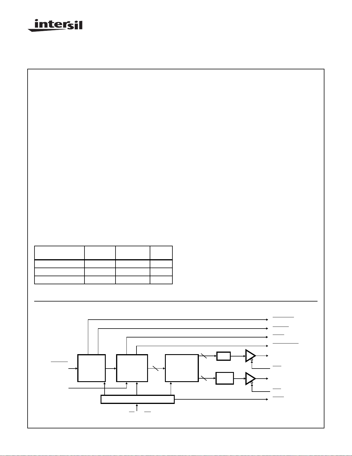
The Intersil HSP45240/883 is a high speed Address
Sequencer which provides specialized addressing for functions like FFTs, 1-D and 2-D filtering, matrix operations, and
image manipulation. The sequencer supports block oriented
addressing of large data sets up to 24 bits at clock speeds
up to 40MHz.
Specialized addressing requirements are met by using the
onboard 24 x 24 crosspoint switch. This feature allows the
mapping of the 24 address bits at the output of the address
generator to the 24 address outputs of the chip. As a result,
bit reverse addressing, such as that used in FFTs, is made
possible.
A single chip solution to read/write addressing is also made
possible by configuring the HSP45240 as two 12-bit
sequencers. To compensate for system pipeline delay, a programmable delay is provided on 12 of the address outputs.
The HSP45240 is manufactured using an advanced CMOS
process, and is a low power fully static design. The configuration of the device is controlled through a standard microprocessor interface and all inputs/outputs, with the e xception
of clock, are TTL compatible.
Ordering Information
TEMP.
PART NUMBER
HSP45240GM-25/883 -55 to 125 68 Ld PGA
HSP45240GM-33/883 -55 to 125 68 Ld PGA
HSP45240GM-40/883 -55 to 125 68 Ld PGA
RANGE (oC) PACKAGE
Block Diagram
STARTIN
DLYBLK
START
CIRCUITRY
SEQUENCE
GENERATOR
PROCESSOR INTERFACE
PKG.
NO.
24
CROSS-POINT
SWITCH
STARTOUT
ADDVAL
DONE
BLOCKDONE
12
REG
12
DELAY
1-8
OUT12-23
OEH
OUT0-11
OEL
BUSY
CS, A0, WR
D0-6,
CAUTION: These devices are sensitive to electrostatic discharge; follow proper IC Handling Procedures.
http://www.intersil.com or 407-727-9207
| Copyright © Intersil Corporation 1999
9-16
File Number 2816.3

HSP45240/883
Absolute Maximum Ratings Thermal Information
Supply Voltage . . . . . . . . . . . . . . . . . . . . . . . . . . . . . . . . . . . . .+8.0V
Input, Output Voltage Applied. . . . . . . . . . GND -0.5V to VCC +0.5V
ESD Classification . . . . . . . . . . . . . . . . . . . . . . . . . . . . . . . . Class 1
Operating Conditions
Temperature Range . . . . . . . . . . . . . . . . . . . . . . . . . -55oC to 125oC
Voltage Range . . . . . . . . . . . . . . . . . . . . . . . . . . . . . +4.5V to +5.5V
CAUTION: Stresses above those listed in “Absolute Maximum Ratings” may cause permanent damage to the device. This is a stress only rating and operation
of the device at these or any other conditions above those indicated in the operational sections of this specification is not implied.
NOTE:
1. θJA is measured with the component mounted on an evaluation PC board in free air.
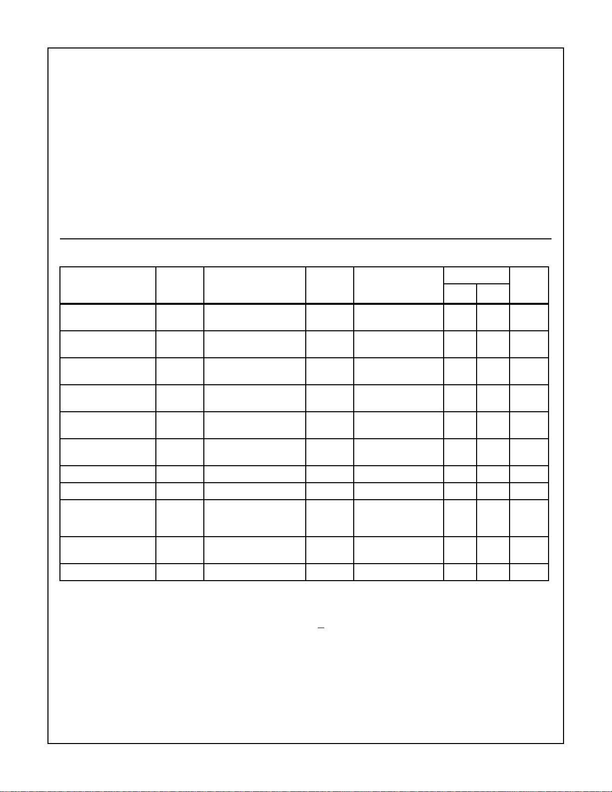
TABLE 1. DC ELECTRICAL SPECIFICATIONS
Device Guaranteed and 100% Tested
PARAMETER SYMBOL TEST CONDITIONS
Logical One Input
Voltage
Logical Zero Input
Voltage
Output HlGH Voltage V
Output LOW Voltage V
Input Leakage Current I
Output Leakage Current
Clock lnput High V
Clock Input Low V
Standby Power Supply
Current
Operating Power
Supply Current
Functional Test FT (Note 4) 7, 8 -55 ≤ TA≤ 125 - NOTES:
2. Interchanging of force and sense conditions is permitted.
3. Operating Supply Current is proportional to frequency, typical rating is 3mA/MHz.
4. Tested as follows: t = 1MHz, VIH = 2.6, VIL = 0.4, VOH≥ 1.5V, VOL< 1.5V, V
V
V
OH
VDD= 5.5V 1, 2, 3 -55 ≤ TA≤ 125 2.2 - V
lH
VDD = 4.5V 1, 2, 3 -55 ≤TA≤ 125 - 0.8 V
IL
IOH = -400µA
VDD = 4.5V (Note 2)
OL
I
VCC= 4.5V (Note 2)
VIN = VCC or GND
I
VCC= 5.5V
I
OV
VCC= 5.5V
IHC
ILC
I
CCSB
VCC= 5.5V 1, 2, 3 -55 ≤ TA≤ 125 3.0 - V
VCC= 4.5V 1, 2, 3 -55 ≤ TA≤ 125 - 0.8 V
VIN = VCC or GND
VCC= 5.5V,
Outputs Open
I
CCOP
f = 33MHz
VCC= 5.5V (Note 3)
OL = +2.0mA
= VCC or GND
OUT
Thermal Resistance (Typical, Note 1) θJA (oC/W) θJC (oC/W)
PGA Package . . . . . . . . . . . . . . . . . . . 37.1 10.1
Maximum Package Power Dissipation at 125oC
PGA Package . . . . . . . . . . . . . . . . . . . . . . . . . . . . . . . . . . . 1.35W
Maximum Junction Temperature. . . . . . . . . . . . . . . . . . . . . . . . 175oC
Maximum Storage Temperature Range . . . . . . . . . .-65oC to 150oC
Maximum Lead Temperature (Soldering 10s) . . . . . . . . . . . . .300oC
Die Characteristics
Gate Count . . . . . . . . . . . . . . . . . . . . . . . . . . . . . . . . . . . . . . . .8,388
GROUP A
SUBGROUPS TEMPERATURE (oC)
1, 2, 3 -55 ≤ TA≤ 125 2.6 - V
1, 2, 3 -55 ≤ TA≤ 125 - 0.4 V
1, 2, 3 -55 ≤ TA≤ 125 -10 +10 µA
1, 2, 3 -55 ≤ TA≤ 125 -10 +10 µA
1, 2, 3 -55 ≤ TA≤ 125 - 500 µA
1, 2, 3 -55 ≤ TA≤ 125 - 99 mA
= 3.4V, and V
IHC
ILC
= 0.4V.
LIMITS
UNITSMIN MAX
9-17
 Loading...