

HSP45240
September 1997
Features
• Block Oriented 24-Bit Sequencer
• Configurable as Two Independent 12-Bit Sequencers
• 24 x 24 Crosspoint Switch
• Programmable Delay on 12 Outputs
• Multi-Chip Synchronization Signals
• Standard µP Interface
• 100pF Drive on Outputs
• DC to 50MHz Clock Rate
Applications
• 1-D, 2-D Filtering
• Pan/Zoom Addressing
• FFT Processing
• Matrix Math Operations
Ordering Information
TEMP.
PART NUMBER
HSP45240JC-33 0 to 70 68 Ld PLCC N68.95
HSP45240JC-40 0 to 70 68 Ld PLCC N68.95
HSP45240JC-50 0 to 70 68 Ld PLCC N68.95
HSP45240GC-33 0 to 70 68 Ld PGA G68.A
HSP45240GC-40 0 to 70 68 Ld PGA G68.A
HSP45240GC-50 0 to 70 68 Ld PGA G68.A
RANGE (oC) PACKAGE
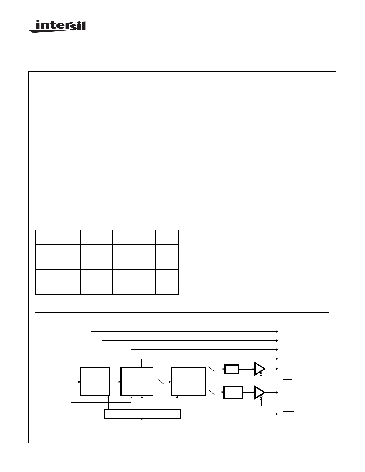
Address Sequencer
Description
The Intersil HSP45240 is a high speed Address Sequencer
which provides specialized addressing for functions like
FFTs, 1-D and 2-D filtering, matrix operations, and image
manipulation. The sequencer supports block oriented
addressing of large data sets up to 24-bits at clock speeds
up to 50MHz.
Specialized addressing requirements are met by using the
onboard 24 x 24 crosspoint switch. This feature allows the mapping of the 24 address bits at the output of the address generator to the 24 address outputs of the chip. As a result, bit rev erse
addressing, such as that used in FFTs, is made possible.
A single chip solution to read/write addressing is also made
possible by configuring the HSP45240 as two 12-bit
sequencers. To compensate for system pipeline delay, a programmable delay is provided on 12 of the address outputs.
The HSP45240 is manufactured using an advanced CMOS
process, and is a low power fully static design. The configuration of the device is controlled through a standard microprocessor interface and all inputs/outputs, with the e xception
of clock, are TTL compatible.9-
PKG.
NO.
Block Diagram
12
STARTIN
DLYBLK
CAUTION: These devices are sensitive to electrostatic discharge; follow proper IC Handling Procedures.
http://www.intersil.com or 407-727-9207
START
CIRCUITRY
SEQUENCE
GENERATOR
PROCESSOR INTERFACE
CS, A0, WR
D0-6,
| Copyright © Intersil Corporation 1999
24
CROSSPOINT
SWITCH
9-1
12
REG
DELAY
1-8
STARTOUT
ADDVAL
DONE
BLOCKDONE
OUT12-23
OEH
OUT0-11
OEL
BUSY
File Number 2489.3
Pinouts
HSP45240
ADDRESS SEQUENCER HSP45240
68 PIN PLASTIC LEADED CHIP CARRIER (PLCC)
GND
OUT23
OUT22
VCCOUT21
OUT20
GND
OUT19
OUT18
VCCOUT17
OUT16
GND
OUT15
9876543216867666564636261
NC
10
D0
11
D1
12
D2
13
D3
14
15
D4
16
D5
17
D6
18
GND
19
WR
20
A0
21
CS
22
GND
23
CLK
24
V
CC
25
RST
26
NC
OUT14
OUT13
4327 2829 30 31 32 33 34 35 36 37 38 39 40 41 42
NC
NC
60
OUT12
59
GND
58
OUT11
57
OUT10
56
V
55
CC
OUT9
54
OUT8
53
GND
52
OUT7
51
OUT6
50
V
49
CC
OUT5
48
OUT4
47
GND
46
OUT3
45
NC
44
NC
OEH
OEL
DLYBLK
STARTIN
STARTOUT
ADDVAL
CC
V
BUSY
GND
OUT0
DONE
BLOCKDONE
OUT1
CC
NC
V
OUT2
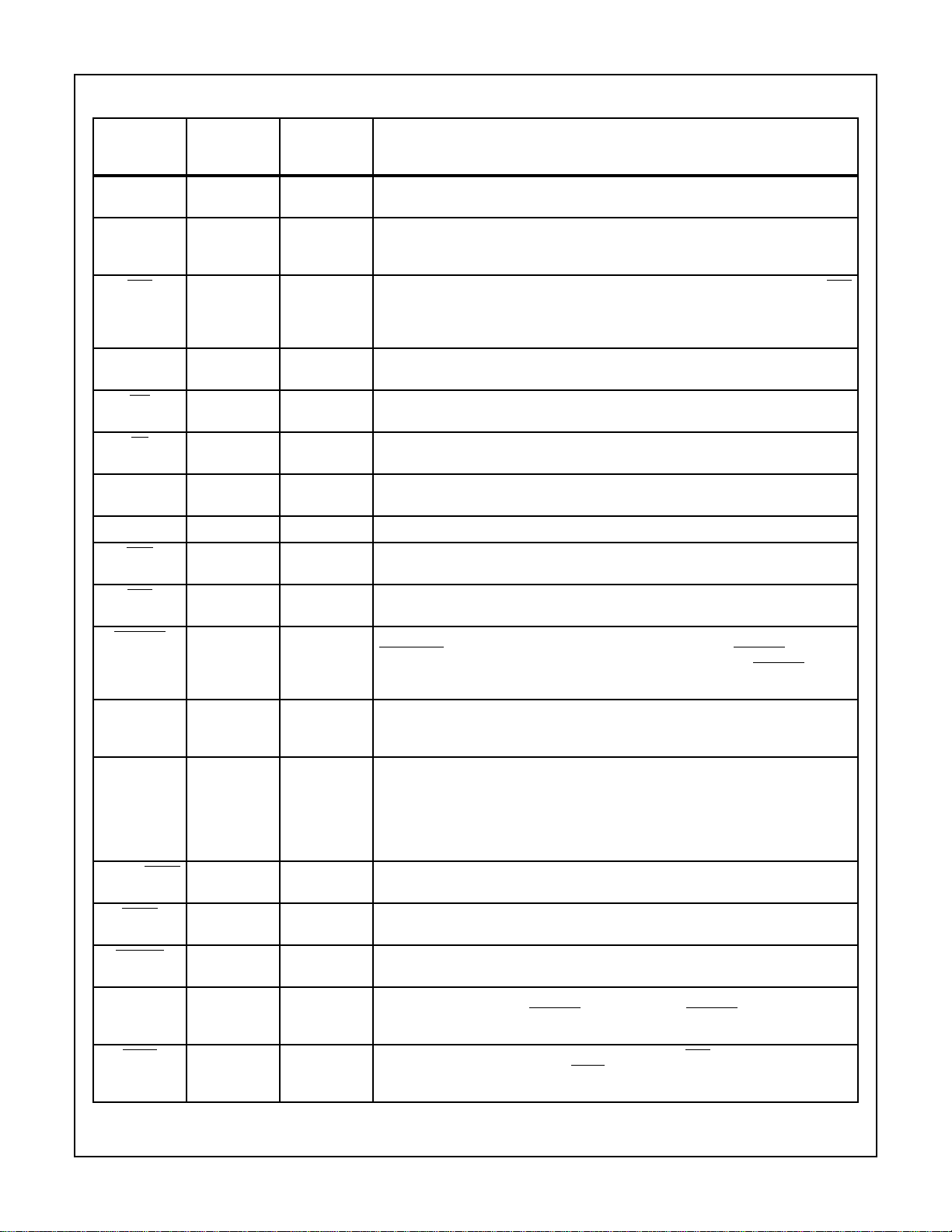
68 PIN GRID ARRAY (PGA)
BOTTOM VIEW
V
CC
ADD
VAL
BLOCK
DONE
BUSY
GND
DONE
OUT1
OUTO
OUT2
V
CC
NC
NC
GND
OUT5
OUT6
GND
OUT9
OUT10
OUT3
OUT4
V
CC
OUT7
OUT8
V
CC
OUT11
OEL
START
OUT
START
IN
L
K
J
H
G
F
E
D
NC
RST
CLK
CS
WR
D6
D4
OEH
NC
V
CC
GND
A0
GND
D5
D3
DLYBLK
OUT12
D2
C
B
A
D1
D0
NC
GND
2345678910111
OUT22
OUT23
OUT21
GND
OUT18
OUT17
OUT20
V
CC
OUT19
GND
OUT14
V
OUT16
CC
OUT15
GND
NC
OUT13
NC
9-2
Pin Descriptions
NAME TYPE
HSP45240
PLCC
PIN
NUMBER DESCRIPTION
V
CC
GND I 3, 9, 18, 22,
RST I 25 RESET: This active low input causes a chip reset which lasts for 26 clocks after RST
CLK I 23 CLOCK: The “CLK” signal is a CMOS input which provides the basic timing for address
WR I 19 WRITE: The rising edge of this input latches the data/address on D0-6 to be latched
CS I 21 CHIP SELECT: This active “low” input enables the configuration data/address on
A0 I 20 ADDRESS 0: This input defines D0-6 as a configuration register address if “high”, and
D0-6 I 11-17 DATA BUS: Data bus for Processor Interface.
OEH I 28 OUTPUT ENABLE HIGH: This asynchronous input is used to enable the output buffers
OEL I 29 OUTPUT ENABLE LOW: This asynchronous input is used to enable the output buffers
STARTIN I 31 START-IN: This active low input initiates an addressing sequence. May be tied to
DLYBLK I 30 DELA Y BLOCK: This activ e “high” input ma y be used to halt address gener ation on ad-
OUT0-23 O 39, 40, 42, 45,
BLOCK DONE O 36 BLOCK DONE: This active low output signals when the last address in an address block
DONE O 37 DONE: This active low output signals when the last address of an address sequence is
ADDVAL O 33 ADDRESS VALID: This active low output signals when the first address of an address
START-OUT O 32 ST ART-OUT: This active lo w output is generated when an address sequence is initiated
BUSY O 35 BUSY: This active low output is asserted one CLK after RST is deasserted and will re-
NOTE: #Denotes active low.
I 6, 24, 34, 41
49, 55, 68
38, 46, 52,
58, 65
47, 48, 50, 51,
53, 54, 56, 57,
59, 62-64, 66,
67, 1, 2, 4, 5,
7, 8
+5V power supply pin.
GROUND.
has been deasserted. The reset initializes the Crosspoint Switch and some of the configuration registers as described in the Processor Interface Section. The chip must be
clocked for reset to complete.
generation.
into the Processor Interface.
D0-6 to be latched into the Processor Interface.
configuration data if “low”, (see Processor Interface text).
for OUT 12-23.
for OUT0-11.
STARTOUT of another H5P45240 for multichip synchronization. STARTIN should only
be asserted for one CLK because address sequencing begins after STARTIN is deasserted.
dress block boundaries (see Sequence Generator text). The required timing relationship of this signal to the end of an address block is shown in Application Note 9205.
OUTPUT BUS: TTL compatible 24-bit Address Sequencer output.
is on OUT0-23.
on OUT0-23.
sequence is on 0UT0-23.
by a mechanism other thanSTARTIN. Ma y be tied to theSTAR TIN of other H5P45240’ s
for multichip synchronization.
main asserted for 25 CLK’s. While BUSY is asserted, all writes to the Processor Interface are disabled.
9-3
Functional Description
HSP45240
The Address Sequencer is a 24-bit programmable address
generator. As shown in the Block Diagram, the sequencer
consists of 4 functional blocks: the start circuitry, the
sequence generator, the crosspoint switch, and the processor interface. The addresses produced by the sequence
generator are input into the crosspoint switch. The crosspoint switch maps 24 bits of address input to a 24-bit output.
This allows for addressing schemes like “bit-reverse”
addressing for FFT’s. A programmable delay block is provided to allow the MSW of the output to be skewed from the
LSW . This feature may be used to compensate for processor
pipeline delay when the sequence generator is configured as
two independent 12-bit sequencers. Address Sequencer
operation is controlled by values loaded into configuration
registers associated with the sequence generator, crosspoint switch, and start circuitry. The configuration registers
are loaded through the processor interface.
Start Circuitry
The Start Circuitry generates the internal START signal
which causes the Sequence Generator to initiate an
addressing sequence. The START signal is produced by
writing the Processor Interface’s “Sequencer Start” address
(see Processor Interface text), by asserting the
input, or by the terminal address of a sequence generated
under “One-Shot Mode with Restart” (see Sequence Generator Section). Care should be taken to assert
only one clock cycle to ensure proper operation. A programmable delay from 1 to 31 clocks is provided to delay the initiation of an addressing sequence by delaying the internal
START signal (see Processor Interface text).
The Start Circuitry generates the output signal
which is asserted when the first valid output address is at the
pads. In addition, the Start Circuitry generates the
“
STARTOUT” signal for multichip synchronization. Note:
STARTOUT is only generated when an addressing
sequence is started by writing the “Sequencer Start”
address of the Processor Interface, or an internal START is
generated by reaching the end of an addressing sequence
produced by “One-Shot Mode with Restart”.
STARTlN
STARTlN for
ADDVAL
Sequence Generator
The Sequence Generator is a block oriented address generator. This means that the desired address sequence is subdivided into one or more address blocks, each containing a
user defined number of addresses. User supplied configuration data determines the number of address blocks and the
characteristics of the address sequence to be generated.
An address sequence is started when the control section of
the Sequence Generator receives the internal START signal
from the Start Circuitry. When the START signal is received,
the control section multiplexes the contents of the Start
Address Register and a “0” to the adder. The result of this
summation is the first address in the first block of the
address sequence. This value is stored in the Block Start
Address register by an enable generated from the control
section, and the multiplexers are switched to feed the output
of the Holding and Address Increment registers to the adder.
Address generation will continue with the Address Increment
added to the contents of the Holding Register until the first
address block has been completed.
An address block is completed when the number of
addresses generated since the beginning of the address
block equals the value stored in the Block Size register.
When the last address of the block is generated,
DONE is asserted to signal the end of the address block
(see Application Note 9205). On the following CLK, the multiplexers are configured to pass the contents of the Block
Start Address and Block Increment registers to the adder
which generates the first address of the next address block.
An enable from the control section allows this value to
update the Block Start Address register, and the multiplexers
are switched to feed the Holding and Address Increment registers to the adder for generation of the remaining addresses
in the block.
The address sequence is completed when the number of
address blocks generated equals the value loaded into the
Number of Blocks register. When the final address in the last
address block has been generated,
DONE are asserted to signal the completion of the address
sequence.
The parameters governing address generation are loaded
into five 24-bit configuration registers via the Processor
Interface. These parameters include the Start Address, the
beginning address of the sequence; the Block Size, the number of addresses in the address block; the Address Increment, the increment between addresses in a block; the
Number of Blocks, the number of address blocks in a
sequence (minimum 1); the Block Increment, the increment
between starting addresses of each block. The loading and
structure of these registers is detailed in the Processor Interface text.
DONE and BLOCK-
BLOCK-
As shown in Figure 1, the Sequence Generator is subdivided
into the address generation and control sections. The
address generation section performs an accumulation based
on the output of MUX1 and MUX2. The control section governs the operation of the multiplexers, enables loading of the
Block Start Address register, and signals completion of an
address sequence.
9-4
 Loading...