

Intersil Corporation HSP45116A Datasheet

HSP45116A
Data Sheet April 1999 File Number
Numerically Controlled Oscillator/
Modulator
The Intersil HSP45116A combines a high performance
quadrature numerically controlled oscillator (NCO) and a
high speed 16-bit Complex Multiplier/Accumulator (CMAC)
on a single IC. This combination of functions allows a
complex vector to be multiplied by the internally generated
(cos, sin) vector for quadrature modulation and
demodulation. As shown in the Block Diagram, the
HSP45116A is divided into three main sections. The Phase/
Frequency Control Section (PFCS) and the Sine/Cosine
Section together form a complexNCO. The CMAC multiplies
the output of the Sine/ Cosine Section with an external
complex vector.
The inputs to the Phase/Frequency Control Section consist
of a microprocessor interface and individual control lines.
The phase resolution of the PFCS is 32 bits, which results in
frequency resolution better than 0.013Hz at 52MHz. The
output of the PFCS is the argument of the sine and cosine.
The spurious free dynamic range of the complex sinusoid is
greater than 90dBc.
The output vector from the Sine/Cosine Section is one of the
inputs to the Complex Multiplier/Accumulator. The CMAC
multiplies this (cos, sin) vector by an external complex vector
and can accumulate the result. The resulting complex vectors
are available through two 20-bit output ports which maintain
the 90dB spectral purity. This result can be accumulated
internally to implement an accumulate and dump filter.
A quadrature down converter can be implemented by
loading a center frequency into the Phase/Frequency
Control Section. The signal to be down converted is the
Vector Input of the CMAC, which multiplies the data by the
rotating vector from the Sine/Cosine Section. The resulting
complex output is the down converted signal. The bit
position and widths for the outputs of CMAC and Complex
Accumulator (ACC) are programmable.
4156.3
Features
• NCO and CMAC on One Chip
• 52MHz Version
• 32-Bit Frequency Control
• 16-Bit Phase Modulation
• 16-Bit CMAC
• 0.013Hz Tuning Resolution at 52MHz
• Programmable Rounding Option
• Spurious Frequency Components < -90dBc
• Fully Static CMOS
Applications
• Frequency Synthesis
• Modulation - AM, FM, PSK, FSK, QAM
• Demodulation, PLL
• Phase Shifter
• Polar to Cartesian Conversions
Ordering Information
TEMP.
PART NUMBER
HSP45116AVC-52 0 to 70 160 Ld MQFP Q160.28x28
RANGE (oC) PACKAGE PKG. NO.
Block Diagram
MICROPROCESSOR
CONTROL SIGNALS
INTERFACE
INDIVIDUAL
3-197
VECTOR INPUT
RI
SINE/
PHASE/
FREQUENCY
CONTROL
SECTION
CAUTION: These devices are sensitive to electrostatic discharge; follow proper IC Handling Procedures.
COSINE
ARGUMENT
http://www.intersil.com or 407-727-9207
SINE/
COSINE
SECTION
SIN
COS
VECTOR OUTPUT
CMAC
RI
| Copyright © Intersil Corporation 1999

HSP45116A
Pinout
ENPHREG
ENOFREG
RBYTILD
BINFMT
PMSEL
IMIN0
RIN18
RIN17
RIN16
RIN15
RIN14
GND
RIN13
RIN12
RIN11
RIN10
RIN9
RIN8
RIN7
RIN6
RIN5
RIN4
RIN3
RIN2
GND
RIN1
V
CC
RIN0
SH1
SH0
ACC
PEAK
GND
TICO
V
CC
MOD1
MOD0
PACI
LOAD
NC
160 LEAD MQFP
TOP VIEW
CC
NC
V
159
160
1
2
3
4
5
6
7
8
9
10
11
12
13
14
15
16
17
18
19
20
21
22
23
24
25
26
27
28
29
30
31
32
33
34
35
36
37
38
39
40
41
42
IMIN3
IMIN2
GND
IMIN1
157
158
155
156
43444546474849505152535455565758596061626364656667686970717273747576777879
IMIN5
IMIN4
153
154
IMIN7
IMIN6
151
152
IMIN9
IMIN8
149
150
IMIN11
IMIN10
147
148
146
VCCIMIN12
145
GND
IMIN13
143
144
IMIN14
142
IMIN16
IMIN15
140
141
IMIN18
IMIN17
138
139
IO19
137
IO18
136
IO17
135
IO16
134
133
VCCIO15
132
GND
131
IO14
130
IO13
129
IO12
128
IO11
127
IO10
126
125
VCCGND
124
IO9
123
IO8
122
IO7
121
80
120
119
118
117
116
115
114
113
112
111
110
109
108
107
106
105
104
103
102
101
100
NC
GND
IO6
IO5
IO4
IO3
GND
IO2
IO1
V
CC
IO0
RO19
GND
RO18
RO17
RO16
RO15
RO14
V
CC
RO13
RO12
RO11
99
GND
98
RO10
97
RO9
96
V
95
CC
RO8
94
RO7
93
GND
92
RO6
91
RO5
90
RO4
89
RO3
88
V
87
CC
RO2
86
RO1
85
RO0
84
GND
83
DET1
82
DET0
81
CLROFR
ENCFREG
3-198
ENPHAC
ENTIREG
ENI
MODPI/2PI
CS
GND
CLK
C9
C8
CC
WR
C15
C14
C13
C12
C11
V
AD1
AD0
C10
C7C6C5C4C3C2C1
GND
C0
OUTMUX1
OUTMUX0
GND
OER
RND
OEREXT
OEI
OEIEXT
NC
PACO

HSP45116A
Pin Description
NAME NUMBER TYPE DESCRIPTION
V
CC
GND 7,20,32,48, 62,73,
C0-15 54-61, 63-70 I Control input bus for loading phase and frequency data into the PFCS. C15 is the MSB.
AD0-1 51, 52 I Address pins for selecting destination of C0-15 data. AD1 is the MSB.
CS 47 I Chip select (active low).
WR 53 I Write Enable. Data is clocked into the input register selected by AD0-1 on the rising edge of WR
CLK 49 I Clock. All registers, except the Control Registers clocked with WR, are clocked (when enabled)
ENPHREG 27 I Phase Register Enable (active low). Registered on chip by CLK. When active low, after being
ENOFREG 28 I Frequency Offset Register Enable (active low). Registered on chip by CLK. When active, after
ENCFREG 42 I Center Frequency Register Enable (active low). Registered on chip by CLK. When active, after
22, 34, 50, 87, 95,
102, 111, 124, 132,
145, 159
83, 92, 98, 108,
114, 119, 125, 131,
143, 157
- +5V Power supply input.
- Power supply ground input.
when the CS line is low.
by the rising edge of CLK.
clocked onto chip,ENPHREG enables the clocking of data into the Phase Register.
being clocked onto chip,ENOFREG enables clocking of frequency offset data into the frequency
offset register.
being clockedonto chip, ENCFREGenables clocking of datainto the Center FrequencyRegister.
ENPHAC 43 I Phase Accumulator Register Enable (active low). Registered on chip by CLK. When active, after
being clocked onto chip,ENPHAC enables clocking of the Phase Accumulator Register.
ENTIREG 44 I Time Interval ControlRegister Enable (activelow). Registered onchip by CLK. Whenactive, after
being clocked onto chip,ENTIREG enables clocking of data into the Time Accumulator Register.
ENI 45 I Real and Imaginary Data Input Register (RIR, IIR) Enable (active low). Registered on chip by
CLK. When active, after being clocked onto chip, ENI enables clocking of data into the real and
imaginary input data register.
MODPI/2PI 46 I Modulo π/2π Select. When low, the Sine and Cosine ROMs are addressed modulo 2π (360
degrees). When high, the mostsignificant address bitis held lowso that theROMs areaddressed
modulo π (180 degrees). This input is registered on chip by clock. This control pin was included
for FFT processing.
CLROFR 41 I Frequency Offset Register Output Zero (active low). Registered on chip by CLK. When active,
after being clocked onto chip, CLROFR zeros the data path from the Frequency Offset Register
to the frequency adder. New data can still be clocked into the Frequency Offset Register;
CLROFR does not affect the contents of the register.
LOAD 38 I Phase Accumulator Load Control (active low). Registered on chip byCLK. Zeroes feedback path
in the phase accumulator without clearing the Phase Accumulator Register.
MOD0-1 35, 36 I ExternalModulation Control Bits.When selectedwith the PMSELline, thesebits add a0, 90, 180,
or 270degree offsetto the currentphase inthe phase accumulator. Thelower 14bits of thephase
control path are set to zero.
These bits are loaded into the Phase Register when ENPHREG is low.
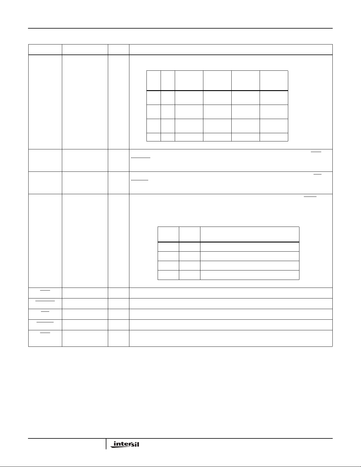
MOD1 MOD0 PHASE SHIFT (DEGREES)
00 0
01 90
1 0 270
1 1 180
3-199

HSP45116A
Pin Description
NAME NUMBER TYPE DESCRIPTION
PMSEL 39 I Phase Modulation Select Line. This line determines the source of the data clocked into the Phase
RBYTILD 30 I ROM Bypass, Timer Load (active low). Registered by CLK. This input bypasses the sine/ cosine
PACI 37 I Phase Accumulator Carry Input (active low). A low on this pin causes the phase accumulator to
PACO 79 O PhaseAccumulator Carry Output.Active lowand registeredby CLK.A lowon thisoutput indicates
TICO 33 O Time Interval Accumulator Carry Output. Active low, registered by CLK. This output goes low
RIN0-18 2-6, 8-19, 21, 23 I Real Input Data Bus. RIN18 is the MSB. This is the external real component into the complex
IMIN0-18 1, 138-142, 144,
(Continued)
146-156, 158
Register.When high, the Phase Control Registeris selected. When low ,the external modulation pins
(MOD0-1) are selected forthe most significant two bits and the least significant two bits and the least
significant 14 bits are set to zero. This control is registered by CLK.
ROM sothat the 16 bit phase adder output and lower16 bits of thephase accumulator go directly
to the CMAC’s sine and cosine inputs, respectively. It also enables loading of the Timer
Accumulator Register by zeroing the feedback in the accumulator.
increment by one in addition to the values in the Phase Accumulator Register and frequency
adder.
that the phase accumulator has overflowed, i.e., the end of one sine/cosine cycle has been
reached.
when a carry is generated by the time interval accumulator. This function is provided to time out
control events such as synchronizing register clocking to data timing.
multiplier.The busis clockedinto thereal Input DataRegister byCLK whenENI is asserted. Two’s
complement.
I Imaginary Input Data Bus. IMIN18 is the MSB. This is the external imaginary component into the
complex multiplier. The bus is clocked into the real Input Data Register by CLK when ENI is
asserted. Two’s complement.
SH0-1 24, 25 I Shift Control Inputs. Theselines control the input shifters of the RIN andIIN inputs of thecomplex
multiplier. The shift controls are common to the shifters on both of the busses.
SH1 SH0 SELECTED BITS
0 0 RIN0-15, IMIN0-15
0 1 RIN1-16, IMIN1-16
1 0 RIN2-17, IMIN2-17
1 1 RIN3-18, IMIN3-18
ACC 26 I Accumulate/Dump Control. This input controls the complex accumulators and their holding
registers. Whenhigh, the accumulators accumulateand the holding registers aredisabled. When
low, the feedback in the accumulators is zeroed to cause the accumulators to load.
The holding registers are enabled to clock in the results of the accumulation. This input is
registered by CLK.
BINFMT 31 I This input is used to convert the two’s complement output to offset binary (unsigned) for
applications using D/A converters. When low, bits RO19 and IO19 are inverted from the internal
two’s complement representation. This input is registered by CLK.
PEAK 29 I This input enables the peak detect feature of the block floating point detector. When high, the
maximum bit growth in the Output Holding Registers is encoded and output on the DET0-1 pins.
When the PEAK input is asserted, the block floating point detector output will track the maximum
growth in the holding registers, including the data in the Holding Registers at the time that PEAK
is activated.
3-200
HSP45116A
Pin Description
NAME NUMBER TYPE DESCRIPTION
OUTMUX0-1 71, 72 I These inputs select the data to be output on RO0-19 and IO0-19.
RO0-19 84-86, 88-91, 93,
IO0-19 110, 112, 113,
DET0-1 81, 82 O These output pins indicate the number of bits of growth in the accumulators. While PEAK is low,
(Continued)
94, 96, 97, 99-101,
103-107, 109
115-118, 121-123,
126-130, 133-137
OUT
OUT
MUX
MUX
1
0 RO16-19 RO0-15 IO16-19 IO0-15
0 0 Real CMAC
31-34
0 1 Real CMAC
31-34
1 0 Real ACC
16-19
1 1 Reserved Reserved Reserved Reserved
O Real Output Data Bus. R19 is the MSB. These three-state outputs are controlled by OER and
OEREXT. OUTMUX0-1 select the data output on the bus.
O ImaginaryOutput Data Bus. I19 is the MSB. These three-state outputs are controlled by OEI and
OEIEXT. OUTMUX0-1 select the data output on the bus.
these pins indicate the peak growth. The detector examines bits 15-18, real and imaginary
accumulator holding registers and bits30-33 of the real and imaginary CMAC Holding Registers.
The bits indicate the largest growth of the four registers.
Real CMAC
15-30
0, Real
CMAC 0-14
Real ACC
0-15
Imag CMAC
31-34
Imag CMAC
31-34
Imag ACC
16-19
Imag CMAC
15-30
0, Imag
CMAC 0-14
Imag ACC
0-15
NUMBER OF BITS
DET 1 DET 0
00 0
01 1
10 2
11 3
OER 74 I Three-state control for bits RO0-15. Outputs are enabled when the line is low.
OEREXT 76 I Three-state control for bits RO16-19. Outputs are enabled when the line is low.
OEI 78 I Three-state control for bits IO0-15. Outputs are enabled when the line is low.
OEIEXT 77 I Three-state control for bits IO16-19. Outputs are enabled when the line is low.
RND 75 I Round Enable. This input enables rounding of the output data precision from 9 to 20 bits. This
input is active “low”. This input must be tied either high or low.
OF GROWTH ABOVE 2
o
3-201

HSP45116A
Functional Description
The Numerically Controlled Oscillator/Modulator (NCOM)
produces a digital complex sinusoid waveform whose
amplitude, phase and frequency are controlled by a set of
input command words. When used as a Numerically
Controlled Oscillator (NCO), it generates 16-bit sine and
cosine vectors at a maximum sample rate of 40MHz. The
NCOM can be preprogrammed to produce a constant (CW)
sine and cosine output for Direct Digital Synthesis (DDS)
applications. Alternatively, the phase and frequency inputs
can be updated in real time to produce a FM, PSK, FSK, or
MSK modulated waveform. The Complex Multiplier/
Accumulator (CMAC) can be used to multiply this wa veform
by an input signal for AM and QAM signals. By stepping the
phase input, the output of the ROM becomes an FFT twiddle
factor; when data is input to the V ector Inputs (see Block
Diagram), the NCOM calculates an FFT butterfly.
As shown in the Block Diagram, the NCOM consists of
three parts: Phase and FrequencyControlSection (PFCS),
Sine/Cosine Generator, and CMAC. The PFCS stores the
phase and frequency inputs and uses them to calculate the
phase angle of a rotating complex vector. The Sine/Cosine
Generator performs a lookup on this phase and outputs the
appropriate values for the sine and cosine. The sine and
cosine form one set of inputs to the CMAC,whichmultiplies
them by the input vector to form the modulated output.
The outputs of the CMAC and ACC can be rounded to
different bit widths.
Phase and Frequency Control Section
The phase and frequency of the internally generated sine
and cosine arecontrolledby the PFCS (Figure 1). The PFCS
generates a 32-bit word that represents the current phase of
the sine and cosine waves being generated: The Sine/
Cosine Argument. Stepping this phase angle from 0 through
full scale (2
sinusoid starting at 0
counterclockwise. The PFCS automatically increments the
phase by a preprogrammed amount on every rising edge of
the external clock. The value of the phase step (which is the
sum of the Center and Offset Frequency Registers) is:
Phase Step =
where Signal Frequency is a 2’s complement number. The
sign bit will settheoutput vector notation for Upper Sideband
(USB) or lower Sideband (LSB) applications.
The PFCS is divided into two sections: The Phase
Accumulator uses the data on C0-15 to compute the phase
angle, that is the input to the Sine/Cosine Section (Sine/
Cosine Argument);theTime Accumulator supplies a pulseto
mark the passage of a preprogrammed period of time.
32
- 1) corresponds to the phase angle of a
o
and advancing around the unit circle
Signal Frequency
----------------------------------------------
Clock Frequency
232×
bit accumulator register every clock cycle; when the sum
causes the addertooverflow,the accumulation continues with
the 32 bits of the adder going into the Accumulator Register.
The overflow bit is used as an output to indicate the timing of
the accumulation overflows . In the Time Accum ulator, the
overflow bit generates
TICO, the Time Accumulator carry out
(which is the only output of the Time Accumulator). In the
Phase Accumulator, the overflow is inverted to generate the
Phase Accumulator Carry Out,
PACO.
The output of the Phase Accumulator goes to the Phase
Adder, which adds an offset to the top 16 bits of the phase.
This 32-bit number forms the argument of the sine and
cosine, which is passed to the Sine/Cosine Generator.
Both accumulators are loaded 16 bits at a time over the
C0-15 bus. Data on C0-15 is loaded into one of the three
input registers when
CS and WR are low. The data in the
Most Significant Input Register and Least Significant Input
Register forms a 32-bit word that is the input to the Center
Frequency Register, Offset Frequency Register and Time
Accumulator. These registers are loaded by enabling the
proper register enablesignal; for example,toloadthe Center
Frequency Register, the data is loaded into the LS and MS
Input Registers, and
edge of CLK will pass the registered version of
ENCFREG is set to zero; the nextrising
ENCFREG,
R.ENCFREG, to the clock enable of the Center Frequency
Register; this register then gets loaded on the following
rising edge of CLK. The contents of the Input Registers will
be continuously loaded into the Center Frequency Register
as long as
R.ENCFREG is low.
The Phase Register is loaded in a similar manner. Assuming
PMSEL is high, the contents of the Phase Input Register is
loaded into the Phase Register on every rising clock edge
that R.ENPHREG is low. If PMSEL is low, MOD0-1 supply
the two most significant bits into the Phase Register (MOD1
is the MSB) and the least significant 14 bits are loaded with
0. MOD0-1 and are used to generate a Quad Phase Shift
Keying (QPSK) signal (Table 2).
TABLE 1. AD0-1 DECODING
AD1 AD0
000
010
100
1 1 X X Reserved.
X X 1 X No Operation.
CS WR FUNCTION
Load leastsignificant bits
↑
of frequency input.
Load most significant bits
↑
of frequency input.
Load phase register.
↑
The Phase Accumulator and Time Accumulator work on the
same principle: a 32-bit word is added to the contents of a 32-
3-202
 Loading...