

Page 1

®
www.BDTIC.com/Intersil
HSP45102
Data Sheet April 25, 2007 FN2810.9
12-Bit Numerically Controlled Oscillator
The Intersil HSP45102 is Numerically Controlled Oscillator
(NCO12) with 32-bit frequency resolution and 12-bit output.
With over 69dB of spurious free dynamic range and worst
case frequency resolution of 0.009Hz, the NCO12 provides
significant accuracy for frequency synthesis solutions at a
competitive price.
The frequency to be generated is selected from two frequency
control words. A single control pin selects which word is used
to determine the output frequency. Switching from one
frequency to another occurs in one clock cycle, with a 6 clock
pipeline delay from the time that the new control word is
loaded until t4-he new frequency appears on the output.
Two pins, P0-1, are provided for phase modulation. They are
encoded and added to the top two bits of the phase
accumulator to offset the phase in 90° increments.
The 13-bit output of the Phase Offset Adder is mapped to the
sine wave amplitude via the Sine ROM. The output data
format is offset binary to simplify interfacing to D/A
converters. Spurious frequency components in the output
sinusoid are less than -69dBc.
The NCO12 has applications as a Direct Digital Synthesizer
and modulator in low cost digital radios, satellite terminals,
and function generators.
Features
• 33MHz, 40MHz Versions
• 32-Bit Frequency Control
• BFSK, QPSK Modulation
• Serial Frequency Load
• 12-Bit Sine Output
• Offset Binary Output Format
• 0.009Hz Tuning Resolution at 40MHz
• Spurious Frequency Components <-69dBc
• Fully Static CMOS
•Low Cost
• Pb-Free Plus Anneal Available (RoHS Compliant)
Applications
• Direct Digital Synthesis
• Modulation
• PSK Communications
• Related Products
- HI5731 12-Bit, 100MHz D/A Converter
Ordering Information
TEMP.
PART NUMBER PART MARKING
HSP45102SC-33 HSP45102SC-33 0 to +70 28 Ld SOIC (300 mil) M28.3
HSP45102SC-33Z (Note) HSP45102SC-33Z 0 to +70 28 Ld SOIC (300 mil) (Pb-free) M28.3
HSP45102SC-40 HSP45102SC -40 0 to +70 28 Ld SOIC (300 mil) M28.3
HSP45102SC-40Z (Note) HSP45102SC-40Z 0 to +70 28 Ld SOIC (300 mil)(Pb-free) M28.3
HSP45102SI-3396 HSP45102SI -33 0 to +70 28 Ld SOIC (300 mil) (Tape and Reel) M28.3
HSP45102SI-33Z (Note) HSP45102SI-33Z 0 to +70 28 Ld SOIC (300 mil) (Pb-free) M28.3
NOTE: Intersil Pb-free plus anneal products employ special Pb-free material sets; molding compounds/die attach materials and 100% matte tin plate
termination finish, which are RoHS compliant and compatible with both SnPb and Pb-free soldering operations. Intersil Pb-free products are MSL
classified at Pb-free peak reflow temperatures that meet or exceed the Pb-free requirements of IPC/JEDEC J STD-020.
RANGE (°C) PACKAGE
PKG.
DWG. #
1
CAUTION: These devices are sensitive to electrostatic discharge; follow proper IC Handling Procedures.
1-888-INTERSIL or 1-888-468-3774
| Intersil (and design) is a registered trademark of Intersil Americas Inc.
Copyright Intersil Americas Inc. 1999, 2004, 2005, 2007. All Rights Reserved
All other trademarks mentioned are the property of their respective owners.
Page 2
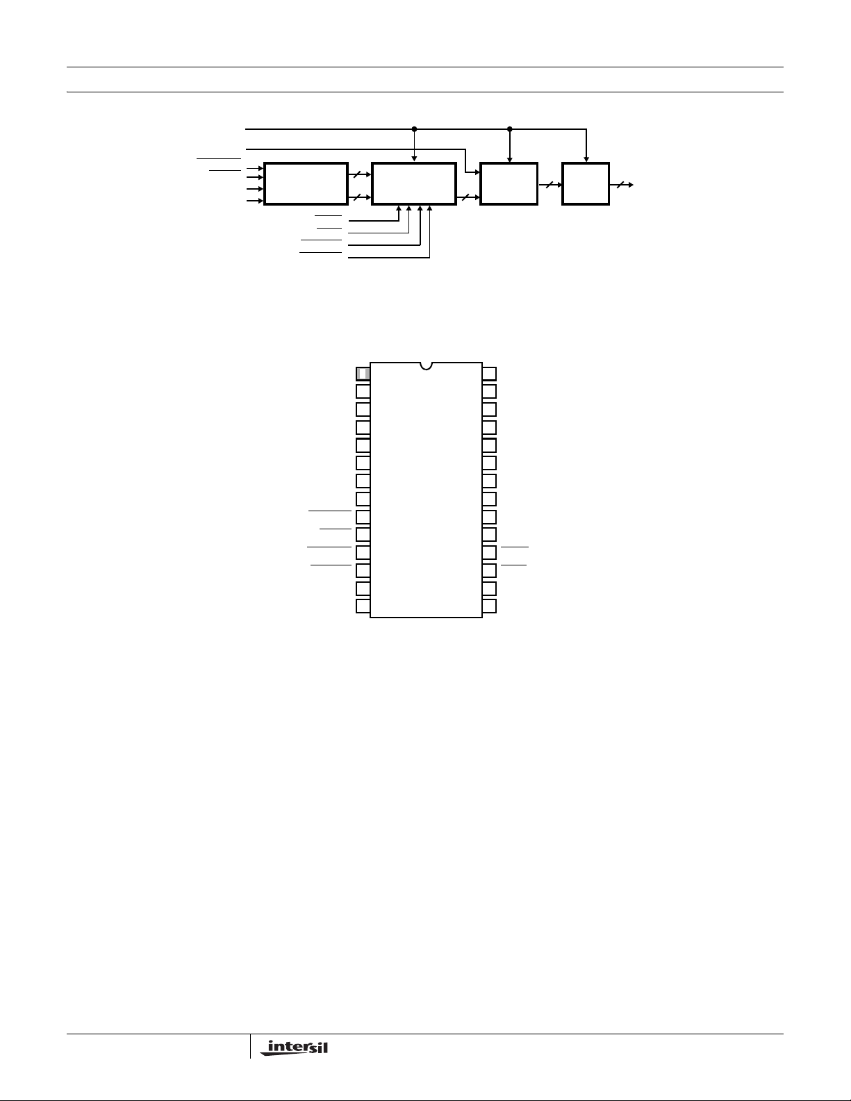
Block Diagram
www.BDTIC.com/Intersil
Pinout
CLK
PO-1
MSB/LSB
SFTEN
SD
SCLK
FREQUENCY
CONTROL
SECTION
LOAD
TXFR
ENPHAC
SEL_L/M
HSP45102
32
32
PHASE
ACCUMULATOR
HSP45102
(28 LEAD SOIC)
TOP VIEW
PHASE
OFFSET
13
ADDER
13 12
SINE
ROM
OUT0-11
OUT6
OUT7
OUT8
OUT9
OUT10
OUT11
GND
V
CC
SEL_L/ M
SFTEN
MSB/LSB
ENPHAC
SD
SCLK
OUT5
1
2
3
4
5
6
7
8
9
10
11
12
13
14
28
27
OUT4
26
OUT3
25
OUT2
24
OUT1
23
OUT0
22
V
CC
21
GND
20
P0
19
P1
18
LOAD
17
TXFR
16
CLK
15
GND
2
FN2810.9
April 25, 2007
Page 3
HSP45102
www.BDTIC.com/Intersil
Pin Description
NAME TYPE DESCRIPTION
V
CC
GND Ground
P0-1 I Phase modulation inputs (become active after a pipeline delay of four clocks). A phase shift of 0°, 90°,
CLK I NCO clock. (CMOS level)
SCLK I This pin clocks the frequency control shift register.
SEL_L/M
SFTEN
MSB/LSB
ENPHAC
SD I Data on this pin is shif te d int o th e fr equency regist er by the rising e dge of SCLK when SFTEN
TXFR
LOAD
OUT0-11 O Output data. OUT0 is LSB. Unsigned.
All inputs are TTL level, with the exception of CLK.
designates active low signals.
Overline
I A high on this input selects the least significant 32 bits of the 64-bit frequency register as the input to
I The active low input enables the shifting of the frequency register.
I This input selects the shift direction of the frequency register. A low on this input shifts in the data LSB
I This pin, when low, enables the clocking of the Phase Accumulator. This input has a pipeline delay of
I This active low input is clocked onto the chip by CLK and becomes active after a pipeline delay of four
I This input becomes active after a pipeline delay of five clocks. When low, the feedback in the phase
+5V power supply pin.
180°, or 270° can be selected as shown in Table 1.
the phase accumulator; a low selects the most significant 32 bits.
first; a high shifts in the data MSB first.
four clocks.
clocks. When low, the frequency control word selected by SEL_L/M
register to the phase accumulator’s input register.
accumulator is zeroed.
is transferred from the frequency
is low.
3
FN2810.9
April 25, 2007
Page 4

HSP45102
www.BDTIC.com/Intersil
PHASE OFFSET ADDER
P0-1
ENPHAC
TXFR
LOAD
CLK
SD
SCLK
SFTEN
MSB/LSB
SEL_L/M
4-DLY
R.P0-1
R.ENPHAC
R
R.TXFR
E
G
CLK
R.LOAD
R
E
G
FREQUENCY
CONTROL
SECTION
64-BIT
SHIFT
REG
32
/
32
/
FIGURE 1. NCO-12 FUNCTIONAL BLOCK DIAGRAM
Functional Description
The NCO12 produces a 12-bit sinusoid whose frequency
and phase are digitally controlled. The frequency of the sine
wave is determined by one of two 32-bit words. Selection of
the active word is made by SEL_L/M
output is controlled by the two-bit input P0-1, which is used
to select a phase offset of 0°, 90°, 180°, or 270°.
As shown in the Block Diagram, the NCO12 consists of a
Frequency Control Section, a Phase Accumulator, a Phase
Offset Adder and a Sine ROM. The Frequency Control
section serially loads the frequency control word into the
frequency register. The Phase Accumulator and Phase
Offset Adder compute the phase angle using the frequency
control word and the two phase modulation inputs. The Sine
ROM generates the sine of the computed phase angle. The
format of the 12-bit output is offset binary.
Frequency Control Section
The Frequency Control Section shown in Figure 1 serially
loads the frequency data into a 64-bit, bidirectional shift
register. The shift direction is selected with the MSB/LSB
input. When this input is high, the frequency control word on
the SD input is shifted into the register MSB first. When
MSB/LSB
is low the data is shifted in LSB first. The register
shifts on the rising edge of SCLK when SFTEN
timing of these signals is shown in Figures 2A and 2B.
The 64 bits of the frequency register are sent to the Phase
Accumulator Section where 32 bits are selected to control
the frequency of the sinusoidal output.
Phase Accumulator Section
The phase accumulator and phase offset adder compute the
phase of the sine wave from the frequency control word and
. The phase of the
is low. The
A
R.P0-1
13 MSBs
/
FRCTRL
0-31
FRCTRL
32-63
(HIGH SELECTS FRCTRL0-31, LOW SELECTS FRCTRL32-63)
D
D
E
R
0 1
13
/
CLK
32
/
‘0’
32
/
R.LOAD
ACCUMULATOR
32
/
MUX
R.TXFR
CLK
R
13
E
/
G
0 1
INPUT
REGISTER
R
E
G
R
SINE
E
ROM
G
32
/
MUX
A
D
D
E
R
32
/
R.ENPHAC
CLK
PHASE ACCUMULATOR
2-DLY
12
/
CLK
32
/
R
E
G
the phase modulation bits P0-1. The architecture is shown in
Figure 1. The most significant 13 bits of the 32-bit phase
accumulator are summed with the two-bit phase offset to
generate the 13-bit phase input to the Sine Rom. A value of
0 corresponds to 0°, a value of 1000 hexadecimal
corresponds to a value of 180°.
The phase accumulator advances the phase by the amount
programmed into the frequency control register. The output
frequency is equal to:
f
Nf
LO
N INT
× 232⁄(), or=
CLK
f
⎛⎞
⎜⎟
⎝⎠
OUT
-------------
f
CLK
32
2
,=
where N is the 32 bits of frequency control word that is
programmed. INT[•] is the integer of the computation. For
example, if the control word is 20000000 hexadecimal and the
clock frequency is 30MHz, then the output frequency would
be f
/8, or 3.75MHz.
CLK
The frequency control multiplexer selects the least
significant 32 bits from the 64-bit frequency control register
when SEL_L/M
when SEL_L/M
desired, SEL_L/M
is high, and the most significant 32 bits
is low. When only one frequency word is
and MSB/LSB must be either both high or
both low. This is due to the fact that when a frequency
control word is loaded into the shift register LSB first, it
enters through the most significant bit of the register. After
32 bits have been shifted in, they will reside in the 32 most
significant bits of the 64-bit register.
When TXFR
is asserted, the 32 bits selected by the freque ncy
control multiplexer are clocked into the phase accumulator
OUT0-11
R
E
G
32
/
(EQ. 1)
(EQ. 2)
4
FN2810.9
April 25, 2007
Page 5

HSP45102
www.BDTIC.com/Intersil
input register. At each clock, the contents of this register are
summed with the current contents of the accumulator to step to
the new phase. The phase accumulator stepping may be
inhibited by holdi ng ENPHAC
high. The phase accumulator
may be loaded with the value in the input register by asserting
LOAD
, which zeroes the feedback to the phase accumulator.
The phase adder sums the encoded phase modulation bits
P0-1 and the output of the phase accumulator to offset the
phase by 0°, 90°, 180° or 270°. The two bits are encoded to
produce the phase mapping shown in Table 1. This phase
mapping is provided for direct connection to the in-phase
and quadrature data bits for QPSK modulation.
SCLK
SD
SFTEN
1
0
TABLE 1. PHASE MAPPING
P0-1 CODING
P1 P0 PHASE SHIFT (DEGREES)
00 0
01 90
1 0 270
1 1 180
ROM Section
The ROM section generates the 12-bit sine value from the
13-bit output of the phase adder. The output format is offset
binary and ranges from 001 to FFF hexadecimal, centered
around 800 hexadecimal.
2
61
63
62
MSB/LSB
SFTEN
MSB/LSB
SCLK
SD
CLK
LOAD
TXFR
ENPHAC
FIGURE 2A. FREQUENCY LOADING ENABLED BY SFTEN
2
1
0
FIGURE 2B. FREQUENCY LOADING CONTROLLED BY SCLK
1 34 6789101152
61
63
62
SEL_L/M
OUT0-11
FIGURE 3. I/O TIMING
5
NEW
DATA
FN2810.9
April 25, 2007
Page 6

HSP45102
www.BDTIC.com/Intersil
Absolute Maximum Ratings T
Supply Voltage. . . . . . . . . . . . . . . . . . . . . . . . . . . . . . . . . . . . . +6.0V
Input, Output or I/O Voltage Applied . . . . . GND -0.5V to V
ESD Classification . . . . . . . . . . . . . . . . . . . . . . . . . . . . . . . . . Class 1
Operating Conditions
Operating Voltage Range (Commercial, Industrial) . . +4.75V to +5.25V
Operating Temperature Range (Commercial) . . . . . . . 0°C to +70°C
Operating Temperature Range (Industrial) . . . . . . . .-40°C to +85°C
CAUTION: Stresses above those listed in “Absolute Maximum Ratings” may cause permanent damage to the device. This is a stress only rating and operation of the
device at these or any other conditions above those indicated in the operational sections of this specification is not implied.
NOTE:
1. θ
is measured with the component mounted on an evaluation PC board in free air.
JA
= +25°C Thermal Information
A
Thermal Resistance (Typical, Note 1) θ
SOIC Package . . . . . . . . . . . . . . . . . . . . . . . . . . . 70
Maximum Junction Temperature . . . . . . . . . . . . . . . . . . . . . . +150°C
Maximum Storage Temperature Range. . . . . . . . . .-65°C to +150°C
Pb-free reflow profile . . . . . . . . . . . . . . . . . . . . . . . . . .see link below
http://www.intersil.com/pbfree/Pb-FreeReflow.asp
CC
+0.5V
Die Characteristics
Backside Potential . . . . . . . . . . . . . . . . . . . . . . . . . . . . . . . . . . . V
(°C/W)
JA
CC
DC Electrical Specifications
PARAMETER SYMBOL TEST CONDITIONS MIN MAX UNITS
Logical One Input Voltage V
Logical Zero Input Voltage V
High Level Clock Input V
Low Level Clock Input V
Output HIGH Voltage V
Output LOW Voltage V
Input Leakage Current I
Standby Power Supply Current I
Operating Power Supply Current I
CCSB
CCOP
IHC
ILC
OH
VCC = 5.25V 2.0 - V
IH
VCC = 4.75V - 0.8 V
IL
VCC = 5.25V 3.0 - V
VCC = 4.75V - 0.8 V
IOH = -400μA, VCC = 4.75V 2.6 - V
IOL = +2.0mA, VCC = 4.75V - 0.4 V
OL
VIN = VCC or GND, VCC = 5.25V -10 10 μA
I
VIN = VCC or GND, VCC = 5.25V, Note 4 - 500 μA
f = 33MHz, VIN = VCC or GND
V
= 5.25V, Notes 2 and 4
CC
-99 mA
Capacitance T
Input Capacitance C
Output Capacitance C
NOTES:
2. Power supply current is proportional to operating frequency. Typical rating for I
3. Not tested, but characterized at initial design and at major process/design changes.
4. Output load per test load circuit with switch open and C
= +25°C, Note 3
A
PARAMETER SYMBOL TEST CONDITIONS MIN MAX UNITS
FREQ = 1MHz, VCC = Open. All
IN
measurements are referenced to device
O
ground
CCOP
= 40pF.
L
-10 pF
-10 pF
is 3mA/MHz.
6
FN2810.9
April 25, 2007
Page 7

HSP45102
www.BDTIC.com/Intersil
AC Electrical Specifications V
PARAMETER SYMBOL NOTES
Clock Period t
Clock High t
Clock Low t
SCLK High/Low t
Setup Time SD to SCLK Going High t
Hold Time SD from SCLK Going High t
Setup Time SFTEN, MSB/LSB to SCLK Going High t
Hold Time SFTEN
Setup Time SCLK High to CLK Going High t
Setup Time P0-1 to CLK Going High t
Hold Time P0-1 from CLK Going High t
Setup Time LOAD
to CLK Going High
Hold Time LOAD
from CLK Going High
CLK to Output Delay t
Output Rise, Fall Time t
NOTES:
5. AC testing is performed as follows: Input levels (CLK Input) 4.0V and 0V; Input levels (all other inputs) 0V and 3.0V; Timing reference levels
(CLK) 2.0V; All others 1.5V. Output load per test load circuit with switch closed and C
< 1.5V.
V
OL
6. If TXFR
7. Controlled via design or process parameters and not directly tested. Characterized upon initial design and after major process and/or design
changes.
, MSB/LSB from SCLK Going High t
, TXFR, ENPHAC, SEL_L/M
, TXFR, ENPHAC, SEL_L/ M
is active, care must be taken to not violate setup and hold times as data from the shift registers may not have settled before CLK occurs.
= 5.0V ±5%, TA = 0°C to +70°C, TA = -40°C to +85°C (Note 5)
CC
-33 (33MHz) -40 (40MHz)
CP
CH
CL
SW
DS
DH
MS
MH
SS
PS
PH
t
ES
t
EH
OH
RF
Note 6 16 - 15 - ns
Note 7 8 - 8 - ns
30 - 25 - ns
12 - 10 - ns
12 - 10 - ns
12 - 10 - ns
12 - 12 - ns
0-0- ns
15 - 12 - ns
0-0- ns
15 - 12 - ns
1-1- ns
15 - 13 - ns
1-1- ns
215213 ns
= 40pF . Output transition is measured at VOH > 1.5V and
L
UNITSMIN MAX MIN MAX
AC Test Load Circuit
NOTE: Test head capacitance.
DUT
SWITCH S1 OPEN FOR I
7
CCSB
C
(NOTE)
L
AND I
S
1
CCOP
OH
±
1.5V I
I
EQUIVALENT CIRCUIT
OL
FN2810.9
April 25, 2007
Page 8

Waveforms
www.BDTIC.com/Intersil
CLK
HSP45102
t
CP
t
CH
t
CL
P0-1
LOAD, TXFR,
ENPHAC, SEL_L/M
OUT0-11
SCLK
SD
MSB/LSB
SFTEN
t
PS
t
ES
t
SW
t
DS
t
MS
,
t
SS
t
DH
t
MH
t
PH
t
EH
t
OH
t
SW
t
RF
FIGURE 4.
8
FN2810.9
April 25, 2007
Page 9

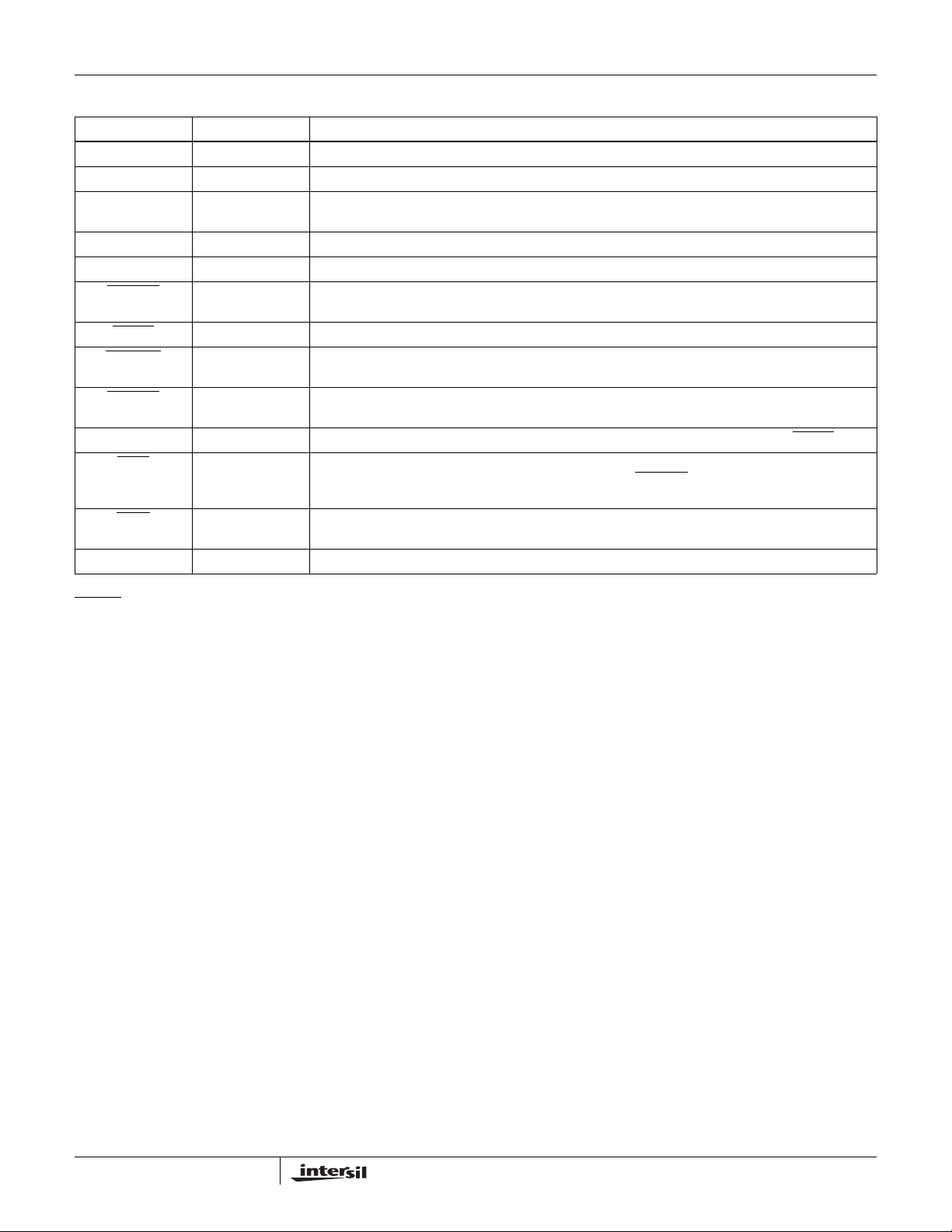
Small Outline Plastic Packages (SOIC)
www.BDTIC.com/Intersil
HSP45102
N
INDEX
AREA
123
-A-
E
-B-
SEATING PLANE
D
A
-C-
0.25(0.010) BM M
H
L
h x 45
o
α
e
B
0.25(0.010) C AM BS
NOTES:
1. Symbols are defined in the “MO Series Symbol List” in Section 2.2
of Publication Number 95.
2. Dimensioning and tolerancing per ANSI Y14.5M-1982.
3. Dimension “D” does not include mold flash, protrusions or gate
burrs. Mold flash, protrusion and gate burrs shall not exceed
0.15mm (0.006 inch) per side.
4. Dimension “E” does not include interlead flash or protrusions. Interlead flash and protrusions shall not exceed 0.25mm (0.010
inch) per side.
5. The chamfer on the body is optional. If it is not present, a visual
index feature must be located within the crosshatched area.
6. “L” is the length of terminal for soldering to a substrate.
7. “N” is the number of terminal positions.
8. Terminal numbers are shown for reference only.
9. The lead width “B”, as measured 0.36mm (0.014 inch) or greater
above the seating plane, shall not exceed a maximum value of
0.61mm (0.024 inch)
10. Controlling dimension: MILLIMETER. Converted inch dimensions are not necessarily exact.
M
A1
0.10(0.004)
M28.3 (JEDEC MS-013-AE ISSUE C)
28 LEAD WIDE BODY SMALL OUTLINE PLASTIC PACKAGE
INCHES MILLIMETERS
SYMBOL
A 0.0926 0.1043 2.35 2.65 -
A1 0.0040 0.0118 0.10 0.30 -
B 0.013 0.0200 0.33 0.51 9
C 0.0091 0.0125 0.23 0.32 -
D 0.6969 0.7125 17.70 18.10 3
E 0.2914 0.2992 7.40 7.60 4
e 0.05 BSC 1.27 BSC -
H 0.394 0.419 10.00 10.65 -
C
h 0.01 0.029 0.25 0.75 5
L 0.016 0.050 0.40 1.27 6
N28 287
o
α
0
o
8
o
0
o
8
Rev. 0 12/93
NOTESMIN MAX MIN MAX
-
All Intersil U.S. products are manufactured, assembled and tested utilizing ISO9000 quality systems.
Intersil Corporation’s quality certifications can be viewed at www.intersil.com/design/quality
Intersil products are sold by description only. Intersil Corporation reserves the right to make changes in circuit design, software and/or specifications at any time without
notice. Accordingly, the reader is cautioned to verify that data sheets are current before placing orders. Information furnished by Intersil is believed to be accurate and
reliable. However, no responsibility is assumed by Intersil or its subsidiaries for its use; nor for any infringements of patents or other rights of third parties which may result
from its use. No license is granted by implic atio n or other wise u nde r any p a tent or patent rights of Intersil or its subsidiaries.
For information regarding Intersil Corporation and its products, see www.intersil.com
9
FN2810.9
April 25, 2007
 Loading...