

Intersil Corporation HSP43881 Datasheet

HSP43881
Data Sheet May 1999
Digital Filter
The HSP43881 is a video speed Digital Filter (DF) designed
to efficiently implement vectoroperations such as FIR digital
filters. It is comprised of eight filter cells cascaded internally
and a shift and add output stage, all in a single integrated
circuit. Each filter cell contains a 8 x 8-bit multiplier, three
decimation registers and a 26-bit accumulator. The output
stage contains an additional 26-bit accumulator which can
add the contents of any filter cell accumulator to the output
stage accumulatorshifted right by 8 bits. The HSP43881 has
a maximum sample rate of 30MHz. The effective multiply
accumulate (mac) rate is 240MHz.
The HSP43881 DF can be configured to process expanded
coefficient and word sizes. Multiple DFs can be cascaded for
larger filter lengths without degrading the sample rate or a
single DF can process larger filter lengths at less than
30MHz with multiple passes. The architecture permits
processing filter lengths of over 1000 taps with the
guarantee of no overflows. In practice, most filter coefficients
are less than 1.0, making even larger filter lengths possible.
The DF provides for 8-bit unsigned or two’s complement
arithmetic, independently selectable for coefficients and
signal data.
Each DF filter cell contains three resampling or decimation
registers which permit output sample rate reduction at rates
1
of
/2, 1/3 or 1/4 the input sample rate. These registers also
provide the capability to perform 2-D operations such as
matrix multiplication and N x N spatial
correlations/convolutions for image processing applications.
File Number
2758.4
Features
• Eight Filter Cells
• 0MHz to 30MHz Sample Rate
• 8-Bit Coefficients and Signal Data
• 26-Bit Accumulator Per Stage
• Filter Lengths Over 1000 Taps
• Expandable Coefficient Size, Data Size and Filter Length
• Decimation by 2, 3 or 4
Applications
• 1-D and 2-D FIR Filters
• Radar/Sonar
• Adaptive Filters
• Echo Cancellation
• Complex Multiply-Add
• Sample Rate Converters
Ordering Information
PART
NUMBER
HSP43881JC-20 0 to 70 84 Ld PLCC N84.1.15
HSP43881JC-25 0 to 70 84 Ld PLCC N84.1.15
HSP43881JC-30 0 to 70 84 Ld PLCC N84.1.15
HSP43881GC-20 0 to 70 85 Ld PGA G85.A
HSP43881GC-25 0 to 70 85 Ld PGA G85.A
HSP43881GC-30 0 to 70 85 Ld PGA G85.A
TEMP. RANGE
(oC) PACKAGE PKG. NO.
Block Diagram
VCCV
DIENB
CIENB
DCMO - 1
ERASE
CIN0 - 7
RESET
ADR0 - 2
RESET
SHADD
SENBL
SENBH
TCCI
CLK
CLK
5
DF
FILTER
CELL 0
5
5
3
ADR0, ADR1, ADR2
2
SS
DIN0 - DIN7 TCS
8
8
88
26
2
8
DF
FILTER
CELL 1
8
26
1
8
DF
FILTER
CELL 2
8
26
SUM0 - 25
CAUTION: These devices are sensitive to electrostatic discharge; follow proper IC Handling Procedures.
8
DF
FILTER
CELL 3
OUTPUT
STAGE
8
26
MUX
26
26
8
DF
FILTER
CELL 4
http://www.intersil.com or 407-727-9207 | Copyright © Intersil Corporation 1999
8
26
8
DF
FILTER
CELL 5
8
26
8
DF
FILTER
CELL 6
8
26
8
DF
FILTER
CELL 7
26
8
TCCO
COUT0 - 7
COENB

Pinouts
HSP43881
85 PIN GRID ARRAY (PGA)
TOP VIEW, PINS DOWN
2173 4 5 6 8 9 10 11
V
A
B
C
D
E
F
G
H
J
K
COENB
V
SS
COUT7 ERASE DIN1 DIN2
V
CC
COUT5 COUT6
COUT3 COUT4
COUT1
V
COUT0 SHADD
SS
V
SS
ADR2 DCM0 CLK
ADR1
V
SUM25
CC
SENBH
SUM24
L
RESET
CC
DIN7
TCCO TCS
ALIGN
PIN
DIENB
COUT2
VCCSUM19
V
SS
DIN6 DIN3 DIN0 TCCI
CIENB
CIN7 CIN6 CIN4
DIN5 DIN4 CIN5 CIN3
CIN1
SUM0
SUM1
SUM16SUM17SUM20
SUM15 SUM12 SUM10 SUM8 SUM6
V
SS
SUM14SUM18SUM21SUM22SUM23DCM1
SUM13
V
CC
V
SS
HSP43881
TOP VIEW, PINS UP
1234567891011
V
V
CC
SS
V
CIN2
CIN0
SENBL
V
CCVSS
CC
SUM3 SUM2
SUM5 SUM4ADR0
V
SUM7
SS
SUM9SUM11
L
DCM1 SUM23 SUM22 SUM21 SUM18 SUM14 SUM13 SUM11 SUM9
K
SENBH SUM24 SUM19 SUM15 SUM12 SUM10 SUM8 SUM6
J
V
CC
H
ADR1
G
ADR2 DCM0 CLK
F
V
SS
E
COUT1
D
COUT3 COUT4
C
COUT5 COUT6
B
V
CC
A
V
SS
V
SSVCC
SUM25
ADR0
COUT0 SHADD
COUT2
V
SS
ALIGN
PIN
COENB V
CC
SUM20 SUM17 SUM16 SUM7
DIENB
ERASECOUT7 DIN8COUT8
RESET
V
CC
V
SS
DIN5 DIN4
DIN2DIN1
V
SUM1 SUM3 SUM2
SUM0
CIN1 CIN0
CIENB
DIN0DIN3DIN6DIN7
CIN8
SS
SUM5 SUM4
V
CIN2
CIN5 CIN3
V
V
CCVSS
SENBL
V
CIN4CIN6CIN7
CCVSS
SS
CC
2

HSP43881
Pinouts
(Continued)
SUM23
SUM22
V
CC
SUM21
SUM20
SUM19
SUM18
V
SS
SUM17
SUM16
V
CC
SUM15
SUM14
SUM13
SUM12
V
SS
SUM11
SUM10
SUM9
SUM8
SUM7
84 LEAD PLCC PACKAGE
BOTTOM VIEW
SS
SUM24
DCM1
V
111098765432184838281807978777675
12
13
14
15
16
17
18
19
20
21
22
23
24
25
26
27
28
29
30
31
32
33 34 35 36 37 38 39 40 41 42 43 44 45 46 47 48 49 50 51 52 53
SUM25
SENBH
CC
V
ADDR0
ADDR1
SS
DCM0
ADDR2
CLK
V
SHADD
COUT0
COUT1
SS
V
COUT2
COUT3
COUT4
COUT5
V
CC
COUT6
74
COUT7
73
72
V
SS
TCCO
71
COENB
70
V
69
68
67
66
65
64
63
62
61
60
59
58
57
56
55
54
CC
ERASE
RESET
DIENB
TCS
DIN7
DIN6
DIN5
DIN4
DIN3
DIN2
DIN1
DIN0
CIENB
TCCI
V
CC
SUM6
SS
V
SUM5
SUM4
CC
V
SUM3
SUM2
SUM1
SUM0
SS
V
NOTE: An overbar on a signal name represents an active LOW signal.
3
CIN0
SENBL
CIN1
CC
V
CIN2
CIN3
CIN4
CIN5
SS
V
CIN7
CIN6

HSP43881
Pin Description
PIN
SYMBOL
V
CC
V
SS
CLK G3 I The CLK input provides the DF system sample clock. The maximum clock frequency is 30MHz.
DIN0-7 A58, B67, C67 I These eight inputs are the data sample input bus. Eight bit data samples are synchronously loaded
TCS B5 I The TCS input determines the number system interpretation of the data input samples on pins
DIENB C5 I A low on this enables the data sample input bus (DIN0-7) to all the filter cells. A rising edge of the
CIN0-7 B9-11,
TCCI A9 I TheTCCI input determines the number system interpretation of the coefficient inputs on pins CIN07
CIENB B8 I A low on this input enable the C register of every filter cell and the D registers (decimation) of every
COUT0-7 B2, C1-2,
TCCO B3 O The TCCO three-state output determines the number system representation of the coefficients out-
COENB A2 I A low on the COENB input enables the COUT0-7 and the TCCO output. A high on this input places
NUMBER TYPE DESCRIPTION
A3, A10, B1,
D11, F10, J1,
K4, L7
A1, A11, E2,
F1, E11, H11,
K3, K6, L9
C10-11, D10,
E9-10
D1-2, E1, E3,
F2
+5V Power Supply Input.
Power Supply Ground Input.
through these pins to the X register of each filter cell simultaneously. The DIENB signal enables
loading, which is synchronous on the rising edge of the clock signal.
DIN0-7 as follows:
TCS = Low → Unsigned Arithmetic.
TCS = High → Two's Complement Arithmetic.
The TCS signal is synchronously loaded into the X register in the same way as the DIN0-7
inputs.
CLK signal occurring while DIENB is low will load the X register of every filter cell with the 8-bit value
present on DIN0-7. A high on this input forces all the bits of the data sample input bus to zero; a
rising CLK edge when DIENB is high will load the X register of every filter cell with all zeros. This
signal is latched inside the DF,delaying its effect by one clock internal to the DF. Therefore, it must
be low during the clock cycle immediately preceding presentation of the desired data on the
DIN0-7 inputs. Detailed operation is shown in later timing diagrams.
I These eight inputs are used to input the 8-bit coefficients. The coefficients are synchronously load-
ed into the C register of filter CELL 0 if a rising edge of CLK occurs while CIENB is low. The CIENB
signal is delayed by one clock as discussed below.
as follows:
TCCI = LOW E Unsigned Arithmetic.
TCCI = HIGH E Two's Complement Arithmetic.
The TCCI signal is synchronously loaded into the C register in the same way as the CIN0-7 inputs.
filter cell according to the state of the DCM0-1 inputs. A rising edge of the CLKsignaloccurring while
CIENB is low will load the C register and appropriate D registers with the coefficient data present at
their inputs. This provides the mechanism for shifting the coefficients from cell to cell through the
device. A high on this input freezes the contents of the C register and the D registers ignoring the
CLK signal. This signal is latched and delayed by one clock internal to the DF. Therefore, it must be
lowduring the clock cycle immediately preceding presentation of the desired coefficient of the CIN07 inputs. Detailed operation is shown in the Timing Diagrams Section.
O These eight three-state outputs are used to output the 8-bit coefficients from filter cell 7. These out-
puts are enabled by the COENB signal low. These outputs may be tied to the CIN0-7 inputs of the
same DF to recirculate the coefficients, or they may be tied to the CIN0-7 inputs of another DF to
cascade DFs for longer filter lengths.
put on COUTO-7. It tracks the TCCI signal to this same DF. It should be tied to the TCCI input of the
next DF in a cascade of DFs for increased filter lengths. This signal is enabled by COENB low.
all these outputs in their high impedance state.
4

HSP43881
Pin Description
SYMBOL
DCM0-1 G2, L1 These two inputs determine the use of the internal decimation registers as follows:
SUM0-25 J2, J5-8, J10,
SENBH K1 I A low on this input enables result bits SUM16-25. A high on this input places these bits in their high
SENBL E11 I A low on this input enables result bits SUM0-15. A high on this input places these bits in their high
ADR0-2 G1, H1-2 I These inputs select the one cell whose accumulator will be read through the output bus (SUM0-25)
SHADD F3 I The SHADD input controls the activation of the shift-and-add operation in the output stage. This
RESET A4 I A low on this input synchronously clears all the internal registers, except the cell accumulators. It
ERASE B4 I A low on this input synchronously clears the cell accumulator selected by the ADR0-1 signals. If
ALIGN PIN C3 Used for aligning chip in socket or printed circuit board. Must be left as a no connect in circuit.
(Continued)
PIN
NUMBER TYPE DESCRIPTION
DCM1 DCM0 Decimation Function
0 0 Decimation Registers not used.
0 1 One Decimation Register is used.
1 0 Two Decimation Registers are used.
1 1 Three Decimation Registers are used.
The coefficients pass from cell to cell at a rate determined by the number of decimation registers
used. When no decimation registers are used, coefficients move from cell to cell on each clock.
When one decimation register is used, coefficients move from cell to cell on every other clock, etc.
These signals are latched and delayed by one clock internal to the DF.
O These 26 three-state outputs are used to output the results of the internal filter cell computations.
K2, K5-11,
L-26, L8,
L10-11
Individual filter cell results or the result of the shift and add output stage can be output. If an individual filter cell result is to be output, the ADR0-2 signals select the filter cell result. The SHADD signal
determines whether the selected filter cell result or the output stage adder result is output. The signalsSENBHand SENBL enablethemostsignificantandleastsignificantbitsof the SUM0-25 result,
respectively. Both SENBH and SENBL may be enabled simultaneously if the system has a 26-bit or
larger bus. However, individual enables are provided to facilitate use with a 16-bit bus.
impedance state.
impedance state.
or added to the output stage accumulator. They also determine which accumulator will be cleared
when ERASE is low. For selection of which accumulator to read through the output bus (SUM0-25)
or which to add to the output stage accumulator, these inputs are latched in the DF and delayed by
one clock internal to the device. If the ADR0-2 lines remain at the same address for more than one
clock, the output at SUM0-25 will not change to reflect any subsequent accumulator updates in the
addressed cell. Only the result available during the first clock, when ADR0-1 selects the cell, will be
output. This does not hinder normal operation since the ADR0-1 lines are changed sequentially.
This feature facilitates the interface with slow memories where the output is required to be fixed for
more than one clock.
signal is latched in the DF and delayed by one clock internal to the device. A detailed explanation is
given in the DF Output Stage Section.
can be used with ERASE to also clear all the accumulators simultaneously.This signal is latched in
the DF and delayed by one clock internal to the DF.
RESET is also low simultaneously, all cell accumulators are cleared.
Functional Description
The Digital Filter Processor (DF) is composed of eight filter cells
cascaded together and an output stage for combining or
selectingfilte5r cell outputs(See Block Diagram). Each filter cell
contains a multiplier accumulator and sever al registers (Figure
1). Each 8-bit coefficient is multiplied by an 8-bit data sample,
with the result added to the 26-bit accumulator contents. The
coefficient output of each cell is cascaded to the coefficient
input of the next cell to its right.
DF Filter Cell
An 8-bit coefficient (CIN0-7) enters each cell through the C
register on the left and exits the cell on the right as signals
5
COUT0-7. With no decimation, the coefficient moves directly
from the C register to the output, and is valid on the clock
following its entrance. When decimation is selected the
coefficient exit is delayed by 1, 2 or 3 clocks by passing through
one or more decimation registers (D1, D2 or D3).
The combination of D registers through which the coefficient
passes is determined by the state of DCM0 and DCM1. The
output signals (COUT0-7) are connected to the CIN0-7 inputs
of the next cell to its right. The COENB input signal enables the
COUT0-7 outputs of the right most cell to the COUT-07 pins of
the device.
The C and D registers are enabled for loading by CIENB .
Loading is synchronous with CLK when CIENB is low.Note that
HSP43881
CIENB is latched internally. It enab les the register for loading
after the next CLK follo wing the onset of CIENB low. Actual
loading occurs on the second CLK following the onset of
CIENB low . Theref ore , CIENB must be lo w during the clock
cycle immediately preceding presentation of the coefficient on
the CIN0-7 inputs. In most basic FIR operations, CIENB will be
low throughout the process, so this latching and delay
sequence is only important during the initialization phase.
When CIENB is high, the coefficients are frozen.
These registers are cleared synchronously under control of
RESET, which is latched and delayed exactly like CIENB . The
output of the C register (C0-8) is one input to 8 x 8 multiplier.
The other input to the 8 x 8 multiplier comes from the output of
the X register. This register is loaded with a data sample from
the device input signals DIN0-7 discussed above . The X
register is enabled for loading by DIENB . Loading is
synchronous with CLK when DIENB is low.Note that DIENB is
latched internally . It enables the register for loading after the
next CLK follo wing the onset of DIENB low. Actual loading
occurs on the second CLK following the onset of DIENB low;
therefore, DIENB must be low during the clock cycle
immediately preceding presentation of the data sample on the
DIN0-7 inputs. In most basic FIR operations, DIENB will be low
throughout the process, so this latching and delay sequence is
only important during the initialization phase. When DIENB is
high, the X register is loaded with all zeros.
The multiplier is pipelined and is modeled as a multiplier core
followedby two pipeline registers,MREG0 and MREG1 (Figure
1). The multiplier output is sign extended and input as one
operand of the 26-bit adder. The other adder operand is the
output of the 26-bit accumulator. The adder output is loaded
synchronously into both the accumulator and the TREG.
The TREG loading is disabled by the cell select signal,
CELLn, where n is the cell number. The cell select is decoded
from the ADR0-2 signals to generate the TREG load enable.
The cell select is inverted and applied as the load enable to
the TREG. Operation is such that the TREG is loaded
whenever the cell is not selected. Theref ore, TREG is loaded
every clock except the clock following cell selection. The
purpose of the TREG is to hold the result of a sum of products
calculation during the clock when the accumulator is cleared
to prepare for the next sum of products calculation. This
allows continuous accumulation without wasting clocks .
decoded from ADR0-2 and the
ERASE signal enable clearing
of the accumulator on the next CLK.
The
ERASE and RESET signals clear the DF internal
registers and states as follows:
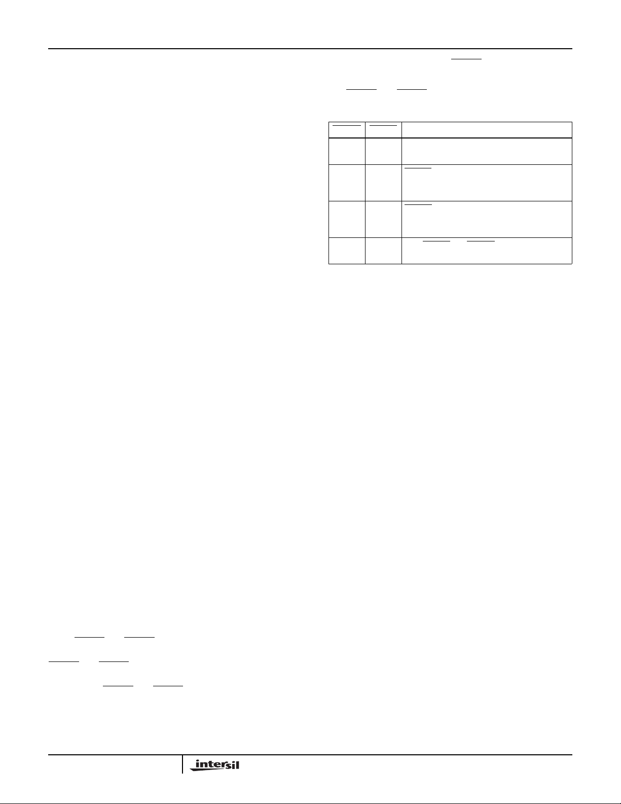
ERASE RESET CLEARING EFFECT
1 1 No clearing occurs, internal state remains
same.
10RESET only active, all registers except accu-
mulators are cleared, including the internal
pipeline registers.
01ERASE only active, the accumulator whose
address is given by the ADR0-2 inputs is
cleared.
0 0 BothRESETandERASE active, all accumula-
tors, as well as all other registers are cleared.
The DF Output Stage
The output stage consists of a 26-bit adder, 26-bit register,
feedback multiplexer from the register to the adder, an output
multiplexer and a 26-bit three-state driv er stage (Figure 2).
The 26-bit output adder can add any filter cell accumulator
result to the 18 most significant bits of the output buffer. This
result is stored back in the output buffer. This operation takes
place in one clock period. The eight LSBs of the output buffer
are lost. The filter cell accumulator is selected by the ADR0-2
inputs.
The 18 MSBs of the output buffer actually pass through the
zero mux on their wayto the output adder input. The zero mux
is controlled by the SHADD input signal and selects either the
output buffer 18 MSBs or all zeros for the adder input. A low
on the SHADD input selects zero. A high on the SHADD input
selects the output buffer MSBs, thus , activating the shift and
add operation. The SHADD signal is latched and delayed b y
one clock internally.
The accumulator is loaded with the adder output every clock
unless it is cleared. It is cleared synchronously in two ways.
When
RESET and ERASE are both low, the accum ulator is
cleared along with all other registers on the device. Since
ERASE and RESET are latched and delayed one clock
internally , clearing occurs on the second CLK f ollo wing the
onset of both
ERASE and RESET low.
The second accumulator clearing mechanism clears a single
accumulator in a selected cell. The cell select signal, CELLn,
6

DCM1.D
DCM0.D
RESET.D
CIENB.D
TCCI
CIN0-7
HSP43881
THREE-STATE BUFFERS
1
MUX
ON CELL 7 ONLY
TCCO
LD CLR
C REG
7
C.TCCI
0-7
C0-7
LD CLR
D1 REG
1
MUX
LD CLR
D2 REG
LD CLR
D3 REG
RESET.D
DIENB.D
TCS
DIN0-7
DCM1
DCM0
RESET
DIENB
CIENB
ADR0
ADR1
ADR2
ERASE
CLK
B
LD CLR
X REG
7
CLK
LATCHES
DCM1.D
DCM0.D
RESET.D
DIENB.D
CIENB.D
ADR0.D
ADR1.D
ADR2.D
ERASE.D
CLK
0
C0-8
X0-8
RESET.D
ACC.D0-25
D.TCCI
D0-7
CLK
MULTIPLIER
X
CORE
P0-17
MREG0
CLR
MREG1
CLR
0
C
0-17 SIGN EXTENSION
COUT0-7
COENB
CLK
18-25
CLK
ADR0
ADR1
ADR2
DECODER
ADDER
ACC0-25
CELL 0
CELL 1
CELL 7
ERASE.D
CELLn
CELLn
CLK
D Q
ACC
CLR
T REG
LD
AOUT0-25
CLK
FIGURE 1. FILTER CELL
7
 Loading...