


HSP43220
Data Sheet February 1999 File Number
Decimating Digital Filter
The HSP43220 Decimating Digital Filter is a linear phase
low pass decimation filter which is optimized for filtering
narrow band signals in a broad spectrum of a signal
processing applications. The HSP43220 offers a single chip
solution to signal processing applications which have
historically required several boards of ICs. This reduction in
component count results in faster development times as well
as reduction of hardware costs.
The HSP43220 is implemented as a two stage filter
structure. As seen in the block diagram, the first stage is a
high order decimation filter (HDF) which utilizes an efficient
sample rate reduction technique to obtain decimation up to
1024 through a coarse low-pass filtering process. The HDF
provides up to 96dB aliasing rejection in the signal pass
band. The second stage consists of a finite impulse
response (FIR) decimation filter structured as a transversal
FIR filterwithupto 512 symmetric taps which can implement
filters with sharp transition regions. The FIR can perform
further decimation by up to 16 if required while preserving
the 96dB aliasing attenuation obtained by the HDF. The
combined total decimation capability is 16,384.
2486.7
Features
• Single Chip Narrow Band Filter with up to 96dB
Attenuation
• DC to 33MHz Clock Rate
• 16-Bit 2’s Complement Input
• 20-Bit Coefficients in FIR
• 24-Bit Extended Precision Output
• Programmable Decimation up to a Maximum of 16,384
• Standard 16-Bit Microprocessor Interface
• Filter Design Software Available DECIMATE™
• Up to 512 Taps
Applications
• Very Narrow Band Filters
• Zoom Spectral Analysis
• Channelized Receivers
• Large Sample Rate Converter
The HSP43220 accepts 16-bit parallel data in 2’s
complement format at sampling rates up to 33 MSPS. It
provides a 16-bit microprocessor compatible interface to
simplify the task of programming and three-state outputs to
allow the connection of several ICs to a common bus. The
HSP43220 also provides the capability to bypass either the
HDF or the FIR for additional flexibility.
Block Diagram
DECIMATION UP TO 1024 DECIMATION UP TO 16
INPUT CLOCK
DATA INPUT
CONTROL AND COEFFICIENTS
16
16
HIGH ORDER
DECIMATION
FILTER
Ordering Information
TEMP.
PART NUMBER
HSP43220VC-33 0 to 70 100 Ld MQFP Q100.14x20
HSP43220JC-15 0 to 70 84 Ld PLCC N84.1.15
HSP43220JC-25 0 to 0 84 Ld PLCC N84.1.15
HSP43220JC-33 0 to 70 84 Ld PLCC N84.1.15
HSP43220GC-25 0 to 70 84 Ld CPGA G84.A
HSP43220GC-33 0 to 70 84 Ld CPGA G84.A
DECIMATE Software Development Tool (This software tool may be
downloaded from our Internet site: http://www.intersil.com)
DECIMATION
FIR CLOCK
RANGE (oC) PACKAGE PKG. NO.
FIR
FILTER
24
DATA OUT
DATA READY
3-194
CAUTION: These devices are sensitive to electrostatic discharge; follow proper IC Handling Procedures.
http://www.intersil.com or 407-727-9207
DECIMATE™ is a trademark of Intersil Corporation.
| Copyright © Intersil Corporation 1999
HSP43220
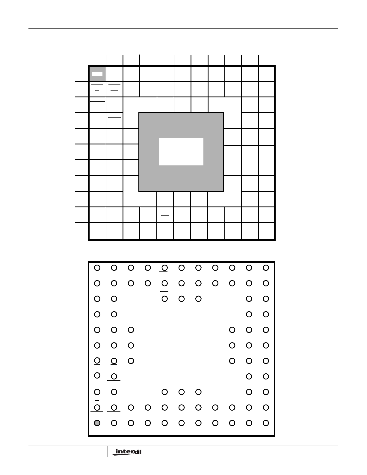
Pinouts
84 PIN GRID ARRAY (PGA)
1 23456789 1110
_
A
B
C
D
E
GND
STAR T
IN
ASTAR T
IN
A1
CS WR
DATA
IN 1
STAR T
OUT
V
CC
RESET
_
_
DATA
IN 2
DATA
IN 0
A0
DATA
IN 4
_
DATA
IN 3
_
_
DAT A
DATA
IN 7
IN 8
_
_
DAT A
DATA
IN 6
IN 13
_
DAT A
DATA
IN 5
IN 9
_
DATA
DATA
IN 11
IN 14
_
_
DATA
DATA
IN 12
IN 15
_
_
DATA
IN 10
HSP43220
C_BUS15C_BUS
C_BUS
F
10
C_BUS
C_BUS
G
12
C_BUS
H
9
J
K
L
C_BUS
GND
C_BUS
C_BUS
8
C_BUS6C_BUS3C_BUS2C_BUS
14
C_BUS
13
11
V
CC
7
C_BUS
4
5
C_BUS
1
0
TOP VIEW
PINS DOWN
OUT_
GND
SELH
_
OUT
V
ENP
OUT
ENX
CC
_
DATA
RDY
_
FIR
CK
DATA
GND
OUT 22
_
DATA
V
CC
OUT 23
_
_
_
_
V
CC
CK_IN
DATA
OUT 5
DATA
OUT 9
DATA
OUT 10
DATA
OUT 19
DATA
OUT 21
GND GND
V
DATA
OUT 0
DATA
OUT 3
_
DATA
OUT 6
_
V
_
GND
DATA
OUT 13
DATA
OUT 16
_
DATA
OUT 17
_
DATA
OUT 20
CC
CC
_
_
_
_
_
_
_
DATA_
OUT 1
DATA
OUT 2
DATA
OUT 4
DATA
OUT 7
DATA
OUT 8
DATA
OUT 11
DATA_
OUT 12
DATA
OUT 14
DATA
OUT 15
DATA
OUT 18
_
_
_
_
_
_
_
_
12 3456789 11
L
C_BUS6C_BUS3C_BUS2C_BUS
K
J
H
G
F
E
D
C
B
A
C_BUS
8
GND
C_BUS
9
C_BUS
12
C_BUS
10
CS WR
A1
ASTAR T
IN
START
IN
GND
C_BUS
C_BUS
C_BUS
V
C_BUS
11
C_BUS15C_BUS
RESET
V
START
OUT
DATA
IN 1
CC
CC
4
5
7
C_BUS
13
14
A0
DATA
IN 0
_
DATA
IN 2
_
_
0
C_BUS
1
DATA
IN 3
DATA
IN 4
OUT
ENX
OUT
ENP
OUT_
SELH
HSP43220
BOTTOM VIEW
DATA
IN 5
_
DATA
IN 6
_
DATA
IN 7
_
DATA
RDY
_
V
CC
GND
PINS UP
_
DATA
IN 9
_
DATA
IN 13
_
DATA
IN 8
_
V
CC
GND
_
FIR
CK
_
DATA
IN 10
_
DATA
IN 12
_
DATA
IN 11
_
_
_
DATA
OUT 23
DATA
OUT 22
DATA
IN 15
DATA
IN 14
_
_
_
_
DATA
OUT 21
DATA
OUT 19
DATA
OUT 10
DATA
OUT 9
DATA
OUT 5
CK_IN
V
_
_
_
_
_
CC
10
DATA
OUT 20
DATA
OUT 17
DATA
OUT 16
DATA
OUT 13
GND
V
CC
DATA
OUT 6
DATA
OUT 3
DATA
OUT 0
V
CC
GND GND
_
_
_
_
_
_
_
DATA
OUT 18
DATA
OUT 15
DATA
OUT 14
DATA_
OUT 12
DATA
OUT 11
DATA
OUT 8
DATA
OUT 7
DATA
OUT 4
DATA
OUT 2
DATA_
OUT 1
_
_
_
_
_
_
_
_
3-195
HSP43220
Pinouts
(Continued)
GND
GND
NC
STARTOUT
V
CC
V
CC
STARTIN
ASTARTIN
RESET
A1
A0
WR
CS
C_BUS15
C_BUS14
C_BUS13
C_BUS12
C_BUS11
C_BUS10
C_BUS9
V
CC
V
CC
GND
GND
C_BUS8
C_BUS7
C_BUS6
NC
C_BUS5
C_BUS4
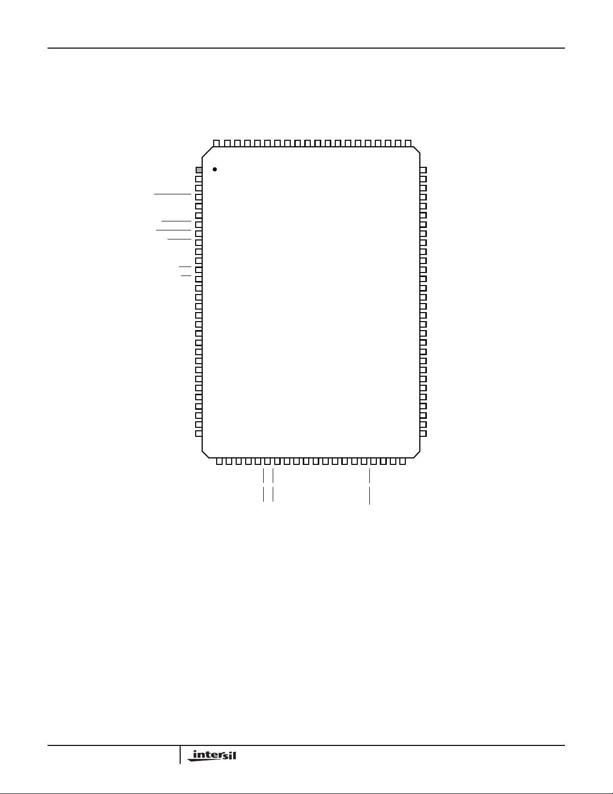
100 LEAD MQFP
TOP VIEW
VCCGND
GND
VCCDATA_IN15
DATA_IN14
DATA_IN13
DATA_IN12
DATA_IN11
DATA_IN10
DATA_IN9
DATA_IN8
DATA_IN7
DATA_IN6
DATA_IN5
DATA_IN0
DATA_IN1
99 98 97 96 95 94 93 91 89 87 85 84 83 818286889092100
1
2
3
4
5
6
7
8
9
10
11
12
13
14
15
16
17
18
19
20
21
22
23
24
25
26
27
28
29
30
DATA_IN3
DATA_IN2
DATA_IN4
80
79
78
77
76
75
74
73
72
71
70
69
68
67
66
65
64
63
62
61
60
59
58
57
56
55
54
53
52
51
CK_IN
V
CC
V
CC
GND
GND
DATA_OUT0
DATA_OUT1
DATA_OUT2
DATA_OUT3
DATA_OUT4
DATA_OUT5
DATA_OUT6
DATA_OUT7
DATA_OUT8
DATA_OUT9
DATA_OUT10
DATA_OUT11
GND
GND
V
CC
V
CC
DATA_OUT12
DATA_OUT13
DATA_OUT14
DATA_OUT15
DOUT_OUT16
DATA_OUT17
DATA_OUT18
DATA_OUT19
DATA_OUT20
32 33 34 35 36 37 38 40 42 44 46 47 48 50494543413931
C_BUS3
C_BUS2
C_BUS1
C_BUS0
V
OUT_ENP
OUT_ENX
OUT_SELH
CC
CC
V
GND
GND
CC
V
FIR_CK
CC
V
GND
GND
DATA_RDY
DATA_OUT21
DATA_OUT23
DATA_OUT22
3-196

HSP43220
Pinouts
(Continued)
84 PLASTIC LEADED CHIP CARRIER (PLCC)
VCCGND
CK_IN
DATA_OUT 21
DATA_OUT 20
DATA_OUT 19
CC
V
74
73
72
71
70
69
68
67
66
65
64
63
62
61
60
59
58
57
56
55
54
DATA_OUT 18
GND
DATA_OUT 0
DATA_OUT 1
DATA_OUT 2
DATA_OUT 3
DATA_OUT 4
DATA_OUT 5
DATA_OUT 6
DATA_OUT 7
DATA_OUT 8
DATA_OUT 9
DATA_OUT 10
DATA_OUT 11
GND
V
CC
DATA_OUT 12
DATA_OUT 13
DATA_OUT 14
DATA_OUT 15
DATA_OUT 16
DATA_OUT 17
STARTOUT
V
STARTIN
ASTARTIN
RESET
WR
C_BUS 15
C_BUS 14
C_BUS 13
C_BUS 12
C_BUS 11
C_BUS 10
C_BUS 9
V
GND
C_BUS 8
C_BUS 7
C_BUS 6
CC
A1
A0
CS
CC
DATA_IN 1
DATA_IN 0
GND
DATA_IN 2
DATA_IN 3
DATA_IN 4
DATA_IN 5
DATA_IN 6
DATA_IN 7
DATA_IN 8
DATA_IN 9
DATA_IN 10
DATA_IN 11
DATA_IN 12
DATA_IN 13
DATA_IN 14
DATA_IN 15
111098765432184838281807978777675
12
13
14
15
16
17
18
19
20
21
22
23
24
25
26
27
28
29
30
31
32
33 34 35 36 37 38 39 40 41 42 43 44 45 46 47 48 49 50 51 52 53
CC
CC
V
V
GND
GND
C_BUS 5
C_BUS 4
C_BUS 3
C_BUS 2
C_BUS 1
C_BUS 0
OUT_ENP
OUT_SELH
OUT_ENX
FIR_CK
DATA_RDY
DATA_OUT 23
DATA_OUT 22
Pin Description
NAME TYPE DESCRIPTION
V
CC
GND The device ground.
CK_IN I Input Sample Clock. Operations in the HDF are synchronous with the rising edge of this clock signal. The maximum clock
FIR_CK I Input Clock for the FIR Filter. This clock must be synchronous with CK_IN. Operations in the FIR are synchronous with the
DATA_IN0-15 I Input Data Bus. This bus is used to provide the 16-bit input data to the HSP43220. The data must be provided in a synchro-
C_BUS0-15 I Control Input Bus. This input bus is used to load all the filter parameters. The pins WR, CS and A0, A1 are used to select
DATA_OUT
0-23
DATA_RDY O An active high output strobe that is synchronous with FIR_CK that indicates that the result of the just completed FIR cycle
RESET I RESET is an asynchronous signal which requires that the input clocks CK_IN and FIR_CK are active when RESET is as-
WR I Write Strobe. WR is used for loading the internal registers of the HSP43220. When CS and WR are asserted, the rising edge of
CS I Chip Select. The Chip Select input enables loading of the internal registers. When CS and WR are low,the A0 and A1 address
The +5V power supply pins.
frequency is 33MHz. CK_IN is synchronous with FIR_CK and thus the two clocks maybe tied together if required, or CK_IN
can be divided down from FIR_CK. CK_IN is a CMOS level signal.
rising edge of this clock signal. The maximum clock frequency is 33MHz. FIR_CK is a CMOS level signal.
nous fashion, and is latched on the rising edge of the CK_IN signal. The data bus is in 2's complement fractional format. Bit
15 is the MSB.
the destination of the data on the Control bus and write the Control bus data into the appropriate register as selected by A0
and A1
O Output Data Bus. This 24-Bit output port is used to provide the filtered result in 2's complement format. The upper 8 bits of
the output, DATA_OUT16-23 will provide extension or growth bits depending on the state of OUT_SELH and whether the
FIR has been put in bypass mode. Output bits DATA_OUT0-15 will provide bits 20 through 2-15 when the FIR is not bypassed and will provide the bits 2-16 through 2-31 when the FIR is in bypass mode.
is available on the data bus.
serted. RESET disables the clock divider and clears all of the internal data registers in the HDF. The FIR filter data path is
not initialized. The control register bits that are cleared are F_BYP, H_STAGES,and H_DRATE. The F_DIS bit is set. In order
to guarantee consistent operation of the part, the user must reset the DDF after power up.
WR will latch the C_BUS0-15 data into the register specified by A0 and A1.
lines are decoded to determine the destination of the data on C_BUS0-15. The rising edge of WR then loads the appropriate
register as specified by A0 and A1.
3-197

HSP43220
Pin Description
NAME TYPE DESCRIPTION
A0, A1 I Control Register Address. These lines are decoded to determine which control register is the destination for the data on
ASTARTIN I ASTARTIN is an asynchronous signal which is sampled on the rising edge of CK_IN. It is used to put the DDF in operational
STARTOUT O STARTOUT is a pulse generated from the internally synchronized version of ASTARTIN. It is provided as an output for use
STARTIN I STARTIN is a Synchronous Input. A high to low transition of this signal is required to start the part. STARTIN is sampled on
OUT_SELH I Output Select. The OUT_SELH input controls which bits are provided at output pins DATA_OUT16-23. A HIGH on this control
OUT_ENP I Output Enable. The OUT_ENP input controls the state of the lower 16 bits of the output data bus, DATA_OUT0-15. A LOW on
OUT_ENX I Output Enable. The OUT_ENX input controls the state of the upper 8 bits of the output data bus, DATA_OUT16-23. A LOW
The HDF
The first filter section is called the High Order Decimation Filter
(HDF) and is optimized to perform decimation by large factors .
It implements a low pass filter using only adders and delay
elements instead of a large number of multiplier/ accumulators
that would be required using a standard FIR filter.
The HDF is divided into 4 sections: the HDF filter section,
the clock divider, the control register logic and the start logic
(Figure 1).
Data Shifter
After being latched into the Input Register the data enters the
Data Shifter. The data is positioned at the output of the shifter
(Continued)
C_BUS0-15. Register loading is controlled by the A0 and A1, WR and CS inputs.
mode. ASTARTIN is internally synchronized to CK_IN and is used to generateSTARTOUT.
in multi-chip configurations to synchronously start multiple HSP43220's. The width of STARTOUT is equal to the period of
CK_IN.
the rising edge of CK_IN. This synchronous signal can be used to start single or multiple HSP43220's.
line selects bits 28 through 21 from the accumulator output. A LOW on this control line selects bits 2-16 through 2-23 from
the accumulator output. Processing is not interrupted by this pin.
this control line enables the lower 16 bits of the output bus. When OUT_ENP is HIGH, the output drivers are in the high impedance state. Processing is not interrupted by this pin.
on this control line enables the upper 8 bits of the output bus. When OUT_ENX is HIGH, the output drivers are in the high
impedance state. Processing is not interrupted by this pin.
Integrator Section
The data from the shifter goes to the Integrator section.
This is a cascade of 5 integrator (or accumulator) stages,
which implement a low pass filter. Each accumulator is
implemented as an adder followed by a register in the feed
forward path. The integrator is clocked by the sample clock,
CK_IN as shown in Figure 2. The bit width of each integrator
stage goes from 66 bits at the first integrator down to 26 bits
at the output of the fifth integrator.Bit truncation is performed
at each integrator stage because the data in the integrator
stages is being accumulated and thus is growing, therefore
the lower bits become insignificant, and can be truncated
without losing significant data.
to preventerrors due to overflowoccurring at the output of the
HDF. The number of bits to shift is controlled by H_GROWTH.
A0-1 WR CS C_BUS
H_GROWTH INT_EN1-5
DAT A
IN
CK_IN
CK_DEC
CK_IN
H_DRATE
CONTROL
REGISTER LOGIC
655
COMB_EN1-5
H_BYP
CLOCK
DIVIDER
CK DEC
HDF FILTER SECTION
ISTART COMB_EN1-5H_GROWTH INT_EN1-5 RESETRESET
INPUT
REG
6
DAT A
SHIFTER
FIGURE 1. HIGH ORDER DECIMATION FILTER FIGURE
5
INTEGRATOR
DEC
REG
26661616
3-198
RESET
26
RESET ASTAR TINCK_IN
ISTART
5
COMB FILTER ROUND REG
START
LOGIC
19
16
STARTIN
STARTOUT
TO FIR
16
TO FIR
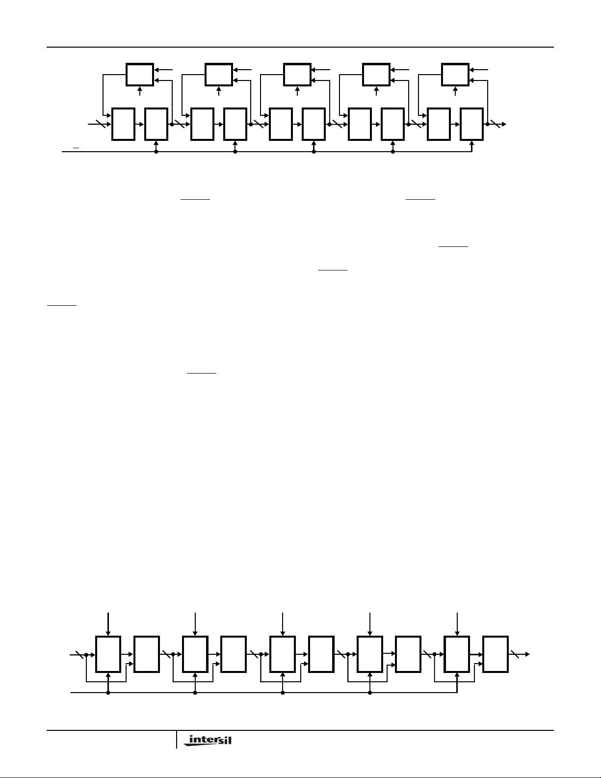
HSP43220
FROM
SHIFTER
CK IN
0
MUX
INT_EN5
66 63
REG
INT_EN4
MUX
0
REG
53
FIGURE 2. INTEGRATOR
There are three signals that control the integrator section;
they are H_STAGES, H_BYP and
RESET. In Figure 2 these
control signals have been decoded and are labelled
INT_EN1 - INT_EN5. The order of the filter is loaded via the
control bus and is called H_STAGES. H_STAGES is
decoded to provide the enables for each integrator stage.
When a given integrator stage is selected, the feedback path
is enabled and the integrator accumulates the current data
sample with the previous sum. The integrator section can be
put in bypass mode by the H_BYP bit. When H_BYP or
RESET is asserted, the feedback paths in all integrator
stages are cleared.
Decimation Register
The output of the Integrator section is latched into the
Decimation Register by CK_DEC. The output of the
Decimation register is cleared when
RESET is asserted. The
HDF decimation rate = H_DRATE +1, which is defined as
H
for convenience.
DEC
Comb Filter Section
The output of the Decimation Register is passed to the
Comb Filter Section. The Comb section consists of 5
cascaded Comb filters or differentiators. Each Comb filter
section calculates the difference between the current and
previous integrator output. Each Comb filter consists of a
register which is clocked by CK_DEC, followed by an
subtractor, where the subtractor calculates the difference
between the input and output of the register. Bit truncations
are done at each stage as shown in Figure 3. The first
stage bit width is 26 bits and the output of the fifth stage is
19 bits.
MUX
INT_EN3
REG
0
MUX
INT_EN2
43
REG
0
MUX
INT_EN1
∑∑∑∑∑
35
REG
0
TO
DECIMATION
REGISTER
26
There are three signals that control the Comb Filter; H_
STAGES, H_BYP and
RESET. In Figure 3 these control
signals are decoded as COMB_EN1 - COMB_EN5. The
order of the Comb filter is controlled by H_STAGES, which is
programmed over the control bus. H_BYP is used to put the
comb section in bypass mode.
RESET causes the register
output in each Comb stage to be cleared. The H_ BYP and
RESET control pins, when asserted force the output of all
registers to zero so data is passed through the subtractor
unaltered. When the H_STAGES control bits enable a given
stage the output of the register is subtracted from the input.
It is important to note that the Comb filter section has a speed
limitation. The Input sampling rate divided by the decimation
factor in the HDF (CK_IN/H
) should not exceed 4MHz.
DEC
Violating this condition causes the output of the filter to be
incorrect. When the HDF is put in bypass mode this limitation
does not apply .Equation1 describes the relationship between
F_TAPS, F_DRA TE, H_DRATE, CK_IN and FIR_CK.
Rounder
The filter accuracy is limited by the 16-bit data input. To
maintain the maximum accuracy, the output of the comb is
rounded to 16 bits.
The Rounder performs a symmetric round of the 19-bit
output of the last Comb stage. Symmetric rounding is done
to prevent the synthesis of a 0Hz spectral component by the
rounding process and thus causing a reduction in spurious
free dynamic range. Saturation logic is also provided to
prevent roll over from the largest positive value to the most
negative value after rounding. The output of the last comb
filter stage in the HDF section has a 16-bit integer portion
with a 3-bit fractional part in 2's complement format.
FROM
DECIMATION
REGISTER
26
CK_DEC
COMB_EN5
RESET
REG
BAA-B
3-199
22
COMB_EN4
RESET
REG
COMB_EN3
RESET
BAA-B
REG
21
FIGURE 3. COMB FILTER
COMB_EN2
RESET
BAA-B
19
REG
20
BAA-B
19
COMB_EN1
RESET
REG
TO
ROUNDER
BAA-B

HSP43220
The rounding algorithm is as follows:
POSITIVE NUMBERS
Fractional Portion Greater Than or Equal to 0.5 Round Up
Fractional Portion Less Than 0.5 Truncate
NEGATIVE NUMBERS
Fractional Portion Less Than or Equal to 0.5 Round Up
Fractional Portion Greater Than 0.5 Truncate
The output of the rounder is latched into the HDF output
register with CK_DEC. CK_DEC is generated by the Clock
Divider section. The output of the register is cleared when
RESET is asserted.
Clock Divider and Control Logic
The clock divider divides CK_IN by the decimation factor
H
to produce CK_DEC. CK_DEC clocks the Decimation
DEC
Register, Comb Filter section, HDF output register. In the
FIR filter CK_DEC is used to indicate that a new data
sample is available for processing. The clock generator is
cleared by
started by an internal start signal (see Start Logic).
The Control Register Logic enables the updating of the Control
registers which contain all of the filter parameter data. When
WR and CS are asserted, the control register addressed by bits
A0 and A1 is loaded with the data on the C_BUS.
DDF Control Registers
F_Register (A1 = 0, A0 = 0)
F_OAD F_BYP F_ESYM F_DRATE F_TAPS
FA0 FB0 ES0 D3 D2 D1 D0 T8 T7 T6 T5 T4 T3 T2 T1 T0
15 14 13 1211109876543210
F_TAPS
Bits T0-T8 are used to specify the number of FIR filter taps. The number
entered is one less than the number of taps required. For example, to
specify a 511 tap filter F_TAPS would be programmed to 510. The minimum number of FIR taps = 3 (F_TAPS = 2).
F_DRATE
Bits D0-D3 are used to specify the amount of FIR decimation. The number entered is one less than the decimation required. For example, to
specify decimation of 16, F_DRATEwould be programmed to 15. For no
FIR decimation, F_DRATE would be set equal to 0. FDRATE +1 is
defined as F
F_ESYM
Bit ES0 is used to select the FIR symmetry.F_ESYM is set equal to one
to select even symmetry and set equal to zero to select odd symmetry.
When F_ESYM is one, data is added in the pre-adder; when it is zero,
data is subtracted. Normally set to one.
F_BYP
FB0 is used to select FIR bypass mode. FIR bypass mode is selected by
setting F_BYP = 1. When FIR bypass mode is selected, the FIR is internally set up for a 3 tap even symmetric filter, no decimation (F_DRATE =
0) and F_OAD is set equal to one to zero one side of the preadder. In FIR
bypass mode all FIR filter parameters, except F_CLA, are ignored, including the contents of the FIR coefficient RAM. In FIR bypass mode the output data is brought output on the lower 16 bits of the output bus
DATA_OUT 0-15. To disable FIR bypass mode, F_BYP is set equal to
zero. When F_BYP is returned to zero, the coefficients must be reloaded.
F_OAD
Bit FA0 is used to select the zero the preadder mode. This mode zeros
one of the inputs to the pre-adder. Zero preadder mode is selected by
setting F_OAD equal to one. This feature is useful when implementing
arbitrary phase filters or can be used to verify the filter coefficients. To
disable the Zero Preadder mode F_OAD is set equal to zero.
DEC
.
RESET and is not enabled until the DDF is
3-200
FIGURE 4.

HSP43220
DDF Control Registers
FC_Register (A1 = 0, A0 = 1)
C19 C18 C17 C16 C15 C14 C13 C12 C11 C10 C9 C8 C7 C6 C5 C4
XXXXXXXXXXXXC3C2C1C0
1514131211109876543210
(Continued)
F_CF
F_CF
Bits C0-C19 represent the coefficient data, where C19 is the MSB. Two writes are
required to write each coefficient which is 2's complement fractional format. The first
write loads C19 through C4; C3 through C0 are loaded on the second write cycle. As
the coefficients are written into this register they are formatted into a 20-bit coefficient
and written into the Coefficient RAM sequentially starting with address location zero.
The coefficients must be loaded sequentially, with the center tap being the last coefficient to be loaded. See coefficient RAM, below.
FIGURE 5.
H_Register 1 (A1 = 1, A0 = 0)
RESERVED F_DIS F_CLA H_BYP H_DRATE
FD0 FC0 HB0 R9 R8 R7 R6 R5 R4 R3 R2 R1 R0
151413 12 11 10 9876543210
H_DRATE Bits
R0-R9 are used to select the amount of decimation in the HDF. The amount of decimation selected is programmed as the required decimation minus one; for instance
to select decimation of 1024 H_DRATE is set equal to 1023. HDRATE +1 is defined
as H
DEC
.
H_BYP
Bit HB0 is used to select HDF bypass mode. This mode is selected by setting H_BYP =
1. When this mode is selected the input data passes through the HDF unfiltered. Internally H_ST A GES and H_DRATE are both set to zero and H_GROWTH is set to 50.
H_REGISTER 2 must be reloaded when H_BYP is returned to 0. To disable HDF
bypass mode H_BYP = 0. The relationship between CK_IN and FIR_CK in this and all
other modes is defined by Equation 1.
F_CLA
Bit FC0 is used to select the clear accumulator mode in the FIR. This mode is enabled
by setting F_CLA = 1 and is disabled by setting F_CLA = 0. In normal operation this bit
should be set equal to zero. This mode zeros the feedback path in the accumulator of
the multiplier/accumulator (MAC). It also allows the multiplier output to be clocked off
the chip by FIR_CK, thus DATA_RDY has no meaning in this mode. This mode can be
used in conjunction with the F_OAD bit to read out the FIR coefficients from the coefficient RAM.
F_DIS
Bit FD0 is used to select the FIR disable mode. This feature enables the FIR parameters to be changed. This feature is selected by setting F_DIS = 1. This mode terminates the current FIR cycle. While this feature is selected, the HDF continues to
process data and write it into the FIR data RAM. When the FIR re-programming is
completed, the FIR can be re-enabled either by clearing F_DIS, or by asserting one of
the start inputs, which automatically clears F_DIS.
3-201
FIGURE 6.

HSP43220
DDF Control Registers
H_Register 2 (A1 = 1, A0 = 1)
RESERVED H_GROWTH H_STAGES
15 14 13 12 11 10 9 8 7 6 5 4 3 2 1 0
(Continued)
G5 G4 G3 G2 G1 G0 N2 N1 N0
H_STAGES
Bits N0-N2 are used to select the number of stages or order of the
HDF filter. The number that is programmed in is equal to the
required number of stages. For a 5th order filter, H_STAGES
would be set equal to 5.
H_GROWTH
Bits G0-G5 are used to select the proper amount of growth bits.
H_GROWTH is calculated using the following equation:
H_GROWTH = 50 - CEILING {H_STAGES X log (H
where the CEILING { } means use the next largest integer of the
result of the value in brackets and log is the log to the base 10.
The value of H_GROWTH represents the position of the LSB on
the output of the data shifter.
FIGURE 7.
DEC
)/ log(2)}
Start Logic
The Start Logic generates a start signal that is used
internally to synchronously start the DDF. If
asserted (
STARTIN must be tied high) the Start Logic
synchronizes it to CK_IN by double latching the signal and
generating the signal
8. The
STARTOUT signal is then used to synchronously start
STARTOUT, which is shown in Figure
other DDFs in a multi-chip configuration (the
signal of the first DDF would be tied to the
second DDF). The NAND gate shown in Figure 8 then
passes this synchronized signal to be used on chip to
provide a synchronous start. Once started, the chip requires
a
RESET to halt operation.
RESET
ASTARTIN
CK_IN
When
STARTIN is asserted (ASTARTINmust be tied high) the
NAND gate passes
S
DQ
FIGURE 8. START LOGIC
STARTIN which is used to provide the
S
DQ
internal start, ISTART, for the DDF. When
the internal start signal is held inactive, thus it is necessary to
assert either
ASTARTIN or STARTIN in order to start the DDF.
The timing of the first validDATA_INwith respect to
is shown in the Timing Waveforms.
ASTARTIN is
STARTOUT
STARTIN of the
STARTIN
ISTART
STARTOUT
RESET is asserted
START_IN
In using
ASTARTIN or STARTIN a high to low transition must
be detected by the rising edge of CK_IN, therefore these
signals must have been high for more than one CK_IN cycle
and then taken low.
The FIR Section
The second filter in the top level block diagram is a Finite
Impulse Response (FIR) filter which performs the final
shaping of the signal spectrum and suppresses the aliasing
components in the transition band of the HDF. This enables
the DDF to implement filters with narrow pass bands and
sharp transition bands.
The FIR is implemented in a transversal structure using a
single multiplier/accumulator (MAC)and RAM for storage of the
data and filter coefficients as shown in Figure 9. The FIR can
implement up to 512 symmetric taps and decimation up to 16.
The FIR is divided into 2 sections: the FIR filter section and
the FIR control logic.
Coefficient RAM
The Coefficient RAM stores the coefficients for the current FIR
filter being implemented. The coefficients are loaded into the
Coefficient RAM over the control bus (C_BUS). The
coefficients are written into the Coefficient RAM sequentially ,
starting at location zero. It is only necessary to write one half
of the coefficients when symmetric filters are being
implemented, where the last coefficient to be written in is the
center tap.
3-202

HSP43220
The coefficients are loaded into address 01 in two writes.
The first write loads the upper 16 bits of the 20-bit
coefficient, C4 through C19. The second write loads the
lower 4 bits of the coefficient, C0 through C3, where C19 is
the MSB. The two 16-bit writes are then formatted into the
20-bit coefficient that is then loaded into the Coefficient RAM
starting at RAM address location zero, where the coefficient
at this location is the outer tap (or the first coefficient value).
To reload coefficients, the Coefficient RAM Address pointer
must be reset to location zero so that the coefficients will be
loaded in the order the FIR filter expects. There are two
methods that can be used to reset the Coefficient RAM
address pointer. The first is to assert
RESET, which
automatically resets the pointer, but also clears the HDF and
alters some of the control register bits. (
RESET does not
change any of the coefficient values.) The second method is
to set the F_DIS bit in control register H_ REGISTER1. This
control bit allows any of the FIR control register bits to be reprogrammed, but does not automatically modify any control
registers. When the programming is completed, the FIR is
re-started by clearing the F_DIS bit or by asserting one of
the start inputs (
ASTARTIN or STARTIN). The F_DIS bit
allows the filter parameters to be changed more quickly and
is thus the recommended reprogramming method.
section of the OPERATIONAL SECTION there is a chart that
shows the tradeoffs between these parameters.)
FIR_CK
CK_IN TAPS/2()4F
----------------------------------------------------------------------------------
≥
H
++[]
DEC
DECFDEC
(EQ. 1)
This equation expresses the minimum FIR_CK. The
minimum FIR_CK is the smallest integer multiple of CK_IN
that satisfies Equation 1. In addition, the TSK specification
must be met (see AC Electrical Specifications). F
decimation rate in the FIR (F
= F_DRATE +1), where
DEC
DEC
is the
TAPS = the number of taps in the FIR for even length filters
and equals the number of taps+1 for odd length filters.
Solving the above equation for the maxim um n umber of taps:
TAPS 2
=
FIR_CK H
--------------------------------------------------------- - F
DECFDEC
CK_IN
DEC
-4–
(EQ. 2)
In using this equation, it must be kept in mind that CK_IN/
H
must be less than or equal to 4MHz (unless the HDF
DEC
is in bypass mode in which case this limitation in the HDF
does not apply). In the OPERATIONAL SECTION under the
Design Considerations, there is a table that shows the tradeoffs of these parameters. In addition, Intersil provides a
software package called DECIMATE™ which designs the
DDF filter from System specifications.
Data RAM
The Data RAM stores the data needed for the filter
calculation. The format of the data is:
0.2-12-22-32-42-52-62-72-82-92-102-112-122-132-142-15
2
where the sign bit is in the 20 location.
The 16-bit output of the HDF Output Register is written into
the Data Ram on the rising edge of CK_DEC.
RESET initializes the write pointer to the data RAM. After a
RESET occurs, the output of the FIR will not be valid until
the number of new data samples written to the Data RAM
equals TAPS.
The filter always operates on the most current sample and
the taps-1 previous samples. Thus if the F_DIS bit is set,
data continues to be written into the data RAM coming from
the HDF section. When the FIR is enabled again the filter will
be operating on the most current data samples and thus
another transient response will not occur.
The maximum throughput of the FIR filter is limited by the
use of a single Multiplier/Accumulator (MAC). The data
output from the HDF being clocked into the FIR filter by
CK_DEC must not be at a rate that causes an erroneous
result being calculated because data is being overwritten.
The equation shown below describes the relationship
between, FIR_CK, CK_DEC, the number of taps that can be
implemented in the FIR, the decimation rate in the HDF and
the decimation rate in the FIR. (In the Design Considerations
The registered outputs of the data RAM are added or
subtracted in the 17-bit pre-adder. The F_OAD control bit
allows zeros to be input into one side of the pre-adder. This
provides the capability to implement non-symmetric filters.
The selection of adding the register outputs for an even
symmetric filter or for subtracting the register outputs for odd
symmetric filter is provided by the control bit F_ESYM, which
is programmed over the control bus. When subtraction is
selected, the new data is subtracted from the old data. The
17-bit output of the adder forms one input of the
multiplier/accumulator.
A control bit F_CLA provides the capability to clear the
feedback path in the accumulator such that multiplier output
will not be accumulated, but will instead flow directly to the
output register. The bit weightings of the data and
coefficients as they are processed in the FIR is shown
below.
Input Data (from HDF) 2
0.2-1
Pre-adder Output 2120.2-1 . . . 2
Coefficient 20.2-1 . . . 2
-19
Accumulator 28 . . . 20 .21 . . . 2
. . . 2
-15
-34
-15
FIR Output
The 40 most significant bits of the accumulator are latched
into the output register. The lower 3 bits are not brought to
the output. The 40 bits out of the output register are selected
to be output by a pair of multiplexers. This register is clocked
by FIR_CK (see Figure 9).
3-203

HSP43220
There are two multiplexersthat route 24 of the 40 output bits
from the output register to the output pins. The first
multiplexerselects the output register bits that will be routed
to output pins DATA_OUT16-23 and the second multiplexer
selects the output register bits that will be routed to output
pins DATA_OUT0-15.
The multiplexers are controlled by the control signal F_BYP
and the OUT_SELH pin. F_BYP and OUT_SELH both
control the first multiplexer that selects the upper 8 bits of
the output bus, DATA_OUT16-23. F_BYP controls the
second multiplexer that selects the lower 16 bits of the
FROM HDF
FROM COEFFICIENT
FORMATTER
16
20
16 x 512
DAT A
RAM
20 x 256
COEFFICIENT
RAM
output bus, DATA_OUT0-15. The output formatter is shown
in detail in Figure 10.
FIR Control Logic
The DATA_RDY strobe indicates that new data is available on
the output of the FIR. The rising edge of DATA_RDY can be
used to load the output data into an external register or RAM.
Data Format
The DDF maintains 16 bits of accuracy in both the HDF and
FIR filter stages. The data formats and bit weightings are
shown in Figure 11.
PRE-ADDER LOGIC
16
F_OAD
16
20
REG
16
PRE-ADDER
REG
16
F_ESYM
REG REG
20
17
17
17
REG
FROM CONTROL REGISTERS
F_DRATE F_TAPS F_BYP F_DIS
FIR CONTROL LOGIC
FIR_CK
OUT_SELH
REG
DATA_RDY
F_BYP = 0
OUT_SELH = 1
8
F_BYP
2
- 2
88
1
MUX
2
F_BYP = 0
OUT_SELH = 0
8
-16
F_BYP = 1
MULTIPLIER/
ACCUMULATOR
SECTION
FIR_CK
DATA_RDY
FIGURE 9. FIR FILTER
-23
- 2
OR
F_CLA
40
17 x 20 BIT MULTIPLIER ARRAY
REG
43-BIT ACCUMULATOR
-15
16 16
OUTPUT REG
OUTPUT
FORMATTER
DATA_OUT 0 -23
MUX
16
MUX
F_CLA
20- 2
F_BYP = 0
37
37
43
40
24
-16
-31
- 2
2
F_BYP = 1
43
F_BYP
OUT_ENX
3-204
DATA_OUT16-23
OUT_ENP
DATA_OUT0 -15
FIGURE 10. FIR OUTPUT FORMATTER
HSP43220
INPUT DATA FORMAT
Fractional Two's Complement Input
1514131211109876543210
0
-12-22-32-42-52-62-72-82-92-102-112-122-132-142-15
-2
. 2
FIR COEFFICIENT FORMAT
Fractional Two's Complement Input
19181716151413121110987654 3210
0
-12-22-32-42-52-62-72-82-92-102-112-122-132-142-15
-2
. 2
OUTPUT DATA FORMAT
Fractional Two's Complement Output
FOR: OUT_SELH = 1, F_BYP = 0
23 22 21 20 19 18 17 16 15 14 13 12 11 10 9 8 7 6 5 4 3 2 1 0
-282726252423222
FOR: OUT_SELH = 0, F_BYP = 0
15 14 13 12 11 10 9 8 7 6 5 4 3 2 1 0 23 22 21 20 19 18 17 16
0
-12-22-32-42-52-62-72-82-92-102-112-122-132-142-15
-2
. 2
1
0
-12-22-32-42-52-62-72-82-92-102-112-122-132-142-15
2
. 2
-162-172-182-192-202-212-222-23
2
-162-172-182-19
2
FOR: OUT_SELH = X, F_BYP = 1
23 22 21 20 19 18 17 16 15 14 13 12 11 10 9 8 7 6 5 4 3 2 1 0
-162-172-182-192-202-212-222-23
2
-162-172-182-192-202-212-222-232-242-252-262-272-282-292-302-31
2
FIGURE 11.
Operational Section
Start Configurations
The scenario to put the DDF into operational mode is: reset
the DDF by asserting the
over the control bus, and apply a start signal, either by
ASTARTIN or STARTIN. Until the DDF is put in operational
mode with a start pulse, the DDF ignores all data inputs.
To use the asynchronous start, an asynchronous active low
pulse is applied to the
internally synchronized to the sample clock, CK_IN, and
generates
STARTOUT. This signal is also used internally
when the asynchronous mode is selected. It puts the DDF in
operational mode and allows the DDF to begin accepting
data. When the
ASTARTIN input is being used, the STARTIN
input must be tied high to ensure proper operation.
To start the DDF synchronously, the
with a active low pulse that has been externally
synchronized to CK_IN. Internally the DDF then uses this
start pulse to put the DDF in operate mode and start
accepting data inputs. When
DDF the
ASTARTIN input must be tied high to prevent false
starts.
RESET input, configure the DDF
ASTARTIN input. ASTARTIN is
STARTIN is asserted
STARTIN is used to start the
Multi-Chip Start Configurations
Since there are two methods to start up the DDF, there are also
two configurations that can be used to start up multiple chips.
The first method is shown in Figure 12. The timing of the
STARTOUT circuitry starts the second DDF on the same
clock as the first. If more DDFs are also to be started
synchronously,
The second method to start up DDFs in a multiple chip
configuration is to use the synchronous start scenario.
The STARTIN input is wired to all the chips in the chain, and is
asserted by a active low synchronous pulse that has been
externally synchronized to CK_IN. In this way all DDFs are
synchronously started. The AST AR TIN input on all the chips is
tied high to prevent false starts. The START OUToutputs are all
left unconnected. This configuration is illustrated in Figure 13.
STARTOUT is connected to their STARTIN's.
3-205
HSP43220
TO OTHER DDF'S
+5V NC
CK_IN
FIR_CK
+5V
CK_IN
FIR_CK
STARTIN
ASTARTIN
STARTIN
ASTARTIN
DDF
STARTOUT
FIGURE 12. ASYNCHRONOUS START UP
DDF
STARTOUT
FIGURE 13. SYNCHRONOUS START UP
Chip Set Application
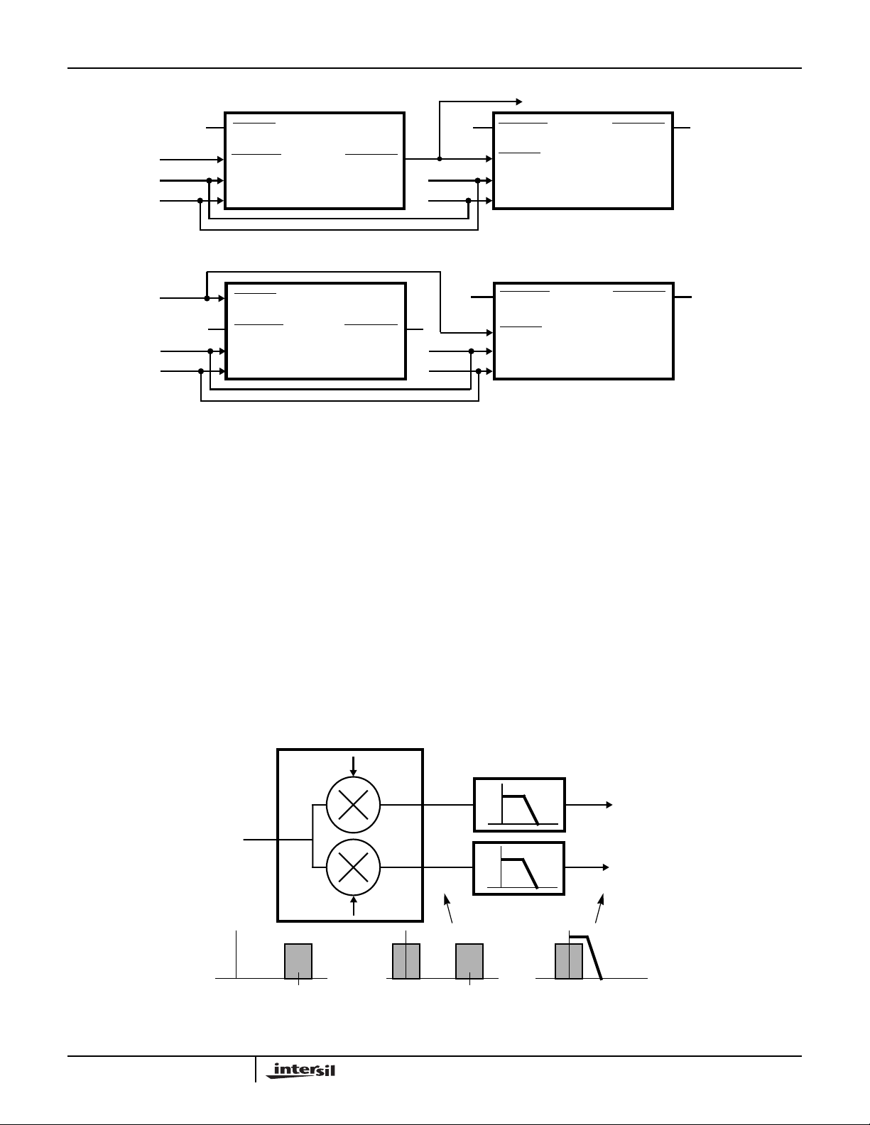
The HSP43220 is ideally suited for narrow band filtering in
Communications, Instrumentation and Signal Processing
applications. The HSP43220 provides a fully integrated
solution to high order decimation filtering.
The combination of the HSP43220 and the HSP45116
(which is a NCOM Numerically Controlled Oscillator /
Modulator) provides a complete solution to digital receivers.
The diagram in Figure 14 illustrates this concept.
The HSP45116 down converts the signal of interest to
baseband, generating a real component and an imaginary
component. A HSP43220 then performs low pass filtering
and reduces the sampling rate of each of the signals.
The system scenario for the use of the DDF involves a
narrow band signal that has been over-sampled. The signal
+5V
CK_IN
FIR_CK
+5V
CK_IN
FIR_CK
ASTARTIN STARTOUT
STARTIN
ASTARTIN STARTOUT
STARTIN
DDF
DDF
NC
is over-sampled in order to capture a wide frequency band
containing many narrow band signals. The NCOM is “tuned”
to the frequency of the signal of interest and performs a
complex down conversion to baseband of this signal, which
results in a complex signal centered at baseband. A pair of
DDFs then low pass filters the NCOM output, extracting the
signal of interest.
Design Trade-Off Considerations
Equation 2 in the Functional Description section expresses
the relationship between the number of TAPS which can be
implemented in the FIR as a function of CK_IN, FIR_CK,
H
, F
DEC
parameters. For a given speed grade and the ratio of the
clocks, and assuming minimum decimation in the HDF, the
number of FIR taps that can be implemented is given in
Equation 2.
. Table 1 provides a tradeoff of these
DEC
SAMPLED
INPUT
DAT A
3-206
HSP45116
NCOM
COS (WT)
SIN (WT)
0 10MHz 0 20MHz 0
FIGURE 14. DIGITAL CHANNELIZER
HSP43220
DDF
HSP43220
DDF

HSP43220
TABLE 1. DESIGN TRADE OFF FOR MINIMUM H
SPEEDGRADE
(MHz)
33 1 9 8 24 56 120 248
25.6 1 7 4 16 40 88 184
15 1 4 (Note) 4 16 40 88
33 2 5 10 28 64 136 280
25.6 2 4 6 20 48 104 216
15 2 2 (Note) 4 16 40 88
33 4 3 14 36 80 168 344
25.6 4 2 6 20 48 104 216
15 4 1 (Note) 4 16 40 88
33 8 2 22 52 112 232 472
25.6 8 1 6 20 48 104 216
15 8 1 6 20 48 104 216
NOTE: Filter not realizable.
FIR_CK
CK_IN MIN H
DEC
F
DEC
= 1 F
= 2 F
DEC
DEC
TAPS
= 4 F
DEC
= 8 F
DEC
DEC
= 16
DECIMATE
Intersil provides a development system which assists the
design engineer to utilizing this filter. The DECIMATE
software package provides the user with both filter design
and simulation environments for filter evaluationand design.
These tools are integrated within one standard DSP CAD
environment, The Athena Group's Monarch Professional
DSP Software package.
The software package is designed specifically for the DDF. It
provides all the filter design software for this proprietary
architecture.It provides a user-friendly menu driven interface
to allow the user to input system level filter requirements. It
provides the frequency response curves and a data flow
simulation of the specified filter design (Figure 15). It also
creates all the information necessary to program the DDF,
including a PROM file for programming the control registers.
This software package runs on an IBM™ PC™, XT™, AT™,
PS/2™ computer or 100% compatible with the following
configuration:
640K RAM
5.25” or 3.5” Floppy drive
hard disk
math co-processor
MS/PC-DOS 2.0 or higher
CGA, MCGA, EGA, VGA and
Hercules graphics adapters
For more information, see the description of DECIMATE in
the Development Tools Section of this data book.
3-207

HSP43220
3-208
FIGURE 15. DECIMATE DESIGN MODULE SCREENS

HSP43220
Absolute Maximum Ratings T
Supply Voltage. . . . . . . . . . . . . . . . . . . . . . . . . . . . . . . . . . . . . +8.0V
Input, Output or I/O Voltage Applied . . . . .GND -0.5V to VCC +0.5V
ESD Classification . . . . . . . . . . . . . . . . . . . . . . . . . . . . . . . . .Class 1
Operating Conditions
Temperature Range . . . . . . . . . . . . . . . . . . . . . . . . . . . . 0oC to 70oC
Voltage Range. . . . . . . . . . . . . . . . . . . . . . . . . . . . +4.75V to +5.25V
=25oC Thermal Information
A
Thermal Resistance (Typical, Note 1) θJA (oC/W) θJC (oC/W)
CPGA Package . . . . . . . . . . . . . . . . . . 35 5
MQFP Package . . . . . . . . . . . . . . . . . . 33 N/A
PLCC Package. . . . . . . . . . . . . . . . . . . 35 N/A
Maximum Storage Temperature Range. . . . . . . . . . -65oC to 150oC
Maximum Junction Temperature
CPGA Package . . . . . . . . . . . . . . . . . . . . . . . . . . . . . . . . . .175oC
MQFP and PLCC Package . . . . . . . . . . . . . . . . . . . . . . . . .150oC
Maximum Lead Temperature (Soldering 10s) . . . . . . . . . . . . .300oC
(MQFP, PLCC - Lead Tips Only)
Die Characteristics
Component Count . . . . . . . . . . . . . . . . . . . . . . . 193,000 Transistors
CAUTION: Stresses above those listed in “Absolute Maximum Ratings” may cause permanent damage to the device. This is a stress only rating and operationofthe
device at these or any other conditions above those indicated in the operational sections of this specification is not implied.
NOTE:
1. θJA is measured with the component mounted on an evaluation PC board in free air.
DC Electrical Specifications
PARAMETER SYMBOL TEST CONDITIONS MIN MAX UNITS
Logical One Input Voltage V
Logical Zero Input Voltage V
High Level Clock Input V
Low Level Clock Input V
Output HIGH Voltage V
Output LOW Voltage V
Input Leakage Current I
I/O Leakage Current I
Standby Power Supply Current I
Operating Power Supply Current I
CCSB
CCOP
IH
IL
IHC
ILC
OH
OL
I
O
VCC = 5.25V 2.0 - V
VCC = 4.75V - 0.8 V
VCC = 5.25V 3.0 - V
VCC = 4.75V - 0.8 V
IOH = -400µA, VCC = 4.75V 2.6 - V
IOL = +2.0mA, VCC = 4.75V - 0.4 V
VIN = VCC or GND, VCC = 5.25V -10 10 µA
V
= VCC or GND, VCC = 5.25V -10 10 µA
OUT
VIN = VCC or GND VCC = 5.25V, Note 3 - 500 µA
f = 15MHz, VIN = VCC or GND, VCC = 5.25V,
Notes 2 and 4
- 120 mA
Capacitance T
Input Capacitance C
Output Capacitance C
NOTES:
2. Power supply current is proportional to operating frequency. Typical rating for I
3. Not tested, but characterized at initial design and at major process/design changes.
4. Output load per test load circuit with switch open and CL = 40pF.
= 25oC, Note 3
A
PARAMETER SYMBOL TEST CONDITIONS MIN MAX UNITS
IN
O
FREQ = 1MHz, VCC= Open, All measurements
are referenced to device ground
CCOP
3-209
-12pF
-10pF
is 8mA/MHz.

HSP43220
AC Electrical Specifications V
= +4.75V to +5.25V, TA = 0oC to 70oC
CC
-15 -25 -33
PARAMETER SYMBOL NOTES
Input Clock Frequency F
FIR Clock Frequency F
Input Clock Period t
FIR Clock Period t
Clock Pulse Width Low t
Clock Pulse Width High t
Clock Skew Between FIR_CK
CK
FIR
CK
FIR
SPWL
SPWH
t
SK
0 15 0 25.6 0 33 MHz
0 15 0 25.6 0 33 MHz
66-39-30-ns
66-39-30-ns
26-16-13-ns
26-16-13-ns
0t
-250t
FIR
-150t
FIR
FIR
UNITSMIN MAX MIN MAX MIN MAX
-15 ns
and CK_IN
CK_IN Pulse Width Low t
CK_IN Pulse Width High t
CK_IN Setup to FIR_CK t
CK_IN Hold from FIR_CK t
RESET Pulse Width Low t
Recovery Time on RESET t
ASTARTIN Pulse Width Low t
STARTOUT Delay from CK_IN t
STARTIN Setup to CK_IN t
Setup Time on DATA_IN t
Hold Time on All inputs t
Write Pulse Width Low t
Write Pulse Width High t
Setup Time on Address Bus Before
t
CH1L
CH1H
CIS
CIH
RSPW
RTRS
AST
STOD
STIC
SET
HOLD
WL
WH
STADD
Notes 5, 8 29 - 19 - 19 - ns
Notes 5, 8 29 - 19 - 19 - ns
Notes 5, 8 27 - 17 - 17 - ns
Notes 5, 8 2 -2-2-ns
4t
CK
8t
CK
-4tCK-4tCK-ns
-8tCK-8tCK-ns
tCK+10 - tCK+10 - tCK+10 - ns
-35-20-18ns
25-15-10-ns
20-15-14-ns
0-0-0-ns
26-15-12-ns
26-20-18-ns
26-20-20-ns
the Rising Edge of Write
SetupTime on Chip Select Before the
t
STCS
26-20-20-ns
Rising Edge of Write
SetupTimeonControlBusBeforethe
t
STCB
26-20-20-ns
Rising Edge of Write
DATA_RDY Pulse Width Low t
DATA_OUT Delay Relative to
DRPWL
t
FIRDV
2t
-20-2t
FIR
-10 - 2t
FIR
-10 - ns
FIR
-50-35-28ns
FIR_CK
DATA RDY Valid Delay Relative
t
FIRDR
-35-25-20ns
to FIR_CK
DATA_OUT Delay Relative to
t
OUT
-25-20-20ns
OUT_SELH
Output Enable to Data Out Valid t
Output Disable to Data Out
OEV
t
OEZ
Note 6 - 15 - 15 - 15 ns
Note 5 - 15 - 15 - 15 ns
Three-State
Output Rise, Output Fall Times tr, t
f
from 0.8V to
-8-8-6ns
2V, Note 5
NOTES:
5. Controlled by design or process parameters and not directly tested. Characterized upon initial design and after major process and/or design
changes.
6. Transition is measured at ±200mV from steady state voltage with loading as specified in test load circuit with and CL = 40pF.
7. AC Testing is performed as follows: Input levels (CLK Input) 4.0V and 0V, Input levels (all other Inputs) 0V and 3.0V, Timing reference levels
(CLK) = 2.0V, (Others) = 1.5V, Output load per test load circuit and CL = 40pF.
8. Applies only when H_BYP = 1 or H_DRATE = 0.
3-210

AC Test Load Circuit
HSP43220
NOTE: Test head capacitance.
Timing Waveforms
t
SET
CLK_IN
DATA_IN
t
HOLD
DUT
SWITCH S1 OPEN FOR I
CCSB
C
L
AND I
S
1
(NOTE)
CCOP
I
OH
EQUIVALENT CIRCUIT
FIR_CK
t
SPWH
CLK_IN
±
1.5V I
t
FIR
t
SK
t
CHIH
OL
t
SPWL
t
CHIL
t
CK
ASTARTIN
CK_IN
STARTOUT
CK_IN
STARTIN
DATA_IN
t
AST
FIGURE 16A. FIGURE 16B.
FIGURE 16. INPUT TIMING
t
STIC
t
HOLD
t
STOD
t
SET
RESET
t
RSPW
t
RTRS
WR
AO-1
C_BUS
CS
FIGURE 17A.
FIGURE 17. START TIMING
t
t
STADD
t
STCB
t
STCS
FIGURE 17B.
WL
t
WH
t
HOLD
t
HOLD
t
HOLD
3-211

HSP43220
Timing Waveforms
FIR_CK
t
DATA_RDY
DATA_OUT
PREVIOUS OUTPUT
DATA_OUT 0-d23
FIRDR
t
FIRDV
t
r
t
DRPWL
FIGURE 18A. FIGURE 18B.
FIGURE 18C.
(Continued)
CURRENT OUTPUT
2.0V
0.8V
t
f
t
FIRDR
FIGURE 18.
DATA_OUT 16-23
OUT_SELH
OUT_ENP
OUT_ENX
t
OEV
DATA_OUT
1.7V
1.3V
t
OUT
VALID
t
OEZ
FIGURE 18D.
LOWER 8 BITSUPPER 8 BITS
All Intersil semiconductor products are manufactured, assembled and tested under ISO9000 quality systems certification.
Intersil semiconductor products are sold by description only. Intersil Corporation reserves the right to make changes in circuit design and/or specifications at any time without notice. Accordingly, the reader is cautioned to verify that data sheets are current before placing orders. Information furnished by Intersil is believed to be accurate and
reliable. However,no responsibility is assumed by Intersil or its subsidiaries for its use; nor for any infringements of patents or other rights of third parties which may result
from its use. No license is granted by implication or otherwise under any patent or patent rights of Intersil or its subsidiaries.
For information regarding Intersil Corporation and its products, see web site http://www.intersil.com
Sales Office Headquarters
NORTH AMERICA
Intersil Corporation
P. O. Box 883, Mail Stop 53-204
Melbourne, FL 32902
TEL: (407) 724-7000
FAX: (407) 724-7240
3-212
EUROPE
Intersil SA
Mercure Center
100, Rue de la Fusee
1130 Brussels, Belgium
TEL: (32) 2.724.2111
FAX: (32) 2.724.22.05
ASIA
Intersil (Taiwan) Ltd.
7F-6, No. 101 Fu Hsing North Road
Taipei, Taiwan
Republic of China
TEL: (886) 2 2716 9310
FAX: (886) 2 2715 3029
 Loading...