Intersil Corporation HSP43216 Datasheet
HSP43216
Data Sheet January 1999 File Number
Halfband Filter
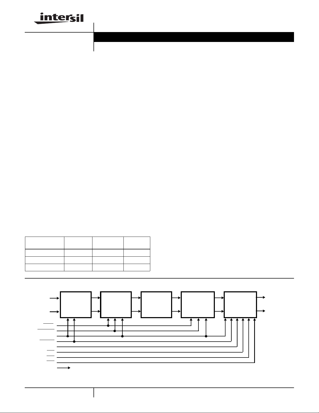
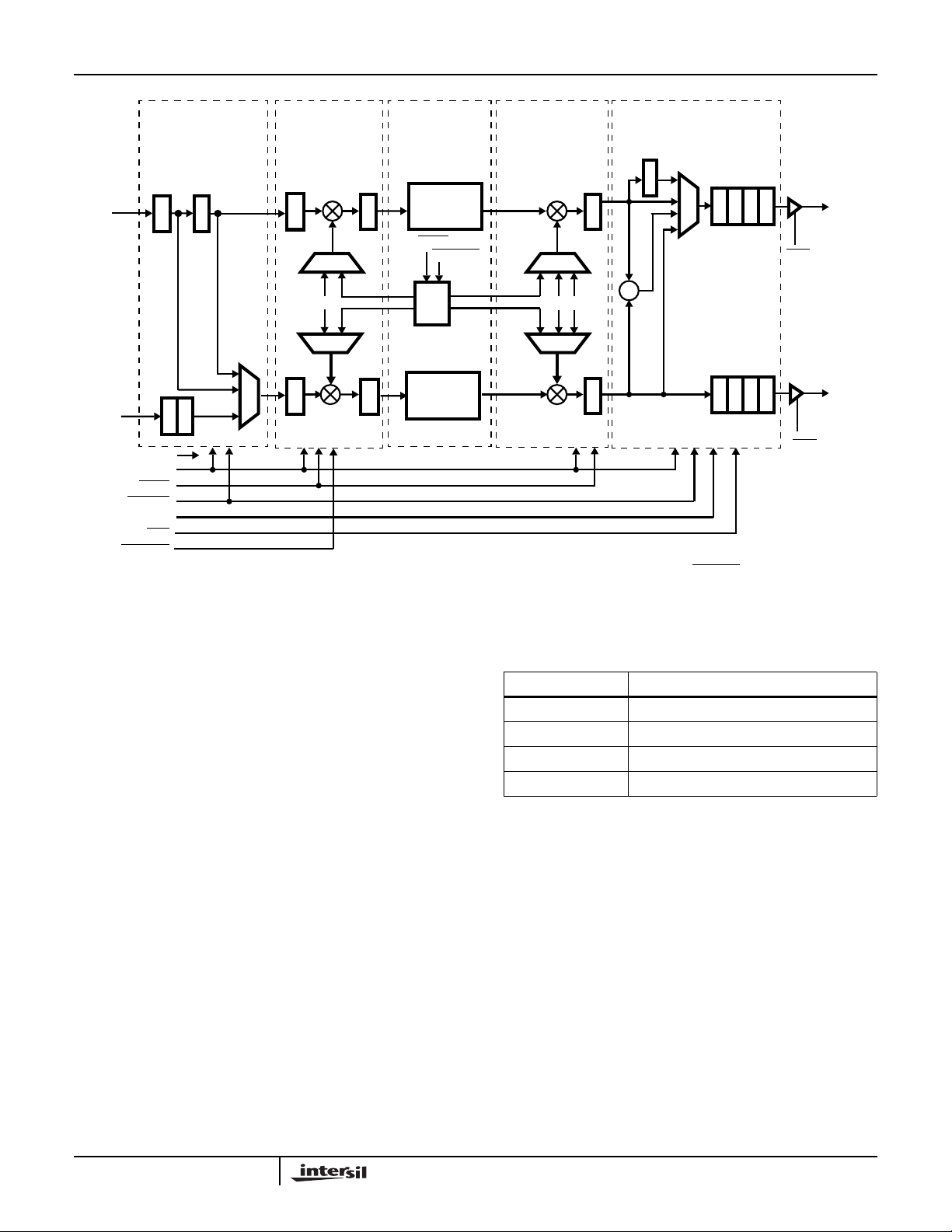
The HSP43216 Halfband Filter addresses a wide variety of
applications by combining f
quadrature up/down convert circuitry with a fixed coefficient
halfband filter processor as shown in the block diagram.
These elements may be configured to operate in one of the
four following modes: decimate by 2 filtering of a real input
signal; interpolate by 2 filtering of a real input signal; f
quadrature down conversion of a real input signal followed
by decimate-by-2 filtering to produce a complex analytic
signal; interpolate-by-2 filtering of a complex analytic signal
followed by f
/4 quadrature up conversion to produce a real
S
valued output.
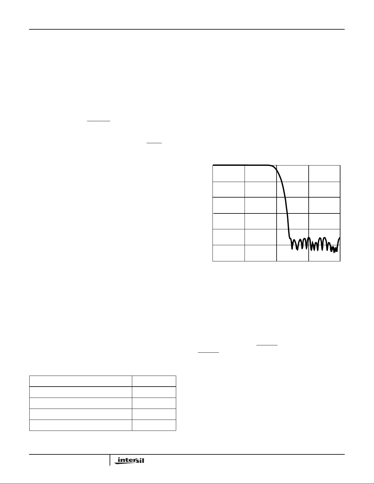
The frequency response of the HSP43216's halfband filter
has a shape factor, (passband+transition band)/passband,
of 1.24:1 with 90dB of stopband attenuation. The passband
has less than 0.0003dB of ripple from 0f
stopband attenuation of greater than 90dB from 0.3f
Nyquist. At 0.25f
the filter provides 6dB of attenuation.
S
The HSP43216 processes data streams with word widths up
to 16 bits and data rates up to 52 MSPS. The processing
throughput of the part is easily doubled to rates of up to 104
MSPS by using thepart together with an external multiplexer
or demultiplexer. Programmable rounding is provided to
support output precisions from 8 bits to 16 bits.
/4 (fS = sample frequency)
S
to 0.2fS with
S
/4
S
to
S
3365.7
Features
• Sample Rates to 52 MSPS
• Architected to Support Sample Rates to 104 MSPS Using
External Multiplexer
• Four Modes of Operation:
- Interpolate by 2 Filtering
- Decimate by 2 Filtering
- Quadrature to Real Signal Conversion
-f
/4 Quadrature Down Conversion Followed by
S
Decimate by 2 Filtering
• 16-Bit Inputs and Outputs
• 67-Tap Halfband FIR Filter with 20-Bit Coefficients
• Two’s Complement or Offset Binary Outputs
• Programmable Rounding on Outputs
• 1.24:1 Filter Shape Factor
• >90dB Stopband Attenuation
• <0.0003dB Passband Ripple
• Saturation Logic on Output
Applications
• Digital Down Conversion
Ordering Information
PART
NUMBER
HSP43216GC-52 0 to 70 85 Ld CPGA G85.A
HSP43216JC-52 0 to 70 84 Ld PLCC N84.1.15
HSP43216VC-52 0 to 70 100 Ld MQFP Q100.14x20
TEMP.
RANGE (oC)
PACKAGE
TYPE PKG. NO.
Block Diagram
f
/4
AIN0-15
BIN0-15
SYNC
USB/LSB
MODE0-1
INT/EXT
RND0-2
INPUT DATA
FLOW
CONTROLLER
FMT
OEA
OEB
CLK
S
QUADRATURE
DOWN
CONVERT
PROCESSOR
67-TAP
HALFBAND
FILTER
PROCESSOR
• D/A and A/D pre/post Filtering
• Tuning Bandwidth Expansion for HSP45116 and
HSP45106
f
/4
S
QUADRATURE
UP CONVERT
PROCESSOR
OUTPUT DATA
FLOW
CONTROLLER/
FORMATTER
AOUT0-15
BOUT0-15
3-193
CAUTION: These devices are sensitive to electrostatic discharge; follow proper IC Handling Procedures.
http://www.intersil.com or 407-727-9207
| Copyright © Intersil Corporation 1999
HSP43216
Pinouts
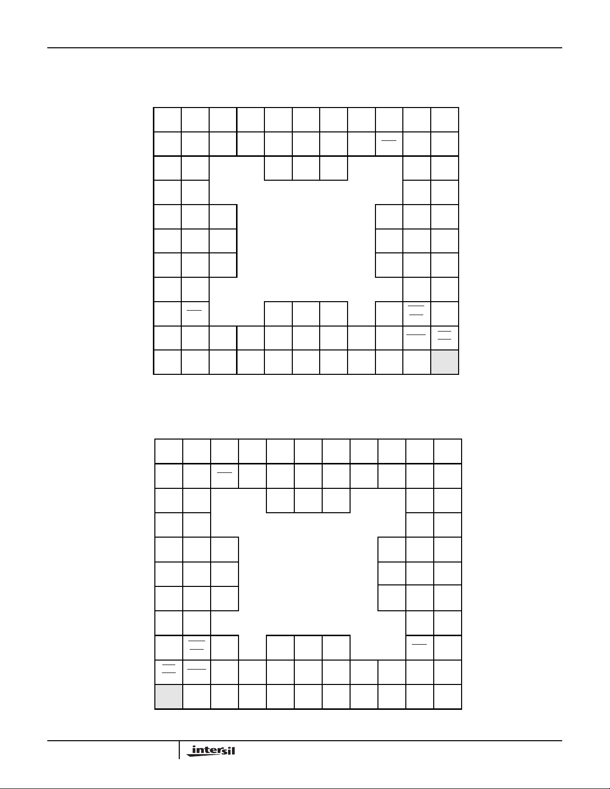
85 PIN PGA
TOP VIEW
1110987654321
BOUT BOUTBOUT BOUT
L
15 13 12 10 8
AOUT AOUT BOUT BOUT BOUT
K
2 0 14 11 9
AOUT AOUT
J
31 76 2
GND AOUT4
H
AOUT8
AOUT6
AOUT7
G
AOUT
F
10
AOUT AOUT
E
11 12 13
AOUT AOUT
D
14 15
GND
C
V
CC
B
AOUT9
AOUT5
AOUT
OEA
AIN0 AIN1 AIN4 AIN7 AIN6 AIN13
BOUT
BOUT
AIN9
GND
BOUT
BOUT
AIN10 AIN14
41
BOUT
BOUT
530
BOUT
MODE
0
BOUT
BOUT
V
CC
OEB
BIN8
BIN7
BIN3
INDEX
PIN
CLK
GND
RND2
RND0
BIN13
BIN10
BIN6
BIN4
BIN1
USB/
LSB
SYNC
RND1
BIN15
BIN14
BIN12
BIN9
BIN11
BIN5
BIN2
BIN0
INT/
EXT
L
K
J
H
G
F
E
D
C
B
A
1110987654321
MODE1AIN15AIN12AIN11AIN8AIN5AIN3AIN2FMT
GND
85 PIN PGA
BOTTOM VIEW
BOUT5
BOUT6
BOUT8GND
BOUT9
BOUT7
AIN9AIN10AIN14
10 12 13 15
BOUTBOUT
11 14
AOUT8
AOUT6
AOUT9
AOUT5
AOUT
AOUT
OEA
AIN0AIN1AIN4AIN7AIN6AIN13
RND1
L
RND2
BIN15
K
BIN14
BIN12
BIN9
BIN11
BIN5
BIN2
BIN0
INT/
EXT
RND0
BIN13
BIN10
BIN6
BIN4
BIN1
USB/
LSB
SYNC
J
H
G
F
E
D
C
B
CC
OEB
BIN8
BIN7
BIN3
INDEX
PIN
CLK
BOUT0
BOUT1
V
GND
BOUT4
BOUT3
BOUT2
MODE
V
CC
1110987654321
BOUTBOUT BOUTBOUT
AOUT2AOUT0
AOUT3AOUT1
GNDAOUT4
AOUT7
AOUT
10
AOUT
1213
AOUTAOUT
15 14
GND
V
CC
11
A
PIN ‘A1’
ID
L
K
J
H
G
F
E
D
C
B
A
PIN ‘A1’
ID
V
3-194
CC
MODE1 AIN15 AIN12 AIN11 AIN8 AIN5 AIN3 AIN2 FMT
GND
A
1110987654321
HSP43216
Pinouts
(Continued)
V
CC
NC
NC
NC
NC
SYNC
USB/LSB
INT/EXT
BIN0
BIN1
BIN2
BIN3
BIN4
BIN5
BIN6
BIN7
BIN8
BIN9
BIN10
BIN11
BIN12
BIN13
BIN14
BIN15
RND0
RND1
NC
NC
NC
NC
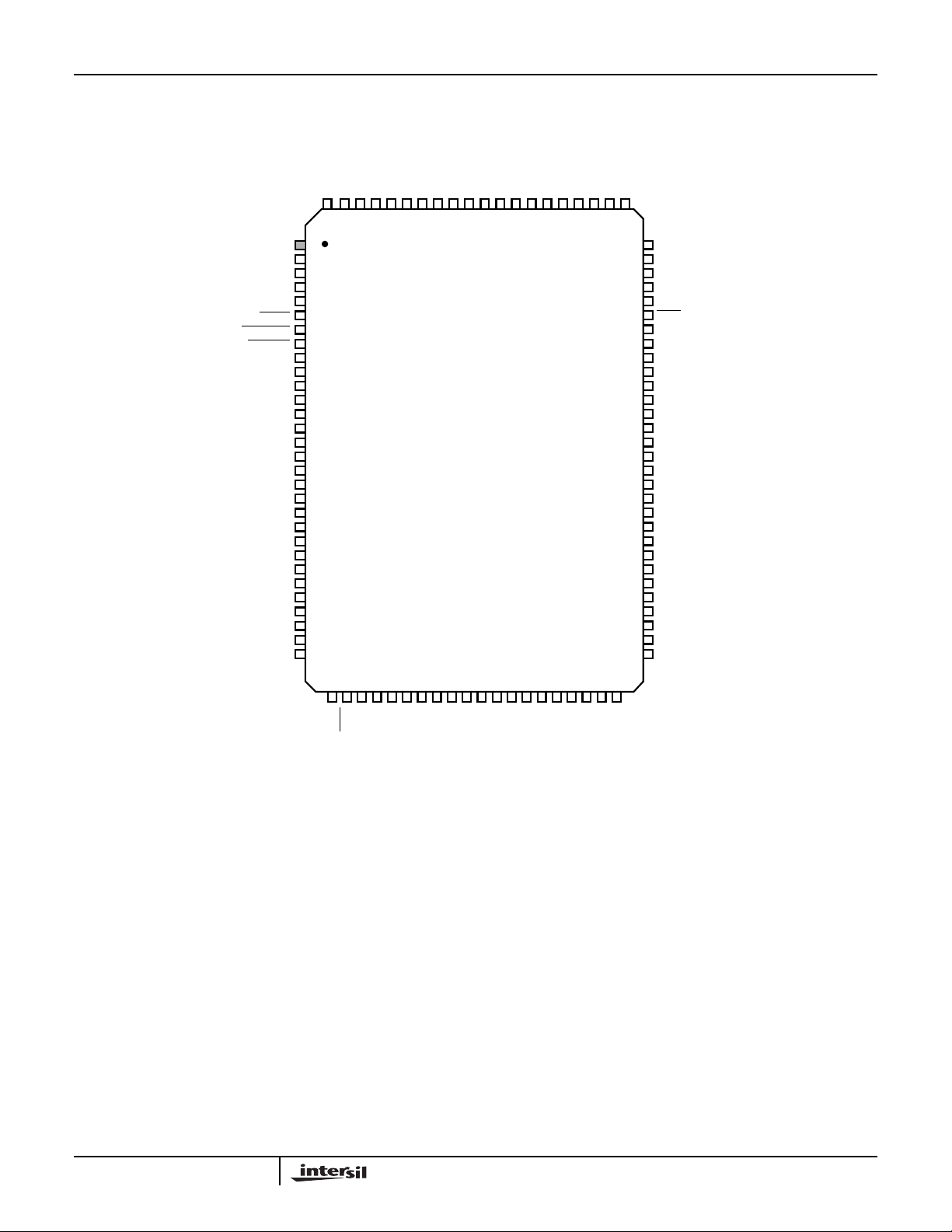
100 LEAD MQFP
TOP VIEW
AIN0
AIN1
AIN2
AIN3
AIN9
AIN8
AIN15
AIN14
AIN13
AIN12
GND
MODE1
CLK
1
2
3
4
5
6
7
8
9
10
11
12
13
14
15
16
17
18
19
20
21
22
23
24
25
26
27
28
29
30
MODE0
99 98 97 96 95 94 93 91 89 87 85 84 83 818286889092100
AIN10
AIN11
AIN7
AIN6
AIN5
AIN4
80
NC
79
NC
78
NC
77
NC
76
FMT
75
OEA
74
V
CC
73
GND
72
AOUT15
71
AOUT14
70
AOUT13
69
AOUT12
68
AOUT11
67
AOUT10
66
AOUT9
65
AOUT8
64
AOUT7
63
AOUT6
62
AOUT5
61
GND
60
AOUT4
59
AOUT3
58
AOUT2
57
AOUT1
56
AOUT0
55
NC
54
NC
53
NC
52
NC
BOUT15
51
32 33 3435 36 37 38 40 42 44 46 47 48 50494543413931
OEB
RND2
GND
CC
V
BOUT1
BOUT0
BOUT3
BOUT2
BOUT5
BOUT4
BOUT7
BOUT6
BOUT9
BOUT8
GND
BOUT10
BOUT12
BOUT11
BOUT14
BOUT13
3-195
HSP43216
Pinouts
(Continued)
SYNC
USB/LSB
INT/EXT
BIN0
BIN1
BIN2
BIN3
BIN4
BIN5
BIN6
BIN7
BIN8
BIN9
BIN10
BIN11
BIN12
BIN13
BIN14
BIN15
RND0
RND1
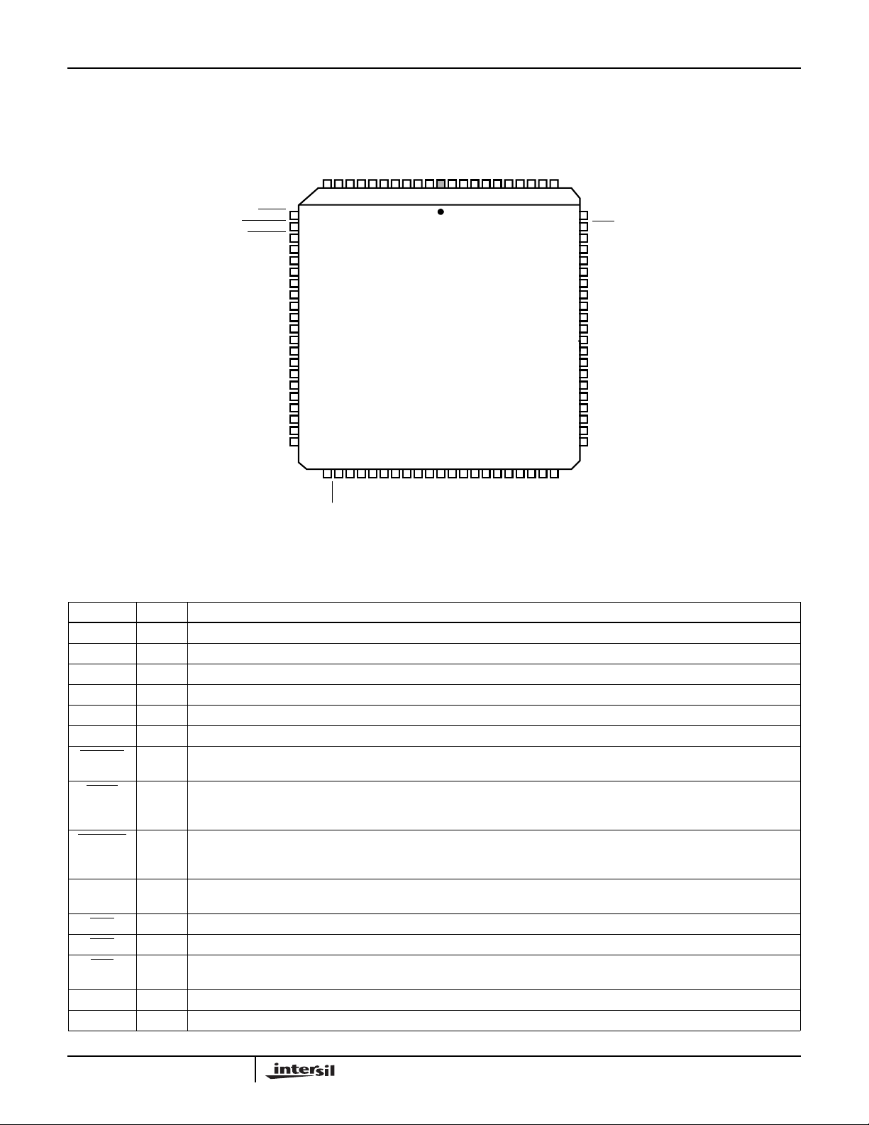
84 LEAD PLCC
TOP VIEW
AIN7
AIN6
GND
BOUT9
AIN4
AIN5
BOUT11
BOUT10
AIN9
AIN15
AIN14
AIN13
BOUT2
BOUT1
AIN12
BOUT4
BOUT3
GND
MODE1
OEB
GND
MODE0
CC
V
BOUT0
VCCCLK
111098765432184838281807978777675
12
13
14
15
16
17
18
19
20
21
22
23
24
25
26
27
28
29
30
31
32
33 34 3536 37 3839 4041 42 4344 45 4647 4849 50 5152 53
RND2
AIN10
AIN11
BOUT7
BOUT6
BOUT5
AIN8
BOUT8
AIN1
AIN2
AIN3
BOUT14
BOUT13
BOUT12
AIN0
74
73
72
71
70
69
68
67
66
65
64
63
62
61
60
59
58
57
56
55
54
BOUT15
FMT
OEA
V
CC
GND
AOUT15
AOUT14
AOUT13
AOUT12
AOUT11
AOUT10
AOUT9
AOUT8
AOUT7
AOUT6
AOUT5
GND
AOUT4
AOUT3
AOUT2
AOUT1
AOUT0
Pin Description
NAME TYPE DESCRIPTION
V
CC
GND - Ground.
CLK I Clock Input. (CMOS LEVEL). fS is the frequency of CLK
AIN0-15 I Input Data Bus A. AIN0 is the LSB. Input data format is 16-bit Two’s Complement.
BIN0-15 I Input Data Bus B. BIN0 is the LSB. Input data format is 16-bit Two’s Complement.
MODE0-1 I The Mode Select Inputs set one of four operational modes as highlighted in Table 1.
INT/EXT I The Internal\External multiplexer select inputs set whether the data multiplex/demultiplex function required in the various
SYNC I This input is used to synchronize the input sample stream with the zero degree phase of the up or down convert Local
USB/LSB I The Upper and Lower Sideband select line is used to specify the direction of frequency translation imparted on the data
RND0-2 I The Round Select inputs set the number of output bits from eight (RND = 000) to sixteen (RND = 110). Least significant
OEA I Three-State Control Output Bus A, OUTA0-15. Active Low.
OEB I Three-State Control Output Bus B, OUTB0-15. Active Low.
FMT I The Format select input is used to convert the two’s complement output to offset binary (unsigned). When asserted high,
AOUT0-15 O Output Bus A. AOUT0 is the LSB.
BOUT0-15 O Output Bus B. BOUT0 is the LSB.
- +5V Power.
operational modes is performed internally (High State) or externally to the chip (Low State).
Oscillators. In the straightdecimatemodes, this input can be use tosynchronize the input sample stream with aparticular
phase of the halfband filter. (See the Operational Modes Section for additional information).
stream in the Down Convert and Decimate Mode and in the Quadrature to Real Convert Mode. (See Operational Modes
Section for additional information).
output bits are zeroed. See Table 4.
the AOUT15 and BOUT15 bits are inverted from the normal two’s complement representation.
3-196
HSP43216
AIN0-15
BIN0-15
MODE0-1
USB/LSB
INPUT DATA FLOW
CONTROLLER
R
E
G
R
R
E
E
G
G
CLK
SYNC
INT/EXT
RND0-2
FMT
/4 QUADRATURE
f
S
DOWN CONVERT
R
E
G
M
U
X
R
E
G
MUX
1,-1,1,..
1
1
-1,1,-1,.
MUX
R
E
G
67-TAP HALFBAND
PROCESSOR
PIPELINE
† DELAY 2 - 35
††
R
E
G
††
R
E
G
EVEN TAP
SYNC
f
† DELAY 19
ODD TAP
FILTER
FILTER
USB/LSB
/4
S
L.O.
PIPELINE
FILTER
/4 QUADRATURE
f
S
UP CONVERT
MUX
...,2,-2,2
..,-2,2,-2
MUX
OUTPUT DATA FLOW
CONTROLLERPROCESSORPROCESSOR
R
†
R
E
G
1
2
1
2
E
G
M
R
F
U
X
R
N
M
E
D
T
G
R
E
G
AOUT0-15
OEA
+
†
R
E
G
BOUT0-15
OEB
R
F
R
E
G
R
N
M
E
D
G
T
† Indicates elements which operate at CLK/2 when the INT/EXT control input is high.
FIGURE 1. HALFBAND BLOCK DIAGRAM
Functional Description
The operation of the HSP43216 centers around a fixed
coefficient, 67-Tap, Halfband Filter Processor as shown in
Figure 1. The Halfband Filter Processor operates stand
alone to provide two fundamental modes of operation:
interpolate or decimate by two filtering of a real signal. In two
other modes, the Quadrature Up/Down Convert circuitry
operates together with the Filter Processor block to provide
f
/4 Down Conversion with decimate by 2 filtering or
S
Quadrature to Real Conversion.
In Down Convert and Decimate mode, a real input sample
stream is spectrally shifted by f
resulting complex signal is then halfband filtered and
decimated by 2 to produce real and imaginary output
samples at half of the input data rate.
In Quadrature to Real Conversion mode, the real and
imaginary components of aquadratureinput are interpolated
by two and halfband filtered. The filtered result is then
spectrally shifted by f
/4 and the real component of this
S
operation is output at twice the input sample rate.The
HSP43216 is configured for different operational modes by
setting the state of the mode control pins, MODE1-0 as
shown in Table 1.
/4. Each component of the
S
TABLE 1. MODE SELECT TABLE
MODE1-0 MODE
00 Decimate by Two
01 Interpolate by Two
10 Down Convert and Decimate
11 Quadrature to Real Conversion
Input Data Flow Controller
The Input Data FlowControllerroutesdatasamplesfromthe
AIN0-15 and BIN0-15 inputs to the internal processing
elements of the Halfband. The data routing paths are based
on mode of operation and are more fully discussed in the
Operational Modes section.
fS/4 Quadrature Down Convert Processor
The fS/4 QuadratureDownConvert Processor operatesasa
Quadrature LO which provides the negative f
shift required to center the upper sideband of a real input
signal at DC. This operation is equivalent to multiplying the
real sample stream, x(n), by the quadrature components of
the complex exponential e
⁄()–
j πn2
xn()e
xn() πn2⁄()jx n() π– n2⁄()sin+cos=
-j(π/2)n
as given below:
/4 spectral
S
(EQ. 1)
3-197
HSP43216
For added flexibility, a spectrally reversed version of the
above process may be realized by configuring the Down
Convert processor to impart a positive f
/4 spectral shift on
S
the input signal. This has the effect of centering the lower
sideband of the input signal at DC and is achieved by
reversing the sign of the sine term in the quadrature mix as
shown below:
xn()e
x n() πn2⁄()jx n() πn2⁄()sin+cos=
(EQ. 2)
⁄()
j πn2
The direction of the spectral shift imparted by the Down
Convert Processor is set by the Upper Sideband/ Lower
Sideband control input,
-f
/4 spectral shift is used to center the input signal’s upper
S
sideband at DC. When asserted low, a spectral shift of f
is used to center the lower sideband at DC. The
USB/LSB. When this input is high, a
/4
S
SYNC
control input may be used to synchronize the incoming data
stream with the zero degree phase of the complex
exponential as described in the Operational Modes section.
The real and imaginary sample streams generated by the
down convert operation are passed to the Halfband Filter
block on the upper and lower processing legs respectively.
The Down Convert Processor is only active in Down Convert
and Decimate Mode, MODE1-0 = 10. In the other modes,
the data on the upper and lower processing legs pass
unaltered.
67-Tap Halfband Filter Processor
The processing required to implement the 67-Tap Halfband
filter is distributed across two polyphase branches
comprised of even and odd tap filters as shown in Figure 1.
The Even Tap Filter performs a filtering operation using the
even indexed coefficients (even phase) of the halfband filter.
The Odd Tap Filter uses the odd indexed coefficients (odd
phase) of the halfband filter.
processing reduces to a delayandscaleoperationsince
the center tap is the only non-zero odd tap for a
halfband filter.
Together the polyphase filters perform the
sum of-products required to implement the 67-tap halfband
filter in an architecture capable of supporting a variety of
operational modes. The frequency response of the halfband
filter is given graphically in Figure 2 and in tabular form in
Table 3. Table 2 shows the different modes and the related
frequency with which the spectra in Figure 2 is normalized.
TABLE 2. NORMALIZED FREQRUENCY vs MODE
MODE f
Decimate by Two CLK
Interpolate by Two CLK/2
NOTE: the odd tap filter’s
S
The polyphase implementation of the halfband filter
provides the flexibility to realize a variety of filter
configurations. In Decimate by Two Mode, the outputs of
the each polyphase branch are summed to yield the filter
output. In Interpolate by Two mode, the polyphase filters
produce independent outputs which are multiplexed into a
single sample stream at the interpolated data rate. In the
Up Convert and Down Convert Modes, the polyphase
branches filter the real and imaginary components of a
complex sample stream with the equivalent of identical 67Tap Halfband Filters. For these modes, the real component
is processed by the Even Tap filter and the imaginary
component is processed by the Odd Tap filter. The
Operational Modes Section provides further details
regarding the data flow and operation of the Filter
Processor for the various modes.
0
-20
-40
-60
-80
MAGNITUDE (DB)
-100
-120
0f
NORMALIZED FREQUENCY
FIGURE 2. FREQUENCY RESPONSE OF 67-TAP HALFBAND
FILTER
/4 FS/2
S
3fS/8fS/8
As a standard DSP term, group delay is defined as the time
it takes to obtain valid filtered data given a certain input
pattern. Both the Even Tap and Odd Tap filters have an
identical group delay of 19 clocks relative to the operating
mode of the halfband. The group delayhasbeenspecifiedin
the data flow diagrams following this section. The delay
clocks equal CLK when
INT/EXT = 0 and CLK/2 when
INT/EXT = 1.
NOTE: Pipeline delay specifies the time it takes for bits to
toggle at the output given a certain input pattern. The Odd tap
filter has a pipeline delay of 19 CLKs with respect to the
operating mode because itconsists of only the center tapofthe
67-tap halfband. The Even tap filter has a pipeline delayof2-35
CLKs with respect to the operating mode.
Down Convert and Decimate CLK
Quadrature to Real CLK/2
3-198
 Loading...