

Intersil Corporation HSP43168-883 Datasheet

HSP43168/883
Data Sheet May 1999
Dual FIR Filter
The HSP43168/883 Dual FIR Filter consists of two
independent 8-tap FIR filters. Each filter supports
decimation from 1 to 16 and provides on-board storage for
32 sets of coefficients. The Block Diagram shows two FIR
cells each fed by a separate coefficient bank and one of two
separate inputs. The outputs of the FIR cells are either
summed or multiplexed by the MUX/Adder. The compute
power in the FIR Cells can be configured to provide
quadrature filtering, complex filtering, 2-D convolution, 1D/2-D correlations, and interpolating/decimating filters.
The FIR cells take advantage of symmetry in FIR
coefficients by pre-adding data samples prior to
multiplication. This allows an 8-tap FIR to be implemented
using only 4 multipliers per filter cell. These cells can be
configured as either a single 16-tap FIR filter or dual 8-tap
FIR filters. Asymmetric filtering is also supported.
Decimation ofup to 16 is providedto boostthe effectivenumber
of filter taps from 2 to 16 times. Further, the Decimation
Registers provide the delay necessary for fractional data
conversion and 2-D filtering with kernels to 16 x 16.
The flexibility of the dual is further enhanced by 32 sets of
user programmable coefficients. Coefficient selection may
be changed asynchronously from clock to clock. The ability
to toggle between coefficient sets further simplifies
applications such as polyphase or adaptive filtering.
The HSP43168 is a low power fully static design
implemented in an advanced CMOS process. The
configuration of the device is controlled through a standard
microprocessor interface.
File Number
3177.3
Features
• This Circuit is Processed in Accordance to MIL-STD-883
and is Fully Conformant Under the Provisions of
Paragraph 1.2.1.
• Two Independent 8-Tap FIR Filters Configurable as a
Single 16-Tap FIR
• 10-Bit Data and Coefficients
• On-Board Storage for 32 Programmable
Coefficient Sets
• Up To: 256 FIR Taps, 16 x 16 2-D Kernels, or
10 x 20-Bit Data and Coefficients
• Programmable Decimation to 16
• Programmable Rounding on Output
• Standard Microprocessor Interface
• 33MHz, 25.6MHz Versions
Applications
• Quadrature, Complex Filtering
• Correlation
• Image Processing
• PolyPhase Filtering
• Adaptive Filtering
Ordering Information
TEMP.
PART NUMBER
HSP43168GM-25/883 -55 to 125 84 Ld PGA G84.A
HSP43168GM-33/883 -55 to 125 84 Ld PGA G84.A
RANGE (oC) PACKAGE
PKG.
NO.
Block Diagram
INA0 - 9
INB0 - 9/
OUT0 - 8
OEL
OEH
10
10
CIN0 - 9
A0 - 8
WR
CSEL0 - 4
1
MUX
10
9
COEFFICIENT
BANK A
FIR CELL A
CAUTION: These devices are sensitive to electrostatic discharge; follow proper IC Handling Procedures.
MUX
MUX/
ADDER
919
http://www.intersil.com or 407-727-9207
COEFFICIENT
BANK B
FIR CELL B
CONTROL/
CONFIGURATION
OUT9 - 27
| Copyright © Intersil Corporation 1999
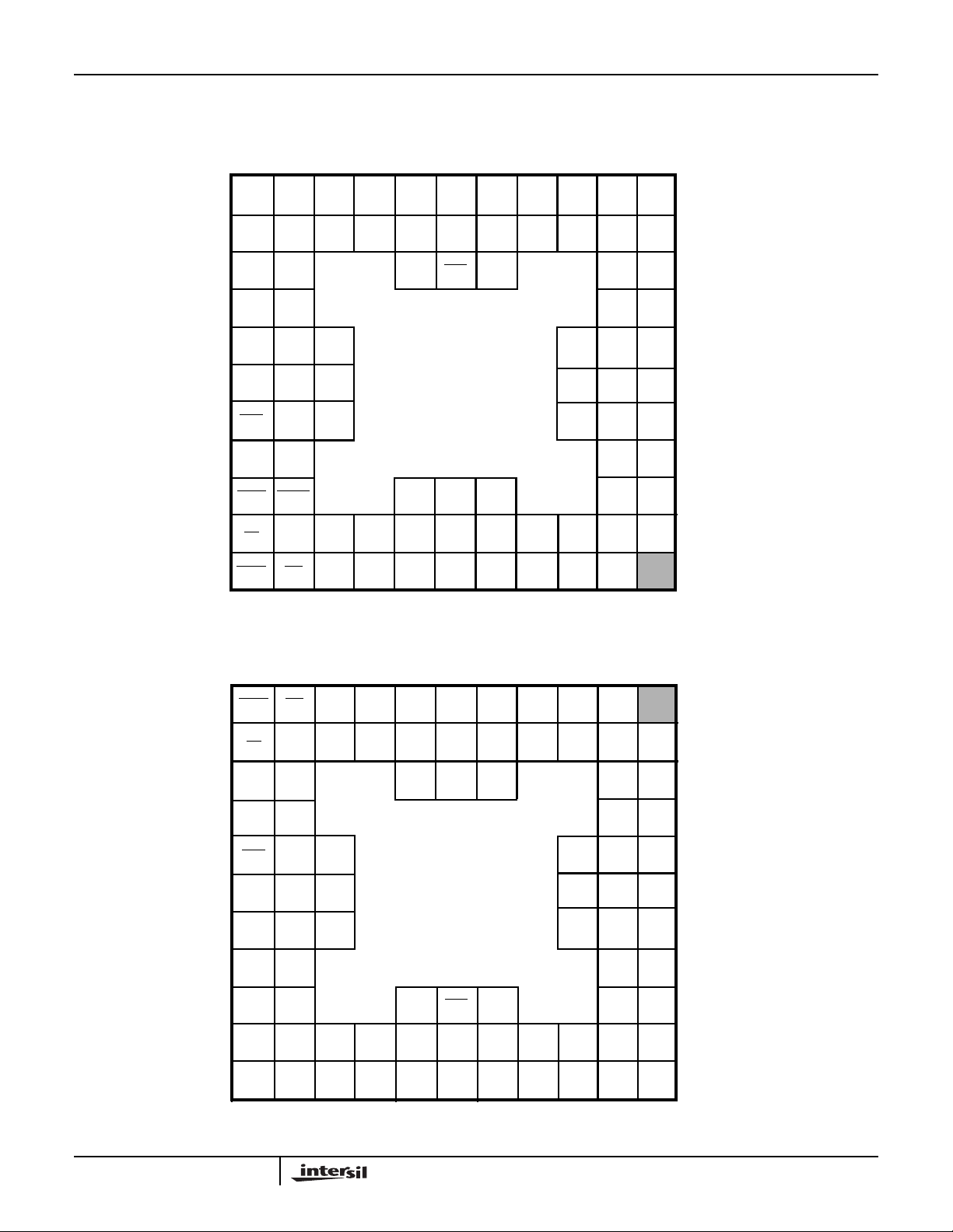
Pinouts
HSP43168/883
84 PIN PGA
TOP VIEW
11 10 9 8 7 6 5 4 3 2 1
GND OUT15
L
OUT18
K
OUT19
J
OUT21
H
OUT24 OUT23 OUT25
G
OUT27 OUT22 OUT26
F
OEH
E
V
D
CC
C
SHFT
B
EN
RVRS WR
A
111098 7654321
OUT14 OUT12 OUT10 OUT11
OUT13
OUT16
V
CC
OUT20
CLK
GND
ACCEN
FWRDTXFR
MUX0 MUX1
A0
GND
V
CC
OUT9
A5
A4A1
INB1 INB4 INB5 INB6
INB0
INB3 INA2
OEL
INA7 INA5
INA8 INA9
CIN2 CIN1
CSEL0
A6
A2A3
A7 CSEL1
A8
CC
CSEL2 CIN9V
CSEL3 CSEL4
INB8
INA0OUT17
INA3 INA4
GND
CIN6 CIN4
CIN7
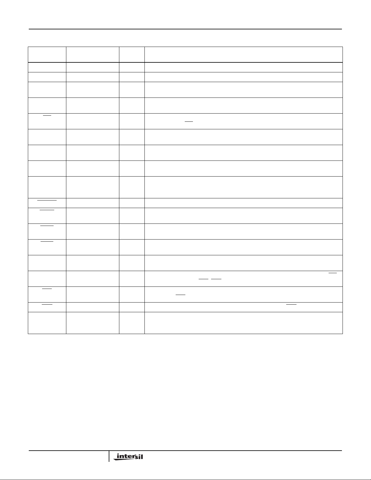
84 PIN PGA
BOTTOM VIEW
1110987654321
CSEL2 CIN9V
CSEL3 CSEL4
CIN7
A
RVRS WR
SHFT
B
EN
GND
MUX0 MUX1
A0
A7 CSEL1
A4A1
A2A3
A8
CC
INB9
INA1INB7GNDINB2
INA6
V
CC
CIN0
CIN3
CIN5
CIN8
CIN8
CIN5
L
K
J
H
G
F
E
D
C
B
PIN 'A1'
A
PIN 'A1'
A
B
ID
ID
TXFR
C
D
E
F
G
H
J
K
L
FWRD
ACCEN
V
CC
OEH GND CLK
OUT27 OUT22 OUT26
OUT24 OUT23 OUT25
OUT21 OUT20
OUT19 OUT17
V
OUT18
GND
CC
OUT15 OUT14 OUT12 OUT10 OUT11
1110987654321
OUT16
OUT13
A5
OUT9
V
CC
CSEL0
A6
INB3 INA2
OEL
INB0
INB1 INB4 INB5 INB6
CIN6 CIN4
GND
CIN2 CIN1
INA8 INA9
INA7 INA5
INA3 INA4
INA0
INB8
2
CIN3
CIN0
V
CC
INA6
INA1INB7GNDINB2
INB9
C
D
E
F
G
H
J
K
L
HSP43168/883
Pin Description
PIN
NAME
V
CC
GND A9, E10, L11, K4, D2 Ground.
CIN0-9 E1-3, D1, C1-2, B1-3,
A0-8 A5-8, B6-8, C6-7 I Control/Coefficient Address Bus. Processorinterface for addressing control and Coefficient
WR A10 I Control/Coefficient Write Clock. Datais latched intothe Control andCoefficient Registers on
CSEL0-4 A2-4, B4, C5 I Coefficient Select. This input determines which of the 32 coefficient sets are to be used by
INA0-9 K1, J1-2, H1-2, G1-3,
INB0-9 L1-5, K2-3, K5-6, J5 I/O Bidirectional Input for FIR B. INB0 is the LSB and is input only. When used as output,
OUT9-27 F9-11,G9-11, H10-11,
SHFTEN B11 I Shift Enable. Thisactive low inputenables shifting ofdata through theDecimation Registers.
FWRD C10 I Forward ALU Input Enable. When active low, data from the forward decimation pathis input
RVRS A11 I Reverse ALUInput Enable. When active low, data from the reversedecimation pathis input
TXFR C11 I Data Transfer Control. This active low input switches the LIFO being read into the reverse
MUX0-1 B9-10 I Adder/Mux Control. This input controls data flow through the output Adder/Mux. Table 3.0
CLK E9 I Clock. All inputs except those associated with the processor interface (CIN0-9, A0-8, WR)
OEL J6 I Output Enable Low. This tristate control enables the LSB’s of the output bus to
OEH E11 I Output Enable High. This tristate control enables OUT9-27 when OEH is low.
ACCEN D10 I Accumulate Enable. This activehigh inputallows accumulation inthe FIRCell Accumulator.
NUMBER TYPE DESCRIPTION
B5, D11, K10, K7, F1 VCC: +5V power supply pin.
I Control/Coefficient Data Bus. Processor interface for loading control data and coefficients.
A1
F2-3
J10-11, J7, K11, K8-9,
L6-10
CIN0 is the LSB.
Registers. A0 is the LSB.
the rising edge of WR.
FIR A and B. This input is registered and CSEL0 is the LSB.
I Input to FIR A. INA0 is the LSB.
INB1-9 is the LSB’s of the output bus.
O 19MSB’s of Output Bus.Data format is either unsigned or two’s complement depending on
configuration. OUT27 is the MSB.
to the ALU’s through the “a” input. When high, the “a” inputs to the ALUs are zeroed.
to the ALU’s through the “b” input. When high, the “b” inputs to the ALUs are zeroed.
decimation path withthe LIFO beingwritten from the forward decimationpath (see Figure1).
lists the various configurations.
and the output enables (OEL, OEH) are registered by the rising edge of CLK.
INB1-9 when OEL is low.
A low on this input latches the FIR Accumulator contents into the Output Holding Registers
while zeroing the feedback path in the accumulator.
3
 Loading...