Intersil Corporation HSP43124 Datasheet

HSP43124
Data Sheet May 1999
Serial I/O Filter
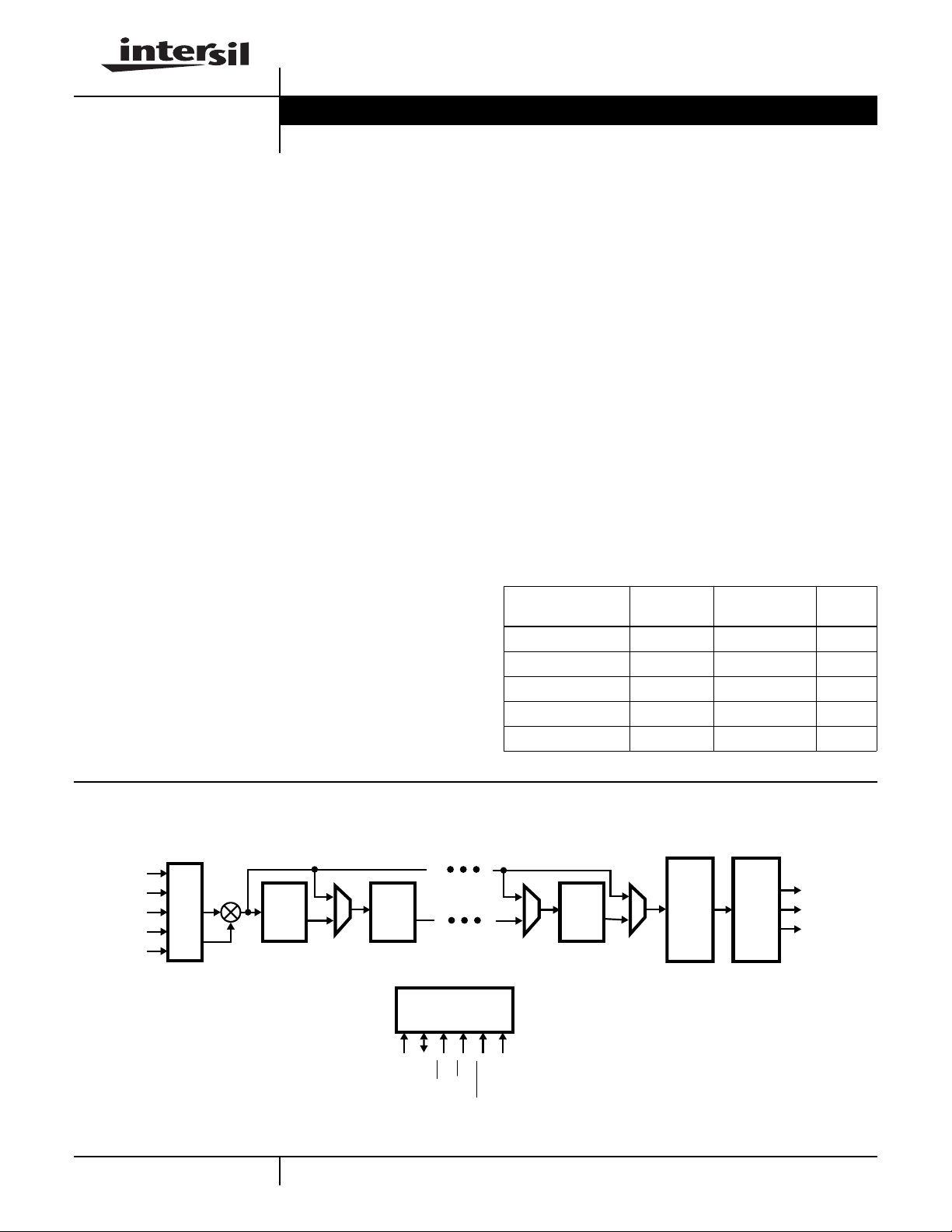
The Serial I/O Filter is a high performance filter engine that is
ideal for off loading the burden of filter processing from a
DSP microprocessor. It supports a variety of multistage filter
configurations based on a user programmablefilterandfixed
coefficient halfband filters. These configurations include a
programmable FIR filter of up to 256 taps, a cascade of from
one to five halfband filters, or a cascade of halfband filters
followed by a programmable FIR. The half band filters each
decimate by a factoroftwo, and the FIR filter decimates from
one to eight. When all six filters are selected, a maximum
decimation of 256 is provided.
For digital tuning applications, a separate multiplier is
provided which allows the incoming data stream to be
multiplied, or mixed, by a user supplied mix factor. A two pin
interface is provided for serially loading the mix factor from
an external source or selecting the mix factor from an onboard ROM. The on-board ROM contains samples of a
sinusoid capable of spectrally shifting the input data by one
quarter of the sample rate, F
function as a digital down converter when the filter stages
are configured as a low-pass filter.
The serial interface for
3-
with the serial ports of common DSP microprocessors.
Coefficients and configuration data are loaded over a
bidirectional eight bit interface.
/4. This allows the chip to
S
input and output data is compatible
File Number
3555.6
Features
• 45MHz Clock Rate
• 256 Tap Programmable FIR Filter
• 24-Bit Data, 32-Bit Coefficients
• Cascade of up to 5 Half Band Filters
• Decimation from 1 to 256
• Two Pin Interface for Down Conversion by F
/4
S
• Multiplier for Mixing or Scaling Input with an External
Source
• Serial I/O Compatible with Most DSP Microprocessors
Applications
• Low Cost FIR Filter
• Filter Co-Processor
• Digital Tuner
Ordering Information
TEMP.
PART NUMBER
HSP43124PC-45 0 to 70 28 Ld PDIP E28.6
HSP43124PC-33 0 to 70 28 Ld PDIP E28.6
HSP43124SC-45 0 to 70 28 Ld SOIC M28.3
HSP43124SC-33 0 to 70 28 Ld SOIC M28.3
HSP43124SI-40 -40 to 85 28 Ld SOIC M28.3
RANGE (oC) PACKAGE
PKG.
NO.
Block Diagram
DIN
SCLK
SYNCIN
MXIN
SYNCMX
INPUT
FORMATTER
HALF
BAND
FILTER
1
FORMATTER
DOUT
SYNCOUT
CLKOUT
HALF
BAND
#1
FILTER
#2
CONTROL
INTERFACE
RD
WR
A0-2
C0-7
CAUTION: These devices are sensitive to electrostatic discharge; follow proper IC Handling Procedures.
FCLK
FSYNC
http://www.intersil.com or 407-727-9207
HALF
BAND
FILTER
#5
FIR
FILTER
PROGRAMMABLE
| Copyright © Intersil Corporation 1999
OUTPUT

Pinout
SCLK
SYNCIN
GND
MXIN
SYNCMX
FSYNC
V
CC
FCLK
WR
RD
A0
A1
A2
V
CC
HSP43124
28 LEAD PDIP, SOIC
1
2
3
4
5
6
7
8
9
10
11
12
13
14
TOP VIEW
28
27
26
25
24
23
22
21
20
19
18
17
16
15
DIN
DOUT
SYNCOUT
CLKOUT
V
CC
C7
C6
C5
C4
GND
C3
C2
C1
C0
2

HSP43124
Pin Description
NAME TYPE DESCRIPTION
V
CC
GND - Ground
DIN I Serial Data Input. Thebitvalue present on thisinputis sampled on therisingedgeof SCLK. A “HIGH”onthis input
SYNCIN I Data Sync.TheHSP43124 issynchronizedto the beginningof a newdata word onDIN when SCLKsamplesSYN-
SCLK I Serial Input CLK. The rising edge of SCLK clocks data on DIN and MXIN into the part. The following signals are
MXIN I Mix FactorInput.MXINistheserial input forthemixfactor.ItissampledontherisingedgeofSCLK.A“HIGH”on
SYNCMX I Mix Factor Sync. The HSP43124 is synchronized to the beginning of a serially input mix factor when SCLK samples
FCLK I Filter Clock. The filter clock determines the processing speed of the Filter Compute Engine. Clock rate require-
FSYNC I Filter Sync. This input, when sampled low by the rising edge of FCLK, resets the filter compute engine so that the
- +5V Power Supply
represents a “1”, and a low onthisinputrepresents“0”.Theword format and operation of serial interfacearecontained in the Data Input Section.
CIN “HIGH” one SCLKbefore the first bitofthenew word.
for longer than one SCLK cycle.
synchronous to this clock: DIN, SYNCIN, MXIN, SYNCMX.
this input representsa“1”, and a low onthisinputrepresents “0”. Also used to specifytheWeaver Modulator ROM
output asapart ofthetwo pin FS/4 downconversioninterface.Detailson word format andoperationare contained
in the Mix Factor Section.
SYNCMX “HIGH”one SCLK beforethefirst bit ofthenew mixf actor.
one SCLK cycle.Also used to specify WeaverModulator ROM output as a part of the two pin FS/4 down conversion interface.
ments on FCLK for particular filter configurations is discussed in the Filter Compute Engine Section. This clock
may be asynchronous to the serial input clock (SCLK). FSYNC is synchronous to this clock.
data sample following the next SYNCIN cycle is the first data sample into the filter structure. If a data stream is
currently beinginput,the current sum ofproductsand the input dataare“canceled” and the DINpinis ignored until
the next SYNCIN cycle occurs.
NOTE: SYNCINshouldnotmaintaina “HIGH” state
NOTE: SYNCMXshould only pulse“HIGH”for
WR I Write. The falling edge of WR loads data present on C0-7 into the configuration orcoefficientregisterspecifiedby
the address on A0-2. The WR signal is asynchronous to all other clocks.
RD is low.
RD I Read. The falling edge of RD accesses the control registers or coefficient RAM addressed by A0-2 and places
the contents of thatmemory location onC0-7.WhenRD returns “HIGH” the C0-7busfunctions as an input bus.
The RD pin is asynchronous to all other clocks.
A0-2 I Address Bus. The A0-2 inputs are decoded on the falling edge of both RD and WR. Table 1 shows the address
map for the control registers.
C0-7 I/O Control and Coefficient bus. This bidirectional bus is used to access the control registers and coefficient RAM.
CLKOUT O Output Clock. Programmable bit clock for serial output.
high state.
SYNCOUT O Output Data Sync. SYNYOUT is asserted HIGH for one CLKOUT cycle beforethe first bit of a newoutputsample
is available on DOUT.
DOUT O Serial Data Output. Thebitstream is synchronous to therisingedge of CLKOUT. (See the SerialOutputFormatter
section for additional details.)
NOTE: RD should not be low when WR is low.
NOTE: Assertion of FSYNC initializes CLKOUT to a
NOTE: WR should not be low when
3

HSP43124
DIN
SYNCIN
SYNCMX
MXIN
A0-2
C0-7
WR
FSYNC
FCLK
SCLK
VARIABLE LENGTH
SHIFT REGISTER
HOLDING
MIX FACTOR
HOLDING
VARIABLE LENGTH
SHIFT REGISTER
RD
INPUT FORMATTER FILTER COMPUTE ENGINE
# BITS†
(8-24-BITS)
INPUT
REG
REG
MUX
(8 TO 24 BITS)
MIX
SEL
MSB F/2†
FORMAT†
SYNCIN
SERIAL
MULTIPLIER
SYNCMX
MXIN
†
WEAVER
MODULATOR
ROM
# BITS†
FORMAT†
M
U
X
48
PARAMETERS
ROUND/
SATURATE
CONTROL
CONTROL
††
24
REGISTER
FILE
FILT EN†
# HBs†
57
+
HALFBAND
COEFFICIENT
ROM
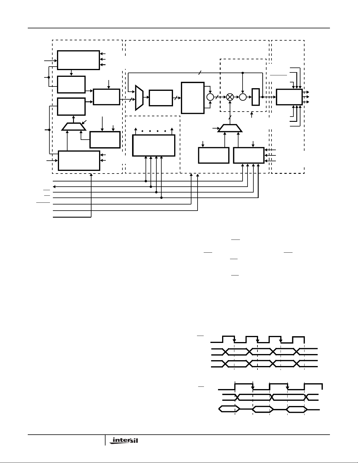
FIGURE 1. SERIAL FILTER BLOCK DIAGRAM
OUTPUT
FORMATTER
ACCUMULATOR
25
32
MUX
MULTIPLY/
+
DECIMATION
RATE
FIR SYM†
COEFFICIENT
RAM
R
E
G
†
MSB F/L†
FCLK†
CLKOUT
# BITS†
ROUND/
SATURATE
ROUND†
FORMAT†
GAIN COR†
RD EN†
FILTER LENGTH†
RAM ACCESS†
SYNCOUT
CLKOUT
DOUT
†Indicates configuration control word data parameter.
Functional Descriptions
The HSP43124 is a high performance digital filter designed to
process a serial input data stream. Asecondserial interfaceis
provided formixf actorinputs, which are multiplied by the input
samples as shown in Figure 1. The multiplier result is passed
to the Filter Compute Engine for processing.
The Filter Compute Engine centers around a single
multiply/accumulator (MAC). The MA C performs the sum-ofproducts required by a particular filter configuration. The
processing rate of the MAC is determined by the filter clock,
FCLK. Increasing FCLK relative to the input sample rate
increases the length of filter that can be realized.
The filtered results are passed to the Output Formatter where
they are rounded or truncated to a user defined bit width. The
Output Formatter then generates the timing and
synchronization signals required to serially transmit the data
to an external device.
Filter Configuration
The HSP43124 is configured for operation by loading a set of
eight control registers. These registers are written through a
bidirectional interface which is also used for reading the
control registers. The interface consists of an 8-bit data bus ,
C0-7, a 3-bit address bus, A0-2, and read/write lines, RD and
WR. The address map for the control registers is shown in
Table 1.
Data is written to the configuration control registers on the
falling edge of the
WR input. This requires that the address,
A0-2, and data, C0-7, be stable and valid on the falling edge
of the
WR, as shown in Figure 2.
active low when
RD is active low.
NOTE: WR should not be
Data is read from the configuration control registers on the
falling edge of the
RD input. The contents of a particular
register are accessed by setting up an address, A0-2, to the
falling edge of RD as shown in Figure 2. The data is output on
C0-7. The data on C0-7 remains valid until RD returns HIGH,
at which point the C0-7 bus is Three-Stated and functions as
an input. For proper operation, the address on A0-2 must be
held until RD returns “high” as shown in Figure 2.
NOTE: RD
should not be active low when WR is active low.
WRITE TIMING
WR
A0-2
C0-7
READ TIMING
RD
A0-2
C0-7
FIGURE 2. READ/WRITE TIMING
4

HSP43124
TABLE 1. CONFIGURATION CONTROL REGISTER FUNCTIONAL DESCRIPTION
BIT
ADDRESS REGISTER DESCRIPTION
000 Filter Configuration 2-0 Specifies thenumberof halfbands to use. Numberrangesfrom 0 to 5. Other
001 Programmable FIR Filter Length 7-0 Number of TapsintheProgrammable FIR Filter.For even or odd symmetric
010 Coefficient RAM Access 7-0 Coefficient RAM is loaded by multiple writes to this address. (See Writing
011 Input Format 4-0 Number of bits ininputdataword, from 8 (01000) to 24 (11000). Values out-
100 Output Timing 4-0 Number of FCLKS per CLKOUT. Range 1 to 32. (00000 = 32 FCLKS)
101 Output Format 4-0 Numberofbits in outputdata word, from8to 32.Avalue of32is represented
110 Filter Symmetry 1-0 00 = Even Symmetric FIR Coefficients
111 Mix Factor Format 4-0 Number of bits in mix factor, from 8 (01000) to 24 (11000). Values outside
POSITIONS BIT FUNCTION
values are invalid.
3 Filter Enable bit. 1 = Enable. 0 = Minimum filter bypass (either the FIR or
HBF must be enabled to get an output).
4 Coefficientreadenable. When setto1, enables readinganddisables writing
of coefficient RAM.
Coefficient RAM.
7-5 FIR Decimation Rate. Range is 1-8 (8 = 000).
filters, values range from 4- 256, 1 to 3 are invalid, and 0000000 = 256. For
asymmetric filters,thevalue loaded inthis register must betwo times the actual number of coefficients.
Coefficients section for additional details.)
side the range of 8 - 24 are invalid.
5 Number System. 0 = Two’s Complement, 1 = Offset Binary.
6 Serial Format. 1 = MSB First, 0 = LSB First.
7 Unused
5 1 = MSB First, 0 = LSB First.
6-7 Unused
by 00000, and values from 1 to 7 are invalid.
5 Round Select. 1 = Round to Selected Number of Bits, 0 = Truncate.
6 Number System. 0 = Two’s Complement, 1 = Offset Binary.
7 Gain Correction. 1 = Apply scale factor of 2 to data. 0 = No Scaling.
01 = Non-Symmetric Coefficients
10 = Odd Symmetric FIR
7-2 Reserved: Must be 0.
the range of 8 - 24 are invalid.
5 Serial Format. 1 = MSB First, 0 = LSB First.
6 Mix Factor Select. 1 = Serial Input, 0 = Weaver modulator look-up-table.
7 Unused
NOTE: This bit must be set to 0 prior to writing the
Writing Coefficients
The HSP43124 provides a register bank to store filter
coefficients for configurations which use the programmable
filter. The register bank consists of 128 thirty-two-bit
registers. Each register is loaded by 4 one byte writes to the
bidirectional interface used for loading the configuration
registers. The coefficients are loaded in order from least
significant byte (LSB) to most significant byte (MSB).
5
The coefficient registers are loaded by first setting the
coefficient read enable bit to “0” (bit 4 of the Filter
Configuration Register). Next, coefficients are loaded by
setting the A2-0 address to 010 (binary) and writing one byte
at a time as shown in Figure 3. The down loaded bytes are
stored in a holding register until the 4th write cycle. On
completion of the fourth write cycle, the contents of the
holding register are loaded into the Coefficient RAM, and the
write pointer is incremented to the next register. If the user
attempts to write more than 128 coefficients, the pointer

HSP43124
halts at the 128th register location, and writing is disabled.
The coefficient address pointer is reset when any other
configuration register is written or read.
NOTE: A new
coefficient set may be loaded during a filter calculation
at the risk of corrupting output data until the load is
complete.
WR
A0-2
C0-7
LSB MSB LSB MSB
FIRST COEFFICIENT SECOND COEFFICIENT
A0-2 = 010 (BINARY)
FIGURE 3. COEFFICIENT LOADING
The number of coefficients that must be loaded is dependent
on whether the coefficient set exhibits even symmetry, odd
symmetry, or asymmetry (see Figure 4).
EVEN SYMMETRIC
POINT
OF
SYMMETRY
ODD LENGTH
EVEN LENGTH
and ending with the center tap. The coefficient associated
with the first tap is the first to be multiplied by an incoming
data sample as shown in Figure 5. For even/odd symmetric
filters of length N, N/2 coefficients must be loaded if the filter
length is even,and (N+1)/2 coefficients must be loaded if the
filter length is odd. For example, a 17 tap symmetric filter
would require the loading of 9 coefficients. Enough storage
is provided for a 256 tap symmetric filter.
X
X(n) INPUT
FIRST
FILTER TAP
Y(n) = C0X2 + C1X1 + C2X
FIGURE 5. THREE TAP TRANSVERSAL FILTER
2
C0
ARCHITECTURE
X
1
-1
Z
C1 C2
+
0
X
0
-1
Z
LAST
FILTER TAP
Y(n) OUTPUT
For asymmetric filters the entire coefficient set must be
loaded. The coefficients are loaded in order starting with the
first tap and ending with the final filter tap (see Figure 5 for
tap/coefficient association). Enough storage is provided fora
128 tap asymmetric filter. For asymmetric filters the value
loaded into the Programmable Filter Length Register
addressed must be twice the actual number of coefficients.
NOTE: Filters with even symmetric coefficients exhibit symmetry about the center of the coefficient set. Most FIR filters have
coefficients which are symmetric in nature.
ODD SYMMETRIC
CENTER OF
COEFFICIENT SET
0.25
-0.1
0.1
0.5
-0.25
-0.5
NOTE: Odd symmetric coefficients have a coefficient envelope
which has the characteristics of an odd function (i.e. coefficients which are equidistant from the center of the coefficient
set are equal in magnitude but opposite in sign). Coefficients
designed to function as a differentiator or Hilbert Transform exhibit these characteristics.
ASYMMETRIC
NOTE: Asymmetric Coefficient sets exhibit no symmetry.
FIGURE 4. COEFFICIENT CHARACTERISTICS
For filters that exhibit either even or odd symmetry, only the
unique half of the coefficient set must be loaded. The
coefficients are loaded in order starting with the first filter tap
Reading Coefficients
The coefficients are read from the storage registers one byte
at a time via C0-7 as shown in Figure 6. To read the
coefficients, the user first sets the Coefficient Read Enable
bit to 1 (bit 4 of Filter Configuration Control Register). Setting
this bit resets the RAM read pointer and disables the RAM
from being written. Next, with A2-0 = 010, multiple “high” to
“low” transitions of
byte at a time, in the order they were written.
should not be “low” when
RD
A0-2
C0-7
LSB
RD, output the coefficients on C0-7, one
NOTE: RD
WR is “low”
A0-2 = 010 (BINARY)
MSB LSB
FIRST COEFFICIENT SECOND COEFFICIENT
FIGURE 6. COEFFICIENT READING
.
MSB
Data Input
Data is serially input to the HSP43124 through the DIN input.
On the rising edge of SCLK, the bit value present at DIN is
clocked into the Variable Length Shift Register. The
beginning of a serial data word is designated by asserting
SYNCIN “high” one SCLK prior to the first data bit as shown
6
 Loading...