

Intersil Corporation HS-82C85RH Datasheet
August 1995
HS-82C85RH
Radiation Hardened
CMOS Static Clock Controller/Generator
Features
• Radiation Hardened
- Total Dose > 10
- Transient Upset > 10
- Latch Up Free EPI-CMOS
• Very Low Power Consumption
• Pin Compatible with NMOS 8285 and Intersil 82C85
• Generates System Clocks for Microprocessors and Peripherals
• Complete Control Over System Clock Operation for Very Low
System Power
- Stop-Oscillator
- Stop-Clock
- Low Frequency (Slo) Mode
- Full Speed Operation
• DC to 15MHz Operation (DC to 5MHz System Clock)
• Generates Both 50% and 33% Duty Cycle Clocks (Synchronized)
• Uses Either Parallel Mode Crystal Circuit or External Frequency
Source
• Hardened Field, Self-Aligned, Junction Isolated CMOS Process
• Single 5V Supply
• Military Temperature Range -55
5
RAD (Si)
8
RAD (Si)/s
o
C to +125oC
Description
The Intersil HS-82C85RH is a high performance, radiation hardened
CMOS Clock Controller/Generator designed to support systems utilizing
radiation hardened static CMOS microprocessors such as the
HS-80C86RH. The HS-82C85RH contains a crystal controlled oscillator,
reset pulse conditioning, halt/restart logic, and divide-by-256 circuitry.
These features provide the means to stop the system clock, stop the clock
oscillator, or run the system at a low frequency (CLK/256), enhancing
control of static system power dissipation and allowing system shut-down
during periods of external stress.
Static CMOS circuit design insures low operating power and permits
operation with an external frequency source from DC to 15MHz. Crystal
controlled operation to 15MHz is guaranteed with the use of a parallel,
fundamental mode crystal and two small load capacitors. Outputs are
guaranteed compatible with both CMOS and TTL specifications. The Intersil hardened field CMOS process results in performance equal to or
greater than existing radiation resistant products at a fraction of the power.
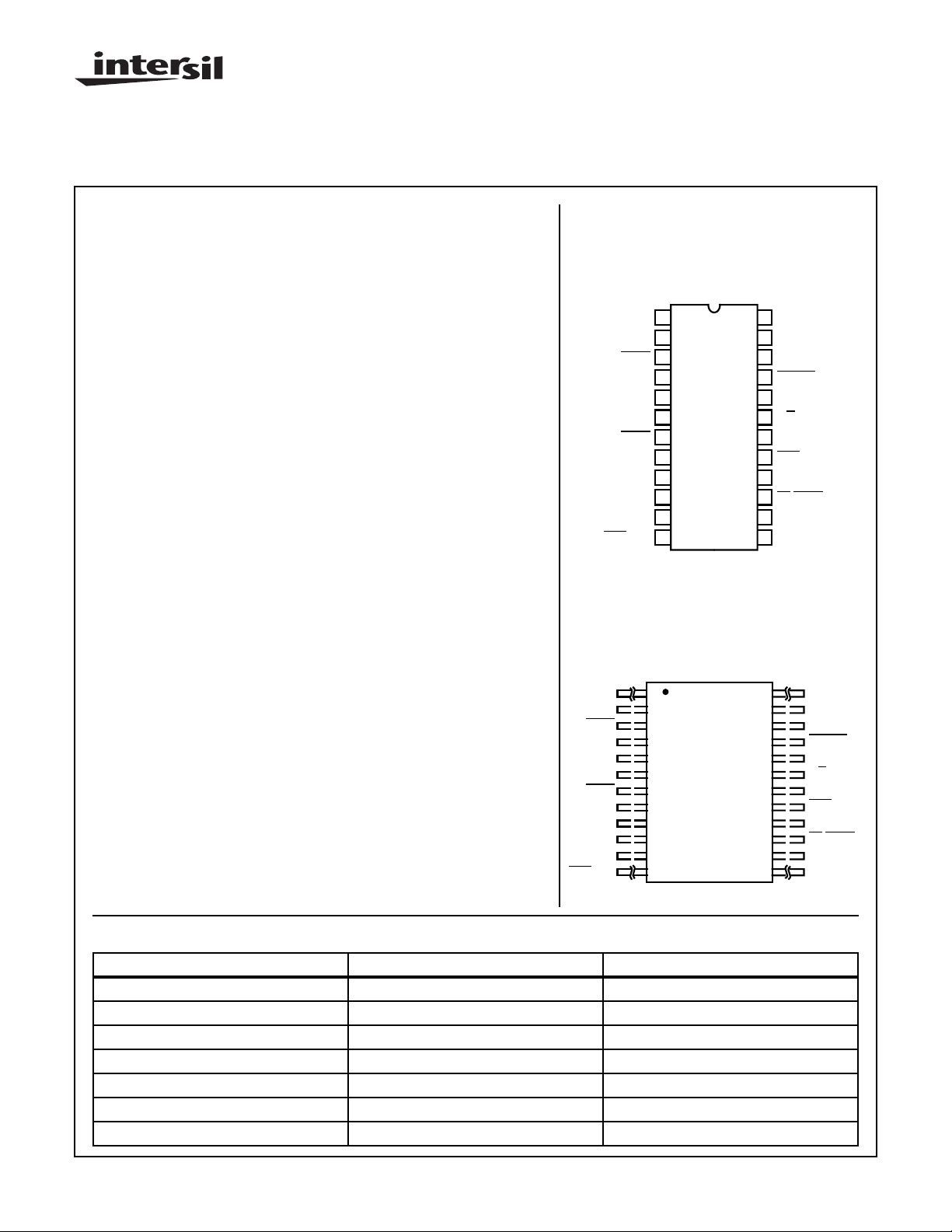
Pinouts
24 LEAD CERAMIC DUAL-IN-LINE
METAL SEAL PACKAGE (SBDIP)
MIL-STD-1835 CDIP2-T24
TOP VIEW
CSYNC
READY
SLO/FST
FLATPACK PACKAGE (FLATPACK)
CSYNC
PCLK
AEN1
RDY1
READY
RDY2
AEN2
CLK
GND
CLK50
START
SLO/FST
1
2
PCLK
3
AEN1
RDY1
4
5
6
RDY2
7
AEN2
8
CLK
9
GND
10
CLK50
11
START
12
24 LEAD CERAMIC METAL SEAL
MIL-STD-1835 CDFP4-F24
TOP VIEW
1
2
3
4
5
6
7
8
9
10
11
12
24
23
22
21
20
19
18
17
16
15
14
13
24
23
22
21
20
19
18
17
16
15
14
13
VDD
X1
X2
ASYNC
EFI
F/C
OSC
RES
RESET
S2/STOP
S1
S0
VDD
X1
X2
ASYNC
EFI
F/
OSC
RES
RESET
S2/STOP
S1
S0
C
Ordering Information
PART NUMBER TEMPERATURE RANGE PACKAGE
HS1-82C85RH-Q -55oC to +125oC 24 Lead SBDIP
HS1-82C85RH-8 -55oC to +125oC 24 Lead SBDIP
HS1-82C85RH/Sample +25oC 24 Lead SBDIP
HS9-82C85RH/Proto -55oC to +125oC 24 Lead Ceramic Flatpack
HS9-82C85RH-Q -55oC to +125oC 24 Lead Ceramic Flatpack
HS9-82C85RH-8 -55oC to +125oC 24 Lead Ceramic Flatpack
HS9-82C85RH/Sample +25oC 24 Lead Ceramic Flatpack
CAUTION: These devices are sensitive to electrostatic discharge; follow proper IC Handling Procedures.
http://www.intersil.com or 407-727-9207
| Copyright © Intersil Corporation 1999
992
Spec Number
518061
File Number 3044.1
DB NA

HS-82C85RH
Pin Description
PIN
PIN
X1
X2
EFI 20 I EXTERNAL FREQUENCY IN: When F/C is HIGH, CLK is generated from the EFI input signal.
F/C 19 I FREQUENCY/CRYSTAL SELECT: F/C selects either the crystal oscillator or the EFI input as the
START 11 I A low-to-high transition on START will restart the CLK, CLK50 and PCLK outputs after the
S0
S1
S2/STOP
SLO/FST 12 I SLO/FST is a level-triggered input. When HIGH, the CLK and CLK50 outputs run at the maximum
CLK 8 O PROCESSOR CLOCK: CLK is the clock output used by the HS-80C86RH processor and other
CLK50 10 O 50% DUTY CYCLE CLOCK: CLK50 is an auxiliary clock with a 50% duty cycle and is synchro-
PCLK 2 O PERIPHERAL CLOCK: PCLK is a peripheral clock signal whose output frequency is equal to the
OSC 18 O OSCILLATOR OUTPUT: OSC is the output of the internal oscillator circuitry. Its frequency is
NUMBER TYPE DESCRIPTION
23
22
13
14
15
I
CRYSTAL CONNECTIONS: X1 and X2 are the crystal oscillator connections. The crystal
O
frequency must be three times the maximum desired processor clock frequency. X1 is the
oscillator circuit input and X2 is the output of the oscillator circuit.
This input signal should be a square wave with a frequency of three times the maximum desired
CLK output frequency.
main frequency source. When F/C is LOW, the HS-82C85RH clocks are derived from the crystal
oscillator circuit. When F/C is HIGH, CLK is generated from the EFI input. F/C cannot be dynamically switched during normal operation.
appropriate restart sequence is completed.
When in the crystal mode (F/C LOW) with the oscillator stopped, the oscillator will be restarted
when a Start command is received. The CLK, CLK50 and PCLK outputs will start after the oscillator input signal (X1) reaches the Schmitt trigger input threshold and an 8K internal counter
reaches terminal count. If F/C is HIGH (EFI mode), CLK, CLK50 and PCLK will restart within 3 EFI
cycles after START is recognized.
The HS-82C85RH will restart in the same mode (SLO/FST) in which it stopped. A high level on
START disables the STOP mode.
I
S2/STOP, S1, S0 are used to stop the HS-82C85RH clock outputs (CLK, CLK50, PCLK) and are
I
sampled by the rising edge of CLK. CLK, CLK50 and PCLK are stopped byS2/STOP,S1, S0 being
I
in the LHH state on the low-to-high transition of CLK. This LHH state must follow a passive HHH
state occurring on the previous low-to-high CLK transition. CLK and CLK50 stop in the high state.
PCLK stops in it’s current state (high or low).
When in the crystal mode (F/C) low and a STOP command is issued, the HS-82C85RH oscillator
will stop along with the CLK, CLK50 and PCLK outputs. When in the EFI mode, only the CLK,
CLK50 and PCLK outputs will be halted. The oscillator circuit if operational, will continue to run.
The oscillator and/or clock is restarted by the START input signal going true (HIGH) or the reset
input (RES) going low.
frequency (crystal or EFI frequency divided by 3). When LOW, CLK and CLK50 frequencies are
equal to the crystal or EFI frequency divided by 768. SLO/FST mode changes are internally
synchronized to eliminate glitches on the CLK and CLK50. START and STOP control of the
oscillator or EFI is available in either the SLOW or FAST frequency modes.
The SLO/FST input must be held LOW for at least 195 OSC/EFI clock cycles before it will be
recognized. This eliminates unwanted frequency changes which could be caused by glitches or
noise transients. The SLO/FST input must be held HIGH for at least 6 OSC/EFI clock pulses to
guarantee a transition to FAST mode operation.
peripheral devices. When SLO/FST is high, CLK has an output frequency which is equal to the
crystal or EFI input frequency divided by three. When SLO/FST is low, CLK has an output frequency which is equal to the crystal or EFI input frequency divide by 768. CLK has a 33% duty cycle.
nized to the falling edge of CLK. When SLO/FST is high, CLK50 has an output frequency which
is equal to the crystal or EFI input frequency divided by 3. When SLO/FST is low, CLK50 has an
output frequency equal to the crystal or EFI input frequency divided by 768.
crystal or EFI input frequency divided by six and has a 50% duty cycle. PCLK frequency is
unaffected by the state of the SLO/FST input.
equal to that of the crystal oscillator circuit. OSC is unaffected by the state of the SLO/FST input.
When the HS-82C85RH is in the crystal mode (F/C LOW) and a STOP command is issued, the
OSC output will stop in the HIGH state. When the HS-82C85RH is in the EFI mode (F/C HIGH),
the oscillator (if operational) will continue to run when a STOP command is issued and OSC
remains active.
993
Spec Number 518061
HS-82C85RH
Pin Description
(Continued)
PIN
PIN
NUMBER TYPE DESCRIPTION
RES 17 I RESET IN: RES is an active LOW signal which is used to generate RESET. The HS-82C85RH
provides a Schmitt trigger input so that an RC connection can be used to establish the power-up
reset of proper duration. RES starts crystal oscillator operation.
RESET 16 O RESET: RESET is an active HIGH signal which is used to reset the HS-80C86RH processor. Its
timing characteristics are determined by RES. RESET is guaranteed to be HIGH for a minimum
of 16 CLK pulses after the rising edge of RES.
CSYNC 1 I CLOCK SYNCHRONIZATION: CSYNC is an active HIGH signal which allows multiple HS-
82C85RHs to be synchronized to provide multiple in-phase clock signals. When CSYNC is HIGH,
the internal counters are reset and force CLK, CLK50 and PCLK into a HIGH state. When CSYNC
is LOW, the internal counters are allowed to count and the CLK,CLK50 and PCLK outputs are
active. CSYNC must be externally synchronized to EFI.
AEN1
AEN2
3
7
I
ADDRESS ENABLE: AEN is an active LOW signal. AEN serves to qualify its respective Bus
I
Ready Signal (RDY1 or RDY2). AEN1 validates RDY1 while AEN2 validates RDY2. Two AEN
signal inputs are useful in system configurations which permit the processor to access two MultiMaster System Buses.
RDY1
RDY2
4
6
I
BUS READY: (Transfer Complete). RDY is an active HIGH signal which is an indication from a
I
device located on the system data bus that data has been received, or is available. RDY1 is
qualified by AEN1 while RDY2 is qualified by AEN2.
ASYNC 21 I READY SYNCHRONIZATION SELECT: ASYNC is an input which defines the synchronization
mode of the READY logic. When ASYNC is LOW, two stages of READY synchronization are provided. When ASYNC is left open or HIGH a single stage of READY synchronization is provided.
READY 5 O READY: READY is an active HIGH signal which is used to inform the HS-80C86RH that it may
conclude a pending data transfer.
GND 9 I Ground
VDD 24 I +5V power supply
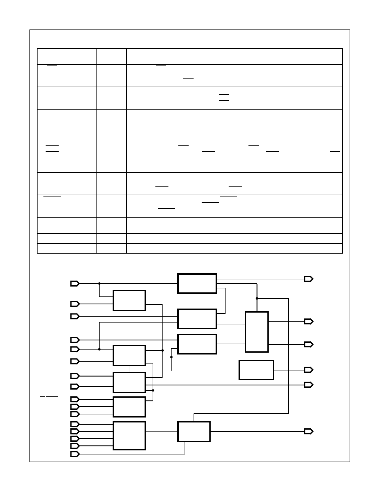
Functional Diagram
RES (17)
START (11)
CSYNC (1)
SLO/FST (12)
C (19)
F/
EFI (20)
X2 (22)
X1 (23)
S2/STOP (15)
S1 (14)
SO (13)
RDY1 (4)
AEN1 (3)
AEN2 (7)
RDY2 (6)
ASYNC (21)
RESTART
LOGIC
EXTERNAL
FREQUENCY
SELECT
OSC
OSCILLATOR
STOP
LOGIC
READY
SELECT
RESTART
HALT
RESET PULSE
CONDITIONING
LOGIC
SYNC
LOGIC
SPEED SELECT
÷ 256 OR ÷ 1
SELECTED OSC
READY
SYNC
SYNC
MASTER
OSC
CLOCK
LOGIC
(÷ 3)
PERIPHERAL
CLOCK
(
÷ 6)
(24) VDD
(9) GND
(16) RESET
(8) CLK
(10) CLK50
(2) PCLK
(18) OSC
(5) READY
994
Spec Number 518061

Specifications HS-82C85RH
Absolute Maximum Ratings Reliability Information
Supply Voltage . . . . . . . . . . . . . . . . . . . . . . . . . . . . . . . . . . . . .+6.5V
Input, Output or I/O Voltage . . . . . . . . . . . . .VSS-0.3V to VDD+0.3V
Storage Temperature Range . . . . . . . . . . . . . . . . . -65oC to +150oC
Junction Temperature. . . . . . . . . . . . . . . . . . . . . . . . . . . . . . +175oC
Lead Temperature (Soldering 10s). . . . . . . . . . . . . . . . . . . . +300oC
Typical Derating Factor. . . . . . . . . .5.33mA/MHz Increase in IDDOP
ESD Classification . . . . . . . . . . . . . . . . . . . . . . . . . . . . . . . . Class 1
CAUTION: Stresses above those listed in “Absolute Maximum Ratings” may cause permanent damage to the device. This is a stress only rating and operation
of the device at these or any other conditions above those indicated in the operational sections of this specification is not implied.
Operating Conditions
Operating Voltage Range. . . . . . . . . . . . . . . . . . . . . +4.5V to +5.5V
Operating Temperature Range. . . . . . . . . . . . . . . . -55oC to +125oC
RESET Input High Voltage. . . . . . . . . . . . . . . . . . . . . . 3.5V to VDD
TABLE 1. DC ELECTRICAL PERFORMANCE CHARACTERISTICS
PARAMETER SYMBOL CONDITIONS
Thermal Resistance θ
SBDIP Package. . . . . . . . . . . . . . . . . . . . 52oC/W 12oC/W
Ceramic Flatpack Package . . . . . . . . . . . 70oC/W 10oC/W
Maximum Package Power Dissipation at +125oC Ambient
SBDIP Package. . . . . . . . . . . . . . . . . . . . . . . . . . . . . . . . . .0.96W
Ceramic Flatpack Package . . . . . . . . . . . . . . . . . . . . . . . . . 0.71W
If device power exceeds package dissipation capability, provide heat
sinking or derate linearly at the following rate:
SBDIP Package. . . . . . . . . . . . . . . . . . . . . . . . . . . . . . .19.2mW/C
Ceramic Flatpack Package . . . . . . . . . . . . . . . . . . . . . .14.3mW/C
Input Low Voltage . . . . . . . . . . . . . . . . . . . . . . . . . . . . . .0V to +0.8V
Input High Voltage. . . . . . . . . . . . . . . . . . . . . . . . . . . . . 3.5V to VDD
GROUP A
SUBGROUP TEMPERATURE
JA
LIMITS
θ
JC
UNITSMIN MAX
CLK or CLK50 Output
High Voltage
Output High Voltage VOH VDD = 4.5V, IO = -2.5mA,
Output Low Voltage VOL VDD = 4.5V, IO = 5.0mA,
Input Leakage Current
Bus Hold High Leakage Current (Note 1)
Standby Power Supply Current
Operating Power
Supply Current
Functional Tests FT VDD = 4.5V and 5.5V,
Noise Immunity
Functional Test
VOH VDD = 4.5V, IO = -5.0mA,
VIN = 0V or 4.5V
VIN = 0V or 4.5V
VIN = 0V or 4.5V
IIL or IIH VDD = 5.5V, VIN = 0V or
5.5V, Input Pins except: 11 to
15, 21, 23
IBHH VDD = 4.5V, 5.5V, VIN =
3.0V, Pins: 11 to 15, 21
IDDSB VDD = 5.5V, VIN = GND or
VDD, IO = 0mA
IDDOP VDD = 5.5V, VIN = GND or
VDD, IO = 0mA, Crystal
Frequency = 15MHz
VIN = GND or VDD, f = 1MHz
FN VDD = 5.5V,
VIN = GND or 3.5V and
VDD = 4.5V,
VIN = 0.8V or VDD
1, 2, 3 -55oC, +25oC,
+125oC
1, 2, 3 -55oC, +25oC,
+125oC
1, 2, 3 -55oC, +25oC,
+125oC
1, 2, 3 -55oC, +25oC,
+125oC
1, 2, 3 -55oC, +25oC,
+125oC
1, 2, 3 -55oC, +25oC,
+125oC
1, 2, 3 -55oC, +25oC,
+125oC
7, 8A, 8B -55oC, +25oC,
+125oC
7, 8A, 8B -55oC, +25oC,
+125oC
VDD
-0.4
VDD
-0.4
- 0.4 V
-1.0 1.0 µA
-200 -20 µA
- 100 µA
-80mA
-- -
-- -
-V
-V
NOTE:
1. IBHH should be measured after raising VIN to VDD and then lowering to 3.0V
995
Spec Number 518061

Specifications HS-82C85RH
TABLE 2. AC ELECTRICAL PERFORMANCE CHARACTERISTICS VDD = 4.5V, TA = -55oC to +125oC
GROUP A
PARAMETER SYMBOL CONDITIONS
TIMING REQUIREMENTS
External Frequency High
Time
External Frequency Low
Time
EFI or Crystal Period TELEL 9, 10, 11 -55oC, +25oC, +125oC65 -ns
External Frequency Input
Duty Cycle
Crystal Frequency FX 9, 10, 11 -55oC, +25oC, +125oC 2.4 15 MHz
RDY1, RDY2 Active Setup
to CLK
RDY1, RDY2 Active Setup
to CLK
RDY1, RDY2 Inactive Setup
to CLK
RDY1, RDY2 Hold to CLK TCLR1X 9, 10, 11 -55oC, +25oC, +125oC0 -ns
ASYNC Setup to CLK TAYVCL 9, 10, 11 -55oC, +25oC, +125oC84 -ns
ASYNC Hold to CLK TCLAYX 9, 10, 11 -55oC, +25oC, +125oC0 -ns
AEN1, AEN2 Setup to
RDY1, RDY2
AEN1, AEN2 Hold to CLK TCLA1X 9, 10, 11 -55oC, +25oC, +125oC0 -ns
CSYNC Setup to EFI TYHEH 9, 10, 11 -55oC, +25oC, +125oC17 -ns
CSYNC Hold to EFI TEHYL 9, 10, 11 -55oC, +25oC, +125oC17 -ns
CSYNC Pulse Width TYHYL 9, 10, 11 -55oC, +25oC, +125oC 2TELEL - ns
RES Setup to CLK TI1HCL Note 3 9, 10, 11 -55oC, +25oC, +125oC 105 - ns
S0, S1, S2/STOP Setup to
CLK
S0, S1, S2/STOP Hold to
CLK
RES, START Setup to CLK TRSVCH Note 3 9, 10, 11 -55oC, +25oC, +125oC 105 - ns
RES (Low) or START (High)
Pulse Width
SLO/FST Setup to PCLK TSFPC Note 3 9, 10, 11 -55oC, +25oC, +125oC TEHEL+170 - ns
TIMING RESPONSES
CLK/CLK50 Cycle Period TCLCL 9, 10, 11 -55oC, +25oC, +125oC 200 - ns
CLK HIGH Time TCHCL 9, 10, 11 -55oC, +25oC, +125oC (1/3 TCLCL)+3-ns
TEHEL 90% - 90%
VIN
TELEH 10% - 10%
VIN
TEFIDC 9, 10, 11 -55oC, +25oC, +125oC45 55%
TR1VCL ASYNC =
High
TR1VCH ASYNC = Low 9, 10, 11 -55oC, +25oC, +125oC55 -ns
TR1VCL 9, 10, 11 -55oC, +25oC, +125oC55 -ns
TA1VR1V 9, 10, 11 -55oC, +25oC, +125oC25 -ns
TSVCH 9, 10, 11 -55oC, +25oC, +125oC55 -ns
TCHSX 9, 10, 11 -55oC, +25oC, +125oC55 -ns
TSHSL 9, 10, 11 -55oC, +25oC, +125oC 2/3 TCLCL - ns
SUBGROUP TEMPERATURE
9, 10, 11 -55oC, +25oC, +125oC25 -ns
9, 10, 11 -55oC, +25oC, +125oC25 -ns
9, 10, 11 -55oC, +25oC, +125oC55 -ns
LIMITS
UNITSMIN MAX
CLK LOW TCLCH 9, 10, 11 -55oC, +25oC, +125oC (2/3 TCLCL)
-15
CLK50 HIGH Time T5CHCL 9, 10, 11 -55oC, +25oC, +125oC (1/2 TCLCL)
-7.5
CLK50 LOW Time T5CLCH 9, 10, 11 -55oC, +25oC, +125oC (1/2 TCLCL)
-7.5
PCLK HIGH Time TPHPL 9, 10, 11 -55oC, +25oC, +125oC TCLCL-20 - ns
-ns
-ns
-ns
Spec Number 518061
996

Specifications HS-82C85RH
TABLE 2. AC ELECTRICAL PERFORMANCE CHARACTERISTICS VDD = 4.5V, TA = -55oC to +125oC (Continued)
GROUP A
PARAMETER SYMBOL CONDITIONS
PCLK LOW Time TPLPH 9, 10, 11 -55oC, +25oC, +125oC TCLCL-20 - ns
Ready Inactive to CLK TRYLCL Note 4 9, 10, 11 -55oC, +25oC, +125oC-8 -ns
Ready Active to CLK TRYHCH Note 3 9, 10, 11 -55oC, +25oC, +125oC 2/3(TCLCL)
CLK to Reset Delay TCLIL 9, 10, 11 -55oC, +25oC, +125oC - 65 ns
CLK to PCLK HIGH Delay TCLPH 9, 10, 11 -55oC, +25oC, +125oC - 40 ns
CLK to PCLK LOW Delay TCLPL 9, 10, 11 -55oC, +25oC, +125oC - 40 ns
OSC to CLK HIGH Delay TOHCH 9, 10, 11 -55oC, +25oC, +125oC-5 60ns
OSC to CLK LOW Delay TOHCL 9, 10, 11 -55oC, +25oC, +125oC 2 70 ns
OSC LOW to CLK50 HIGH
Delay
CLK LOW to CLK50 LOW
Skew
NOTES:
1. ACs tested at worst case VDD, guaranteed over full operating range
2. Setup and hold necessary only to guarantee recognition at next clock
3. Applies only to T3, TW states
4. Applies only to T2 states
5. All timing delays are measured at 1.5V, unless otherwise noted
6. Timing measurements made with EFI duty cycle = 50%
TOLCH 9, 10, 11 -55oC, +25oC, +125oC-5 60ns
TCLC50L 9, 10, 11 -55oC, +25oC, +125oC - 10 ns
SUBGROUP TEMPERATURE
LIMITS
UNITSMIN MAX
-ns
-15
TABLE 3. ELECTRICAL PERFORMANCE CHARACTERISTICS
LIMITS
PARAMETER SYMBOL CONDITION TEMPERATURE
Input Capacitance CIN VDD = Open, f = 1MHz, Note 2 TA = +25oC-5pF
Output Capacitance COUT VDD = Open, f = 1MHz, Note 2 TA = +25oC - 15 pF
RESET Input
Hysteresis
TIMING REQUIREMENTS
RES or START Valid
to CLK Low
STOP Command
Valid to CLK High
TIMING RESPONSES
CLK/CLK50 Rise
Time
CLK/CLK50 Fall Time TCL1CL2 VDD = 4.5V and 5.5V, 3.5V to
Output Rise Time
(Except CLK)
Output Fall Time
(Except CLK)
(+)VT - (-)VT VDD = 4.5V and 5.5V -55oC < TA < +125oC 0.25 - V
TSTART VDD = 4.5V and 5.5V -55oC < TA < +125oC 2TELEL
+3
TSTOP VDD = 4.5V and 5.5V -55oC < TA < +125oC TCLCL +
TCLCH
TCH1CH2 VDD = 4.5V and 5.5V, 1.0V to
3.5V
1.0V
TOLOH VDD = 4.5V and 5.5V, 0.8V to
2.0V
TOHOL VDD = 4.5V and 5.5V, 2.0V to
0.8V
-55oC < TA < +125oC - 15 ns
-55oC < TA < +125oC - 15 ns
-55oC < TA < +125oC - 25 ns
-55oC < TA < +125oC - 25 ns
-ns
3TCHCH
+55
UNITSMIN MAX
ns
997
Spec Number 518061

Specifications HS-82C85RH
TABLE 3. ELECTRICAL PERFORMANCE CHARACTERISTICS
PARAMETER SYMBOL CONDITION TEMPERATURE
LIMITS
UNITSMIN MAX
Start/Reset Valid to
CLK Low
RESET Output Time
High
NOTES:
1. The parameters listed in table 3 are controlled via design or process parameters and are not directly tested. These parameters are
characterized upon initial design release and upon design changes which would affect these characteristics.
2. All measurements referenced to device ground.
3. Oscillator start-up time depends on several factors including crystal frequency, crystal manufacturer, capacitive load, temperature, power
supply voltage, etc. This parameter is given for information only.
See +25oC limits in Table 1 and Table 2 for Post RAD limits (Subgroups 1, 7, 9)
TOST VDD = 4.5V and 5.5V (TYP)
Note 3
TRST VDD = 4.5V and 5.5V -55oC < TA < +125oC16
TABLE 4. POST 100K RAD ELECTRICAL PERFORMANCE CHARACTERISTICS
TABLE 5. BURN-IN DELTA PARAMETERS (+25oC)
PARAMETER SYMBOL DELTA LIMITS
Static Current IDDSB ±20µA
Input Leakage Current IIL, IIH ±200nA
Low Level Output Voltage VOL ±80mV
High Level Output Voltage VOH ±150mV
-55oC < TA < +125oC- 3 ms
(TCLCL)
-ms
TABLE 6. APPLICABLE SUBGROUPS
GROUP A SUBGROUPS
CONFORMANCE
GROUP
Initial Test 100% 5004 1, 7, 9 1 (Note 2) 1, 7, 9
Interim Test 100% 5004 1, 7, 9, ∆ 1, ∆ (Note 2) 1, 7, 9
PDA 100% 5004 1, 7, ∆ - 1, 7
Final Test 100% 5004 2, 3, 8A, 8B, 10, 11 - 2, 3, 8A, 8B, 10, 11
Group A (Note 1) Sample 5005 1, 2, 3, 7, 8A, 8B, 9, 10, 11 - 1, 2, 3, 7, 8A, 8B, 9,
Subgroup B5 Sample 5005 1, 2, 3, 7, 8A, 8B, 9, 10, 11, ∆ 1, 2, 3, ∆ (Note 2) N/A
Subgroup B6 Sample 5005 1, 7, 9 - N/A
Group C Sample 5005 N/A N/A 1, 2, 3, 7, 8A, 8B, 9,
Group D Sample 5005 1, 7, 9 - 1, 7, 9
Group E, Subgroup 2 Sample 5005 1, 7, 9 - 1, 7, 9
NOTES:
1. Alternate Group A testing in accordance with MIL-STD-883 method 5005 may be exercised.
2. Table 5 parameters only
MIL-STD-883
METHOD
TESTED FOR -Q
RECORDED
FOR -Q TESTED FOR -8
10, 11
10, 11
RECORDED
FOR -8
998
Spec Number 518061
 Loading...