

Intersil Corporation HS-82C55ARH Datasheet

September 1995
HS-82C55ARH
Radiation Hardened
CMOS Programmable Peripheral Interface
Features
• Radiation Hardened
- Total Dose >10
- Transient Upset <10
- Latch Up Free EPI-CMOS
• Low Power Consumption
- IDDSB = 20µA
• Pin Compatible with NMOS 8255A and the Intersil 82C55A
• High Speed, No “Wait State” Operation with 5MHz HS-80C86RH
• 24 Programmable I/O Pins
• Bus-Hold Circuitry on All I/O Ports Eliminates Pull-Up Resistors
• Direct Bit Set/Reset Capability
• Enhanced Control Word Read Capability
• Hardened Field, Self-Aligned, Junction Isolated CMOS Process
• Single 5V Supply
• 2.0mA Drive Capability on All I/O Port Outputs
• Military Temperature Range: -55
5
RAD (Si)
8
RAD (Si)/s
o
C to +125oC
Description
The Intersil HS-82C55ARH is a high performance, radiation hardened
CMOS version of the industry standard 8255A and is manufactured using a
hardened field, self-aligned silicongate CMOS process. It is a general
purpose programmable I/O device which may be used with many different
microprocessors. There are 24 I/O pins which are organized into two 8-bit
and two 4-bit ports. Each port may be programmed to function as either an
input or an output. Additionally, one of the 8-bit ports may be programmed
for bi-directional operation,and the two 4-bit ports can be programmed to
provide handshaking capabilities. The high performance, radiation
hardness, and industry standard configuration of the HS-82C55ARH make
it compatible with the HS-80C86RH radiation hardened microprocessor.
Static CMOS circuit design insures low operating power. Bus hold circuitry
eliminates the need for pull-up resistors. The Intersil hardened field CMOS
process results in performance equal to or greater than existing radiation
resistant products at a fraction of the power.
Pinout
40 LEAD CERAMIC DUAL-IN-LINE
METAL SEAL PACKAGE (SBDIP)
MIL-STD-1835 CDIP2-T40
TOP VIEW
1
PA3
PA2
PA1
PA0
RD
CS
GND
A1
A0
PC7
PC6
PC5
PC4
PC0
PC1
PC2
PC3
PB0
PB1
PB2
2
3
4
5
6
7
8
9
10
11
12
13
14
15
16
17
18
19
20
40
39
38
37
36
35
34
33
32
31
30
29
28
27
26
25
24
23
22
21
PA4
PA5
PA6
PA7
WR
RESET
D0
D1
D2
D3
D4
D5
D6
D7
VDD
PB7
PB6
PB5
PB4
PB3
Pin Description
PIN DESCRIPTION
D7 - D0 Data Bus (Bi-Directional
RESET Reset Input
CS Chip Select
RD Read Input
WR Write Input
Ordering Information
PART NUMBER TEMPERATURE PACKAGE
HS1-82C55ARH-Q -55oC to +125oC 40 Lead SBDIP
HS1-82C55ARH-8 -55oC to +125oC 40 Lead SBDIP
HS1-82C55ARH/Sample +25oC 40 Lead SBDIP
CAUTION: These devices are sensitive to electrostatic discharge; follow proper IC Handling Procedures.
http://www.intersil.com or 407-727-9207
| Copyright © Intersil Corporation 1999
970
A0 - A1 Port Address
PA7 - PA0 Port A (Bit)
PB& - PB0 Port B (Bit)
PC7 - PC0 Port C (Bit)
VDD +5 volts
GND 0 volts
Spec Number
File Number 3191.1
DB NA
518060

HS-82C55ARH
Pin Description
PIN
SYMBOL
PA0-7 1-4, 37-40 I/O Port A: General purpose I/O Port. Data direction and mode is determined by the contents
PB0-7 18-25 I/O Port B: General purpose I/O port. See Port A.
PC0-3 14-17 I/O Port C (Lower): Combination I/O port and control port associated with Port B. See Port A.
PC4-7 10-13 I/O Port C (Upper): Combination I/O Port and control port associated with Port A. See Port A.
D0-7 27-34 I/O Bidirectional Data Bus: Three-State data bus enabled as an input when CS and WR are
VDD 26 I VDD: The +5V power supply pin. A 0.1µF capacitor between pins 26 and 7 is recommend-
GND 7 I Ground.
CS 6 I Chip Select: A “low” on this input pin enables the communication between the
RD 5 I Read: A “low” on this input pin enables the HS-82C55ARH to send the data or status
WR 36 I Write: A “low” on this input pin enables the CPU to write data or control words into the
A0 and A1 8, 9 I Port Select 0 and Port Select 1: These input signals, in conjunction with the RD and WR
Reset 35 I Reset: A “high” on this input clears the control register and all ports (A, B, C) are set to the
NUMBERS TYPE DESCRIPTION
of the Control Word.
low and as an output when CS and RD are low.
ed for decoupling.
HS-82C55ARH and the CPU.
information to the CPU on the data bus. In essence, it allows the CPU to “read from” the
HS-82C55ARH.
HS-82C55ARH.
inputs, control the selection of one of the three ports or the control word registers. They are
normally connected to the Least Significant Bits of the address bus (A0 and A1).
input mode. “Bus hold” devices internal to the HS-82C55ARH will hold the I/O port inputs
to a logic “1” state with a maximum hold current of 400µA.
Functional Diagram
POWER
SUPPLIES
BIDIRECTIONAL
DATA BUS
D7 - D0
RD
WR
A1
A0
RESET
READ/WRITE
DATA
BUS
BUFFER
CONTROL
LOGIC
+5V
GND
GROUP A
CONTROL
8-BIT INTERNAL
GROUP B
CONTROL
DATA BUS
GROUP A
PORT A
(8)
GROUP A
PORT C
UPPER (4)
GROUP B
PORT C
LOWER (4)
GROUP B
PORT B
(8)
I/O
PA7 - PA0
I/O
PC7 - PC4
I/O
PC3 - PC0
I/O
PB7 - PB0
CS
Spec Number 518060
971
Specifications HS-82C55ARH
Absolute Maximum Ratings Reliability Information
Supply Voltage . . . . . . . . . . . . . . . . . . . . . . . . . . . . . . . . . . . . .+7.0V
Input, Output or I/O Voltage . . . . . . . . . . . . .VSS-0.3V to VDD+0.3V
Storage Temperature Range . . . . . . . . . . . . . . . . . -65oC to +150oC
Junction Temperature. . . . . . . . . . . . . . . . . . . . . . . . . . . . . . +175oC
Lead Temperature (Soldering 10s). . . . . . . . . . . . . . . . . . . . +300oC
ESD Classification . . . . . . . . . . . . . . . . . . . . . . . . . . . . . . . . Class 1
CAUTION: Stresses above those listed in “Absolute Maximum Ratings” may cause permanent damage to the device. This is a stress only rating and operation
of the device at these or any other conditions above those indicated in the operational sections of this specification is not implied.
Operating Conditions
Operating Voltage Range. . . . . . . . . . . . . . . . . . . . . +4.5V to +5.5V
Operating Temperature Range. . . . . . . . . . . . . . . . -55oC to +125oC
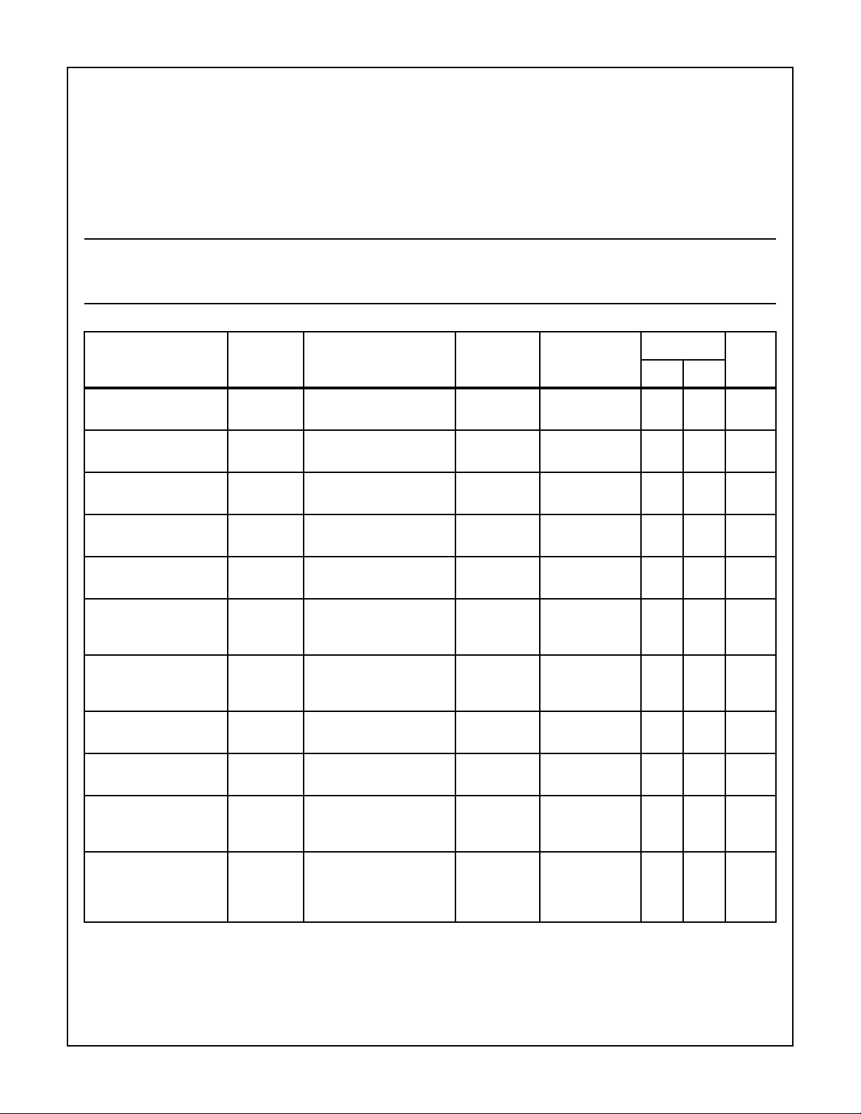
TABLE 1. DC ELECTRICAL PERFORMANCE CHARACTERISTICS
PARAMETER SYMBOL CONDITIONS
Thermal Resistance θ
SBDIP Package. . . . . . . . . . . . . . . . . . . . 40oC/W 6oC/W
Maximum Package Power Dissipation at +125oC Ambient
SBDIP Package. . . . . . . . . . . . . . . . . . . . . . . . . . . . . . . . . .1.25W
If device power exceeds package dissipation capability, provide heat
sinking or derate linearly at the following rate:
SBDIP Package. . . . . . . . . . . . . . . . . . . . . . . . . . . . . . .25.0mW/C
Input Low Voltage . . . . . . . . . . . . . . . . . . . . . . . . . . . . . .0V to +0.8V
Input High Voltage. . . . . . . . . . . . . . . . . . . . . . . . VDD -1.5V to VDD
GROUP A
SUBGROUP TEMPERATURE
JA
LIMITS
θ
JC
UNITSMIN MAX
TTL Output High Voltage VOH1 VDD = 4.5V, IO = -2.5mA,
VIN = 0V, 4.5V
CMOS Output High Voltage
Output Low Voltage VOL VDD = 4.5V, IO = 2.5mA,
Input Leakage Current IIL or IIH VDD = 5.5V, VIN = 0V, 5.5V 1, 2, 3 -55oC, +25oC,
Output Leakage Current IOZL or
Input Current Bus Hold
High
Input Current Bus Hold
Low
Standby Power Supply
Current
Darlington Drive Voltage VDAR VDD = 4.5V, IO = -2.0mA,
Functional Tests FT VDD = 4.5V and 5.5V,
VOH2 VDD = 4.5V, IO = -100µA,
VIN = 0V, 4.5V
VIN = 0V, 4.5V
VDD = 5.5V, VIN = 0V, 5.5V 1, 2, 3 -55oC, +25oC,
IOZH
IBHH VDD = 4.5V or 5.5V,
VIN = 3.0V (See Note 1)
Ports A, B, C
IBHL VDD = 4.5V or 5.5V,
VIN = 1.0V (See Note 2)
Port A
IDDSB VDD = 5.5V, IO = 0mA,
VIN =GND or VDD
VIN = GND or VDD
VIN = GND or VDD,
f = 1MHz
1, 2, 3 -55oC, +25oC,
+125oC
1, 2, 3 -55oC, +25oC,
+125oC
1, 2, 3 -55oC, +25oC,
+125oC
+125oC
+125oC
1, 2, 3 -55oC, +25oC,
+125oC
1, 2, 3 -55oC, +25oC,
+125oC
1, 2, 3 -55oC, +25oC,
+125oC
1, 2, 3 -55oC, +25oC,
+125oC
7, 8A, 8B -55oC, +25oC,
+125oC
3.0 - V
VDD-
0.4
- 0.4 V
-1.0 1.0 µA
-10 10 µA
-800 -60 µA
60 800 µA
-20µA
3.9 - V
-- -
-V
Noise Immunity Functional
Test (Note 4)
NOTES:
1. IBHH should be measured after raising VIN and then lowering to 3.0V.
2. IBHL should be measured after lowering VIN to VSS and then raising to 0.8V.
3. No internal current limiting exists on the Port Outputs. A resistor must be added externally to limit the current.
4. For VIH (VDD = 5.5V) and VIL (VDD = 4.5V) each of the following groups is tested separately with all other inputs using VIH = 2.6V,
VIL = 0.4V: PA, PB, PC, Control Pins (Pins 5, 6, 8, 9, 35, 36).
FN VDD = 5.5V, VIN = GND or
VDD - 1.5V and
VDD = 4.5V, VIN = 0.8V or
VDD
7, 8A, 8B -55oC, +25oC,
+125oC
-- -
Spec Number 518060
972
Specifications HS-82C55ARH
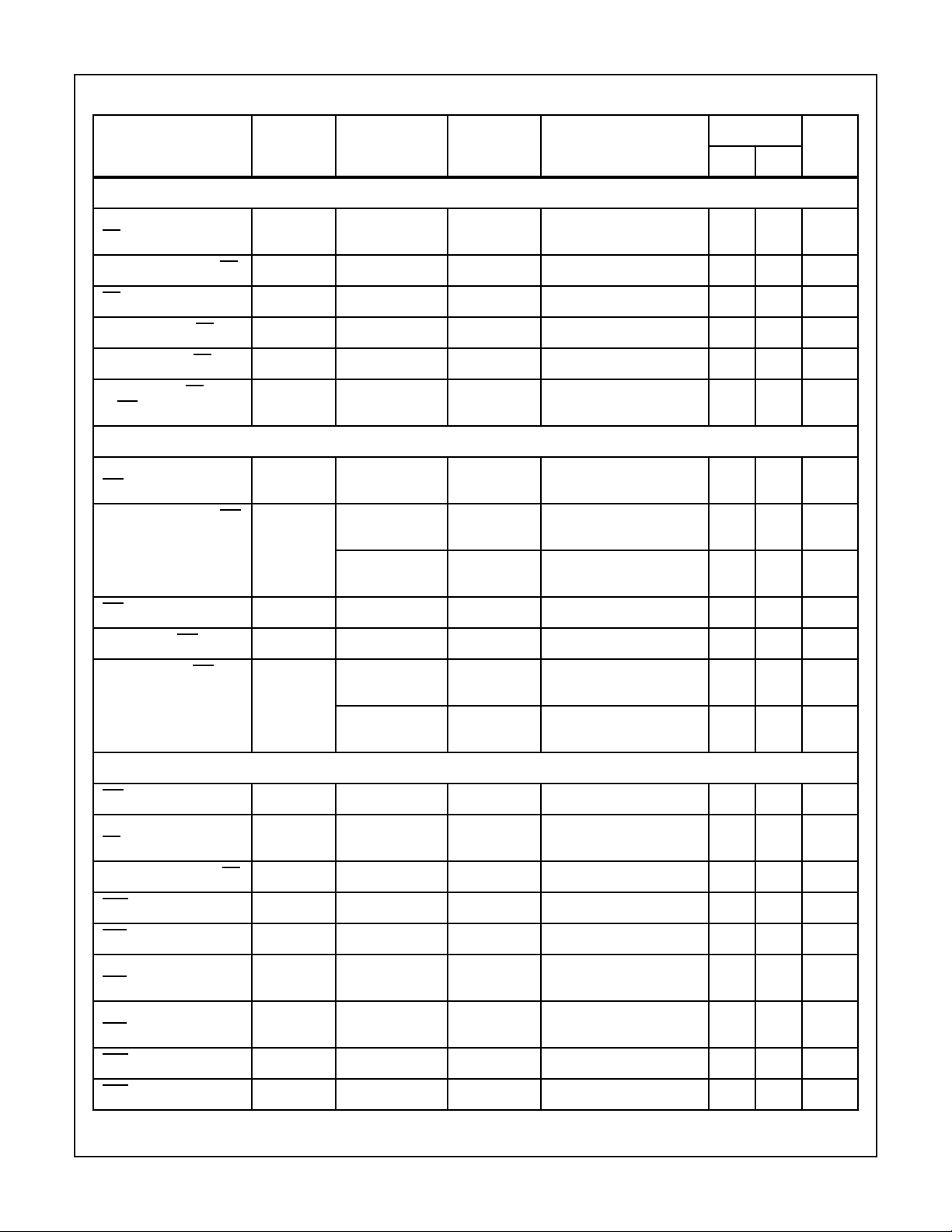
TABLE 2. AC ELECTRICAL PERFORMANCE CHARACTERISTICS TA = -55oC to +125oC
PARAMETER SYMBOL CONDITIONS
READ
SUB-
GROUPS TEMPERATURE
LIMITS
UNITSMIN MAX
Address Stable Before
RD
Address Stable After RD TRHAX VDD = 4.5, 5.5V 9, 10, 11 -55oC, +25oC, +125oC0-ns
RD Pulse Width TRLRH VDD = 4.5, 5.5V 9, 10, 11 -55oC, +25oC, +125oC 250 - ns
Data Valid From RD TRLDV VDD = 4.5, 5.5V 9, 10, 11 -55oC, +25oC, +125oC - 200 ns
Data Float After RD TRHDX VDD = 4.5, 5.5V 9, 10, 11 -55oC, +25oC, +125oC10- ns
Time Between RDs and/
or WRs
WRITE
Address Stable Before
WR
Address Stable After WR TWHAX VDD = 4.5, 5.5V,
WR Pulse Width TWLWH VDD = 4.5, 5.5V 9, 10, 11 -55oC, +25oC, +125oC 100 - ns
Data Valid to WR High TDVWH VDD = 4.5, 5.5V 9, 10, 11 -55oC, +25oC, +125oC 100 - ns
Data Valid After WR High TWHDX VDD = 4.5, 5.5V,
TAVRL VDD = 4.5, 5.5V 9, 10, 11 -55oC, +25oC, +125oC0-ns
TRWHRWL VDD = 4.5, 5.5V 9, 10, 11 -55oC, +25oC, +125oC 300 - ns
TAVWL VDD = 4.5, 5.5V 9, 10, 11 -55oC, +25oC, +125oC0-ns
9, 10, 11 -55oC, +25oC, +125oC20- ns
Ports A and B
VDD = 4.5, 5.5V,
Port C
Ports A and B
9, 10, 11 -55oC, +25oC, +125oC 100 - ns
9, 10, 11 -55oC, +25oC, +125oC30- ns
VDD = 4.5, 5.5V,
Port C
OTHER TIMINGS
WR = 1 to Output TWHPV VDD = 4.5, 5.5V 9, 10, 11 -55oC, +25oC, +125oC - 350 ns
Peripheral Data Before
RD
Peripheral Data After RD TRHPX VDD = 4.5, 5.5V 9, 10, 11 -55oC, +25oC, +125oC0-ns
ACK Pulse Width TKLKH VDD = 4.5, 5.5V 9, 10, 11 -55oC, +25oC, +125oC 200 - ns
STB Pulse Width TSLSH VDD = 4.5, 5.5V 9, 10, 11 -55oC, +25oC, +125oC 100 - ns
Peripheral Data Before
STB High
Peripheral Data After
STB High
ACK = 0 to Output TKLPV VDD = 4.5, 5.5V 9, 10, 11 -55oC, +25oC, +125oC - 175 ns
ACK = 1 to output Float TKHPZ VDD = 4.5, 5.5V 9, 10, 11 -55oC, +25oC, +125oC10- ns
TPVRL VDD = 4.5, 5.5V 9, 10, 11 -55oC, +25oC, +125oC0-ns
TPVSH VDD = 4.5, 5.5V 9, 10, 11 -55oC, +25oC, +125oC20- ns
TSHPX VDD = 4.5, 5.5V 9, 10, 11 -55oC, +25oC, +125oC50- ns
9, 10, 11 -55oC, +25oC, +125oC 100 -
973
Spec Number 518060

Specifications HS-82C55ARH
TABLE 2. AC ELECTRICAL PERFORMANCE CHARACTERISTICS TA = -55oC to +125oC (Continued)
LIMITS
SUB-
PARAMETER SYMBOL CONDITIONS
WR = 1 to OBF = 0 TWHOL VDD = 4.5, 5.5V 9, 10, 11 -55oC, +25oC, +125oC - 150 ns
ACK = 0 to OBF = 1 TKLOH VDD = 4.5, 5.5V 9, 10, 11 -55oC, +25oC, +125oC - 150 ns
STB = 0 to IBF = 1 TSLIH VDD = 4.5, 5.5V 9, 10, 11 -55oC, +25oC, +125oC - 150 ns
RD = 1 to IBF = 0 TRHIL VDD = 4.5, 5.5V 9, 10, 11 -55oC, +25oC, +125oC - 150 ns
RD = 0 to INTR = 1 TRLNL VDD = 4.5, 5.5V 9, 10, 11 -55oC, +25oC, +125oC - 200 ns
STB = 1 t INTR = 1 TSHNH VDD = 4.5, 5.5V 9, 10, 11 -55oC, +25oC, +125oC - 150 ns
ACK = 1 to INTR = 1 TKHNH VDD = 4.5, 5.5V 9, 10, 11 -55oC, +25oC, +125oC - 150 ns
WR = 0 to INTR = 0 TWLNL VDD = 4.5, 5.5V 9, 10, 11 -55oC, +25oC, +125oC - 200 ns
GROUPS TEMPERATURE
UNITSMIN MAX
RESET Pulse Width TRSHRSL VDD = 4.5, 5.5V
(Note 2)
NOTES:
1. AC’s tested at worst case VDD, guaranteed over full operating range.
2. Period of initial RESET pulse after power-on must be at least 50µs. Subsequenct RESET pulses may be 500ns minimum.
TABLE 3. ELECTRICAL PERFORMANCE CHARACTERISTICS
PARAMETER SYMBOL CONDITIONS TEMPERATURE
Input Capacitance CIN VDD = Open, f = 1MHz, All
measurements referenced to
device ground
I/O Capacitance CI/O VDD = Open, f = 1MHz, All
measurements referenced to
device ground
Data Float After RD TRHDX VDD = 4.5V and 5.5V -55oC < TA < +125oC - 75 ns
ACK = 1 to Output Float TKHPZ VDD = 4.5V and 5.5V -55oC < TA < +125oC - 250 ns
NOTE: The parameters listed in Table 3 are controlled via design or process parameters and are not directly tested. These parameters are
characterized upon initial design release and upon design changes which would affect these characteristics
9, 10, 11 -55oC, +25oC, +125oC 500 - ns
LIMITS
UNITSMIN MAX
TA = +25oC - 10 pF
TA = +25oC - 20 pF
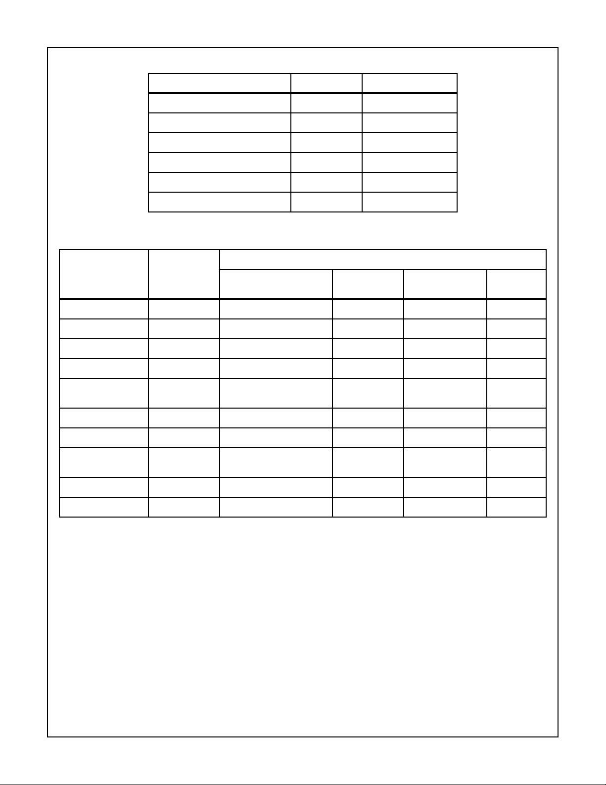
TALBE 4. POST 100K RAD ELECTRICAL PERFORMANCE CHARACTERISTICS
See +25oC limits in Table 1 and Table 2 for Post RAD limits (Subgroups 1, 7, 9)
974
Spec Number 518060
Specifications HS-82C55ARH
TABLE 5. BURN-IN DELTA PARAMETERS (+25oC)
PARAMETER SYMBOL DELTA LIMITS
Static Current IDDSB ±10µA
Input Leakage Current IIL, IIH ±200nA
Output Leakage Current IOZL, IOZH ±2µA
Low Level Output Voltage VOL ±80mV
TTL Output High Voltage VOH1 ±600mV
CMOS Output High Voltage VOH2 ±150mV
TABLE 6. APPLICABLE SUBGROUPS
GROUP A SUBGROUPS
CONFORMANCE
GROUP
Initial Test 100% 5004 1, 7, 9 1 (Note 2) 1, 7, 9
Interim Test 100% 5004 1, 7, 9,∆ 1, ∆ (Note 2) 1, 7, 9
PDA 100% 5004 1, 7, ∆ - 1, 7
Final Test 100% 5004 2, 3, 8A, 8B, 10, 11 - 2, 3, 8A, 8B, 10, 11
Group A (Note 1) Sample 5005 1, 2, 3, 7, 8A, 8B, 9, 10, 11 - 1, 2, 3, 7, 8A, 8B, 9,
Subgroup B5 Sample 5005 1, 2, 3, 7, 8A, 8B, 9, 10, 11, ∆ 1, 2, 3, ∆ (Note 2) N/A
Subgroup B6 Sample 5005 1, 7, 9 - N/A
Group C Sample 5005 N/A N/A 1, 2, 3, 7, 8A, 8B, 9,
Group D Sample 5005 1, 7, 9 - 1, 7, 9
Group E, Subgroup 2 Sample 5005 1, 7, 9 - 1, 7, 9
NOTES:
1. Alternate Group A testing in accordance with MIL-STD-883 method 5005 may be exercised.
2. Table 5 parameters only
MIL-STD-883
METHOD
TESTED FOR -Q
RECORDED
FOR -Q TESTED FOR -8
10, 11
10, 11
RECORDED
FOR -8
975
Spec Number 518060

HS-82C55ARH
Intersil Space Level Product Flow -Q
Wafer Lot Acceptance (All Lots) Method 5007
(Includes SEM)
GAMMA Radiation Verification (Each Wafer) Method 1019,
2 Samples/Wafer, 0 Rejects
100% Die Attach
100% Nondestructive Bond Pull, Method 2023
Sample - Wire Bond Pull Monitor, Method 2011
Sample - Die Shear Monitor, Method 2019 or 2027
100% Internal Visual Inspection, Method 2010, Condition A
CSI and/or GSI PreCap (Note 6)
100% Temperature Cycle, Method 1010, Condition C,
10 Cycles
100% Constant Acceleration, Method 2001, Condition per
Method 5004
100% PIND, Method 2020, Condition A
100% External Visual
100% Serialization
100% Initial Electrical Test (T0)
100% Static Burn-In 1, Condition A or B, 72 Hours Min,
NOTES:
1. Failures from subgroup 1, 7 and deltas are used for calculating PDA. The maximum allowable PDA = 5% with no more than 3% of the
2. Radiographic (X-Ray) inspection may be performed at any point after serialization as allowed by Method 5004.
3. Alternate Group A testing may be performed as allowed by MIL-STD-883, Method 5005.
4. Group B and D inspections are optional and will not be performed unless required by the P.O. When required, the P.O. should include
5. Group D Generic Data, as defined by MIL-I-38535, is optional and will not be supplied unless required by the P.O. When required, the
6. CSI and/or GSI inspections are optional and will not be performed unless required by theP.O. When required, the P.O. should include
7. Data Package Contents:
tity).
o
C Min, Method 1015
+125
failures from subgroup 7.
separate line items for Group B Test, Group B Samples, Group D Test and Group D Samples.
P.O. should include a separate line item for Group D Generic Data. Generic data is not guaranteed to be available and is therefore not
available in all cases.
separate line items for CSI PreCap inspection, CSI final inspection, GSI PreCap inspection, and/or GSI final inspection.
• Cover Sheet (Intersil Name and/or Logo, P.O. Number, Customer Part Number, Lot Date Code, Intersil Part Number, Lot Number, Quan-
• Wafer Lot Acceptance Report (Method 5007). Includes reproductions of SEM photos with percent of step coverage.
• GAMMA Radiation Report. Contains Cover page, disposition, Rad Dose, Lot Number, T est Package used, Specification Numbers, Test
equipment, etc. Radiation Read and Record data on file at Intersil.
• X-Ray report and film. Includes penetrometer measurements.
• Screening, Electrical, and Group A attributes (Screening attributes begin after package seal).
• Lot Serial Number Sheet (Good units serial number and lot number).
• Variables Data (All Delta operations). Data is identified by serial number. Data header includes lot number and date of test.
• Group B and D attributes and/or Generic data is included when required by the P.O.
• The Certificate of Conformance is a part of the shipping invoice and is not part of the Data Book. The Certificate of Conformance is signed
by an authorized Quality Representative.
100% Interim Electrical Test 1 (T1)
100% Delta Calculation (T0-T1)
100% PDA 1, Method 5004 (Note 1)
100% Dynamic Burn-In, Condition D, 240 Hours, +125
Equivalent, Method 1015
100% Interim Electrical Test 2(T2)
100% Delta Calculation (T0-T2)
100% PDA 2, Method 5004 (Note 1)
100% Final Electrical Test
100% Fine/Gross Leak, Method 1014
100% Radiographic (X-Ray), Method 2012 (Note 2)
100% External Visual, Method 2009
Sample - Group A, Method 5005 (Note 3)
Sample - Group B, Method 5005 (Note 4)
Sample - Group D, Method 5005 (Notes 4 and 5)
100% Data Package Generation (Note 7)
CSI and/or GSI Final (Note 6)
o
C or
976
Spec Number 518060
 Loading...