

840
CAUTION: These devices are sensitive to electrostatic discharge; follow proper IC Handling Procedures.
http://www.intersil.com or 407-727-9207
| Copyright © Intersil Corporation 1999
HS-6664RH
Radiation Hardened
8K x 8 CMOS PROM
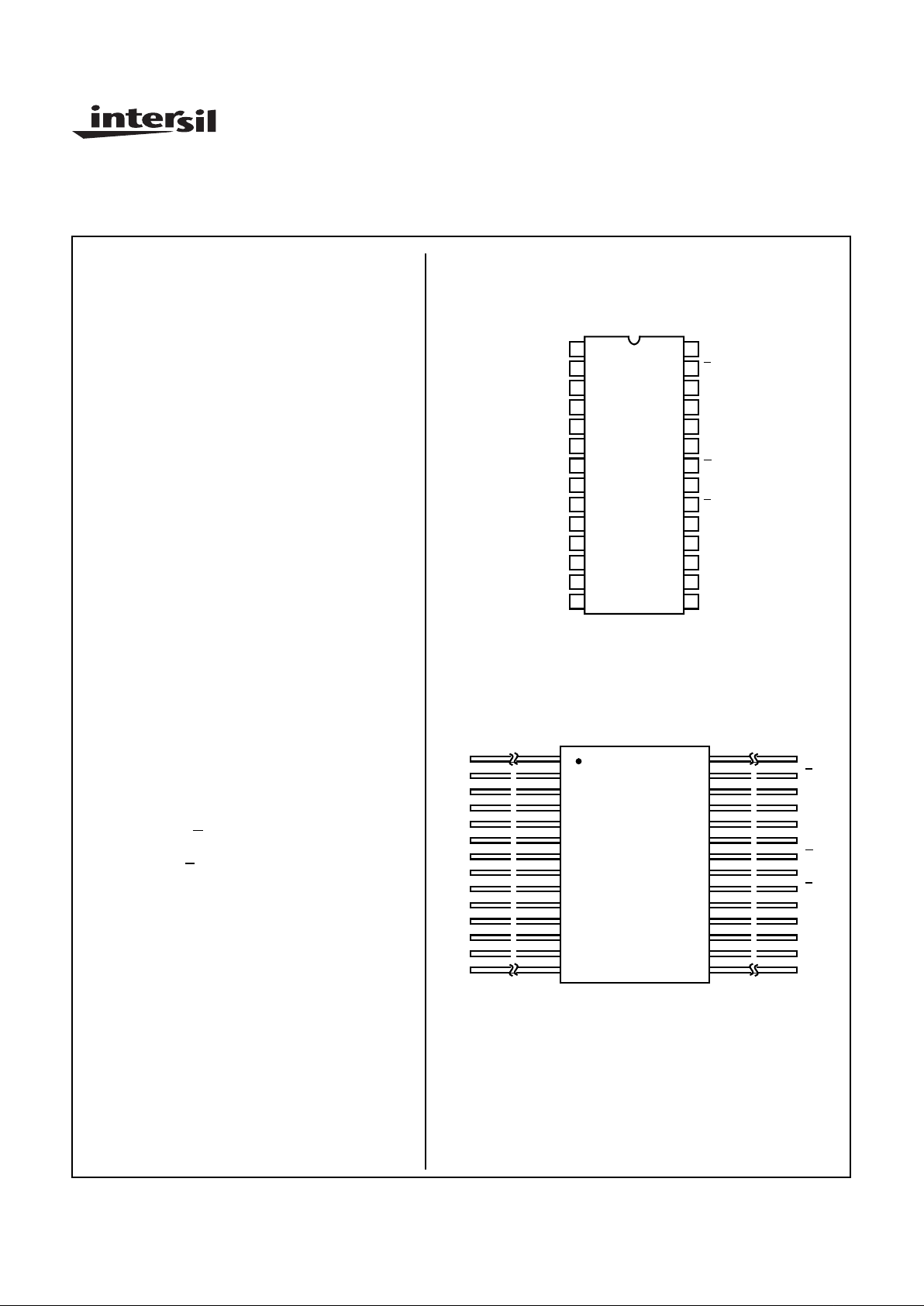
Pinouts
28 LEAD CERAMIC SBDIP
CASE OUTLINE D28.6 MIL-STD-1835, CDIP2-T28
TOP VIEW
28 LEAD FLATPACK
CASE OUTLINE K28.A MIL-STD-1835, CDFP3-F28
TOP VIEW
† P must be hardwired at all times to VDD, except during programming.
NC
A12
A7
A6
A5
A4
A3
A2
A1
A0
DQ0
DQ1
DQ2
GND
VDD
NC
A8
A9
A11
A10
DQ7
DQ6
DQ5
DQ4
DQ3
P †
G
E
28
27
26
25
24
23
22
21
20
19
18
17
16
15
1
2
3
4
5
6
7
8
9
10
11
12
13
14
1
2
3
4
5
6
7
8
9
10
11
12
13
14
28
27
26
25
24
23
22
21
20
19
18
17
16
15
NC
A12
A7
A6
A5
A4
A3
A2
A1
A0
DQ0
DQ1
DQ2
GND
VDD
NC
A8
A9
A11
A10
DQ7
DQ6
DQ5
DQ4
DQ3
P †
G
E
Features
• 1.2 Micron Radiation Hardened Bulk CMOS
• Total Dose 3 x 10
5
RAD (Si)
• Transient Output Upset >5 x 10
8
RAD (Si)/s
• LET >100 MEV-cm
2
/mg
• Fast Access Time - 35ns (Typical)
• Single 5V Power Supply
• Single Pulse 10V Field Programmable
• Synchronous Operation
• On-Chip Address Latches
• Three-State Outputs
• NiCr Fuses
• Low Standby Current <500µA (Pre-Rad)
• Low Operating Current <15mA/MHz
• Military Temperature Range -55
o
C to +125oC
Description
The Intersil HS-6664RH is a radiation hardened 64K
CMOS PROM, organized in an 8K word by 8-bit format. The chip is manufactured using a radiation
hardened CMOS process, and utilizes synchronous
circuit design techniques to achieve high speed
performance with very low power dissipation.
On-chip address latches are provided, allowing easy
interfacing with microprocessors that use a
multiplexed address/data bus structure. The output
enable control (
G) simplifies system interfacing by
allowing output data bus control in addition to the chip
enable control (
E). All bits are manufactured storing a
logical “0” and can be selectively programmed for a
logical “1” at any bit location.
Applications for the HS-6664RH CMOS PROM
include low power microprocessor based instrumentation and communications systems, remote data acquisition and processing systems, and processor control
storage.
September 1995
Spec Number
518741
File Number 3197.3

841
HS-6664RH
Functional Diagram
† P must be hardwired at all times to VDD, except during programming.
TRUTH TABLE
E G MODE
0 0 Enabled
0 1 Output Disabled
1 X Disabled
256 X 256
MATRIX
32 32 32 32 32 32 32 32
256
GATED ROW
DECODER
LATCHED
ADDRESS
REGISTER
8
MSB
A2
A3
A4
A5
A6
A7
A8
LSB
GATED COLUMN DECODER
PROGRAMMING, AND DATA
OUTPUT CONTROL
A
A
8
EE
8
LATCHED ADDRESS
REGISTER
E
E
A
5
A
5
8
1 OF 8
A0 A10 A9 A11 A12
MSB LSB
† P
E
G
Q0 - Q7
A1
Spec Number 518741

842
Specifications HS-6664RH
Absolute Maximum Ratings Reliability Information
Supply Voltage (All Voltages Reference to Device GND). . . . .+7.0V
Input or Output Voltage
Applied for All Grades. . . . . . . . . . . . . . . . . GND-0.3V to VDD+0.3V
Storage Temperature Range . . . . . . . . . . . . . . . . . -65oC to +150oC
Junction Temperature. . . . . . . . . . . . . . . . . . . . . . . . . . . . . . +175oC
Lead Temperature (Soldering 10s). . . . . . . . . . . . . . . . . . . . +300oC
ESD Classification . . . . . . . . . . . . . . . . . . . . . . . . . . . . . . . . Class 1
Thermal Resistance θ
JA
θ
JC
Braze Seal DIP Package. . . . . . . . . . . . . 40.0oC/W 4.0oC/W
Braze Seal Flatpack Package . . . . . . . . . 53.4oC/W 6.0oC/W
Maximum Package Power Dissipation at +125oC
Braze Seal DIP Package. . . . . . . . . . . . . . . . . . . . . . . . . . . 1.75W
Braze Seal Flatpack Package . . . . . . . . . . . . . . . . . . . . . .936mW
Gate Count . . . . . . . . . . . . . . . . . . . . . . . . . . . . . . . . . 26,817 Gates
CAUTION: Stresses above those listed in “Absolute Maximum Ratings” may cause permanent damage to the device. This is a stress only rating and operation
of the device at these or any other conditions above those indicated in the operational sections of this specification is not implied.
Operating Conditions
Operating Supply Voltage Range (VDD) . . . . . . . . . +4.5V to +5.5V
Operating Temperature Range (TA) . . . . . . . . . . . . -55oC to +125oC
Input Low Voltage (VIL). . . . . . . . . . . . . . . . . . . . . . . . . .0V to +0.8V
Input High Voltage (VIH). . . . . . . . . . . . . . . . . . . . . . . +2.4V to VDD
TABLE 1. DC ELECTRICAL PERFORMANCE CHARACTERISTICS
Device Guaranteed and 100% Tested.
PARAMETER SYMBOL
(NOTES 1, 2)
CONDITIONS
GROUP A
SUBGROUPS TEMPERATURE
LIMITS
UNITSMIN MAX
High Level Output
Voltage
VOH1 VDD = 4.5V, IO = -2.0mA 1, 2, 3 -55oC ≤ TA≤ +125oC 3.5 - V
Output High Voltage VOH2 VDD = 4.5V, IO = 100µA 3 -55oC ≤ TA≤ +125oC VDD
-0.3V
-V
Low Level Output
Voltage
VOL VDD = 4.5V, IO = 4.8mA 1, 2, 3 -55oC ≤ TA≤ +125oC - 0.4 V
High Impedance Output
Leakage Current
IOZ VDD = 5.5V, G = 5.5V,
VI/O = GND or VDD
1, 2, 3 -55oC ≤ TA≤ +125oC -10.0 10.0 µA
Input Leakage Current II VDD = 5.5V, VI = GND or
VDD, P Not Tested
1, 2, 3 -55oC ≤ TA≤ +125oC -1.0 1.0 µA
Standby Supply Current IDDSB VDD = 5.5V, IO = 0mA,
VI = VDD or GND
1, 2, 3 -55oC ≤ TA≤ +125oC - 500 µA
Operating Supply
Current
IDDOP VDD = 5.5V, G = VDD,
(Note 3), f = 1MHz,
IO = 0mA, VI = VDD or GND
1, 2, 3 -55oC ≤ TA≤ +125oC - 15 mA
Functional Test FT VDD = 4.5V (Note 4) 7, 8A, 8B -55oC ≤ TA≤ +125oC- - -
NOTES:
1. All voltages referenced to device GND.
2. All tests performed with P hardwired to VDD.
3. Typical derating = 15mA/MHz increase in IDDOP.
4. Tested as follows: f = 1MHz, VIH = 2.4V, VIL = 0.45V, IOH = -1mA, IOL = +1mA, VOH ≥ 1.5V, VOL ≤ 1.5V.
TABLE 2. AC ELECTRICAL PERFORMANCE CHARACTERISTICS
Device Guaranteed and 100% Tested.
PARAMETER SYMBOL
(NOTES 1, 2, 3)
CONDITIONS
GROUP A
SUBGROUPS TEMPERATURE
LIMITS
UNITSMIN MAX
Output Enable Access Time TGLQV VDD = 4.5V and 5.5V 9, 10, 11 -55oC ≤ TA≤ +125oC - 20 ns
Chip Enable Access Time TELQV VDD = 4.5V and 5.5V 9, 10, 11 -55oC ≤ TA≤ +125oC - 60 ns
Address Setup Time TAVEL VDD = 4.5V and 5.5V 9, 10, 11 -55oC ≤ TA≤ +125oC5 - ns
Address Hold Time TELAX VDD = 4.5V and 5.5V 9, 10, 11 -55oC ≤ TA≤ +125oC12 - ns
Spec Number 518741

843
Specifications HS-6664RH
Chip Enable Low Width TELEH VDD = 4.5V and 5.5V 9, 10, 11 -55oC ≤ TA≤ +125oC60 - ns
Chip Enable High Width TEHEL VDD = 4.5V and 5.5V 9, 10, 11 -55oC ≤ TA≤ +125oC20 - ns
Read Cycle Time TELEL VDD = 4.5V and 5.5V 9, 10, 11 -55oC ≤ TA≤ +125oC80 - ns
NOTES:
1. All voltages referenced to device GND.
2. AC measurements assume transition time ≤ 5ns; input levels = 0.0V to 3.0V; timing reference levels = 1.5V; output load = 1 TTLequivalent
load and CL ≥ 50pF.
3. All tests performed with P hardwired to VDD.
4. Address Access Time (TAVQV) = TELQV + TAVEL = 65ns (maximum).
TABLE 3. ELECTRICAL PERFORMANCE CHARACTERISTICS, AC AND DC
PARAMETER SYMBOL
(NOTE 2)
CONDITIONS NOTES TEMPERATURE
LIMITS
UNITSMIN MAX
Input Capacitance CIN VDD = Open, f = 1MHz 1, 3 TA = +25oC - 15 pF
I/O Capacitance CI/O VDD = Open, f = 1MHz 1, 3 TA = +25oC - 12 pF
Chip Enable Time TELQX VDD = 4.5V and 5.5V 3 -55oC ≤ TA≤ +125oC5 - ns
Output Enable Time TGLQX VDD = 4.5V and 5.5V 3 -55oC ≤ TA≤ +125oC5 - ns
Chip Disable Time TEHQZ VDD = 4.5V and 5.5V 3 -55oC ≤ TA≤ +125oC - 15 ns
Output Disable Time TGHQZ VDD = 4.5V and 5.5V 3 -55oC ≤ TA≤ +125oC - 15 ns
NOTES:
1. All measurements referenced to device GND.
2. All tests performed with P hardwired to VDD.
3. The parameters listed are controlled via design or process parameters and are not directly tested. These parameters are characterized
upon initial design and after design or process changes which would affect these characteristics.
TABLE 4. POST 100K RAD AC AND DC ELECTRICAL PERFORMANCE CHARACTERISTICS
NOTE: All AC and DC parameters are tested at the +25oC pre-irradiation limits.
TABLE 5. BURN-IN DELTA PARAMETERS (+25oC)
PARAMETER SYMBOL DELTA LIMITS
Standby Supply Current IDDSB ±50µA
Input Leakage Current IOZ ±1µA
II ±100nA
Output Low Voltage VOL ±60mV
Output High Voltage VOH ±400mV
TABLE 2. AC ELECTRICAL PERFORMANCE CHARACTERISTICS (Continued)
Device Guaranteed and 100% Tested.
PARAMETER SYMBOL
(NOTES 1, 2, 3)
CONDITIONS
GROUP A
SUBGROUPS TEMPERATURE
LIMITS
UNITSMIN MAX
Spec Number 518741

844
Specifications HS-6664RH
Timing Waveform
READ CYCLE
TABLE 6. APPLICABLE SUBGROUPS
CONFORMANCE GROUPS METHOD -Q SUBGROUPS -8 SUBGROUPS
Initial Test 100%/5004 1, 7, 9 1, 7, 9
Interim Test 100%/5004 1, 7, 9 1, 7, 9
PDA 1 and 2 100%/5004 1, 7, ∆ 1, 7
Final Test 100%/5004 2, 3, 8A, 8B, 10, 11 2, 3, 8A, 8B, 10, 11
Group A Samples/5005 1, 2, 3, 7, 8A, 8B, 9, 10, 11 1, 2, 3, 7, 8A, 8B, 9, 10, 11
Group B
(*Optional)
B5 Samples/5005 1, 2, 3, 7, 8A, 8B N/A
Others Samples/5005 1, 7,9 N/A
Group C (Optional) Samples/5005 N/A 1, 7, 9
Group D (Optional) Samples/5005 1, 7, 9 1, 7, 9
Group E, Subgroup 2 (Note 1) Samples/5005 1, 7, 9 1, 7, 9
NOTE:
1. Intersil may exercise its option to perform to a small lot sampling plan of 5 units per lot.
VALID
DATA
TELQX
TGLQX
1.5V 1.5V
TGHQZ
TGLQV
1.5V1.5V
TEHQZ
1.5V
1.5V
TELEH
TEHEL
TELQV
TELAX
TAVEL
TELEL
VALID
ADDRESS
1.5V 1.5V
TAVQV
VALID
ADDRESSES
TS
3.0V
0V
0V
3.0V
0V
3.0V
ADDRESSES
DATA
OUTPUT
G
E
Q0 - Q7
Spec Number 518741
 Loading...