

Intersil Corporation HS-6617RH Datasheet

August 1995
HS-6617RH
Radiation Hardened
2K x 8 CMOS PROM
Features
• Total Dose 1 x 10⁵ RAD (Si)
• Latch-Up Free >1 x 10
• Field Programmable
• Functionally Equivalent to HM-6617
• Pin Compatible with Intel 2716
• Low Standby Power 1.1mW Max
• Low Operating Power 137.5mW/MHz Max
• Fast Access Time 100ns Max
• TTL Compatible Inputs/Outputs
• Synchronous Operation
• On Chip Address Latches
• Three-State Outputs
• Nicrome Fuse Links
• Easy Microprocessor Interfacing
• Military Temperature Range -55
12
RAD (Si)/s
o
C to +125oC
Description
The Intersil HS-6617RH is a radiation hardened 16K CMOS PROM,
organized in a 2K word by 8-bit format. The chip is manufactured
using a radiation hardened CMOS process, and is designed to be
functionally equivalent to the HM-6617. Synchronous circuit design
techniques combine with CMOS processing to give this device high
speed performance with very low power dissipation.
On chip address latches are provided, allowing easy interfacing with
recent generation microprocessors that use multiplexed address/data
bus structure, such as the HS-80C85RH or HS-80C86RH. The output
enable control (
allowing output data bus control, in addition to, the chip enable
control. Synchronous operation of the HS-6617RH is ideal for high
speed pipe-lined architecture systems and also in synchronous logic
replacement functions.
Applications for the HS-6617RH CMOS PROM include low power
microprocessor based instrumentation and communications systems,
remote data acquisition and processing systems, processor control
store, and synchronous logic replacement.
G) simplifies microprocessor system interfacing by
Pinouts
24 LEAD CERAMIC DUAL-IN-LINE
METAL SEAL PACKAGE (SBDIP)
MIL-STD-1835 CDIP2-T24
TOP VIEW
A7
1
2
A6
3
A5
4
A4
5
A3
6
A2
7
A1
8
A0
9
Q0
10
Q1
11
Q2
12
GND
24 LEAD CERAMIC METAL SEAL FLATPACK
PACKAGE (FLATPACK)
MIL-STD-1835 CDFP4-F24
TOP VIEW
A7
A6
A5
A4
A3
A2
A1
A0
Q0
Q1
Q2
GND
1
2
3
4
5
6
7
8
9
10
11
12
24
23
22
21
20
19
18
17
16
15
14
13
24
23
22
21
20
19
18
17
16
15
14
13
VDD
A8
A9
P
G
A10
E
Q7
Q6
Q5
Q4
Q3
VDD
A8
A9
P
G
A10
E
Q7
Q6
Q5
Q4
Q3
Ordering Information
PART NUMBER TEMPERATURE RANGE PACKAGE
HS1-6617RH-Q -55oC to +125oC 24 Lead SBDIP
HS1-6617RH-8 -55oC to +125oC 24 Lead SBDIP
HS1-6617RH/SAMPLE 25oC 24 Lead SBDIP
HS1-6617RH/PROTO -55oC to +125oC 24 Lead SBDIP
HS9-6617RH-Q -55oC to +125oC 24 Lead Flatpack
HS9-6617RH-8 -55oC to +125oC 24 Lead Flatpack
HS9-6617RH/Sample 25oC 24 Lead Flatpack
HS9-6617RH/PROTO -55oC to +125oC 24 Lead Flatpack
CAUTION: These devices are sensitive to electrostatic discharge; follow proper IC Handling Procedures.
http://www.intersil.com or 407-727-9207
| Copyright © Intersil Corporation 1999
1
PIN DESCRIPTION
A Address Input
Q Data Output
E Chip Enable
G Output Enable
P Program Enable (P Hardwired to
VDD, except during programming)
Spec Number
File Number 3033.3
DB NA
518742
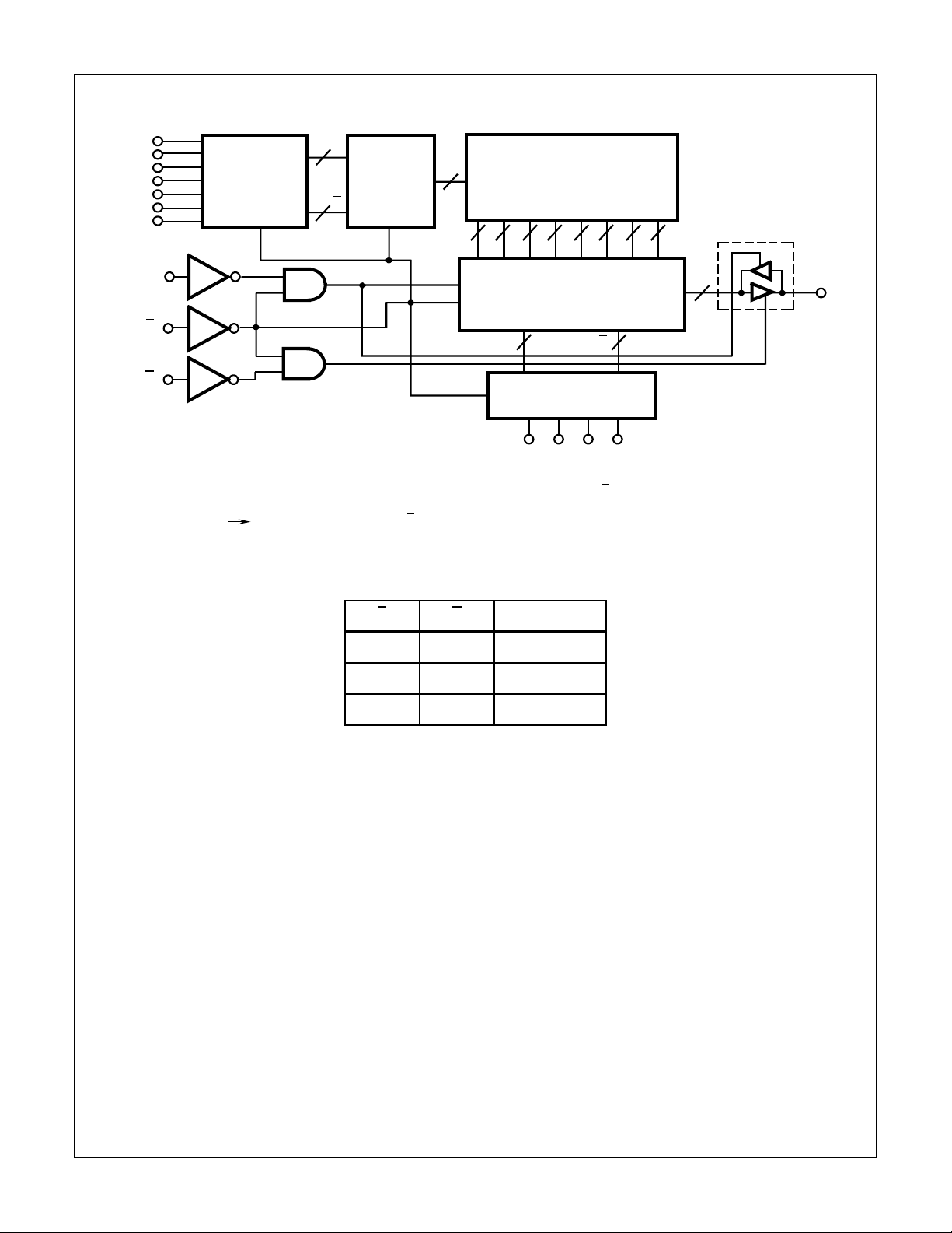
Functional Diagram
MSB
A10
A9
A8
A7
A6
A5
A4
LSB
P
E
LATCHED
ADDRESS
REGISTER
HS-6617RH
7A
7
E
A
GATED
ROW
DECODER
E
128 x 128
MATRIX
128
1 OF 8
16
8
E
GATE COLUMN
DECODER
PROGRAMMING, & DATA
OUTPUT CONTROL
A
4
16 16 161616 16 16
8
A
4
Q0 - Q7
G
ALL LINES POSITIVE LOGIC:
ACTIVE HIGH
THREE STATE BUFFERS:
A HIGH
OUTPUT ACTIVE
E
ADDRESS LATCHES & GATED DECODERS:
LATCH ON FALLING EDGE OF
GATE ON FALLING EDGE OF
P = HARDWIRED TO VDD EXCEPT DURING PROGRAMMING
LATCHED ADDRESS
REGISTER
MSB
A3 A2 A1 A0
LSB
E
G
TRUTH TABLE
E G MODE
0 0 Enabled
0 1 Output Disabled
1 X Disabled
Spec Number 518742
2

Specifications HS-6617RH
Absolute Maximum Ratings Reliability Information
Supply Voltage ( All Voltages Reference to Device GND) . . . .+7.0V
Input or Output Voltage
Applied for All Grades. . . . . . . . . . . . . . . . . GND-0.3V to VDD+0.3V
Storage Temperature Range . . . . . . . . . . . . . . . . . -65oC to +150oC
Junction Temperature. . . . . . . . . . . . . . . . . . . . . . . . . . . . . . +175oC
Lead Temperature (Soldering 10s). . . . . . . . . . . . . . . . . . . . +300oC
ESD Classification . . . . . . . . . . . . . . . . . . . . . . . . . . . . . . . . Class 1
CAUTION: Stresses above those listed in “Absolute Maximum Ratings” may cause permanent damage to the device. This is a stress only rating and operation
of the device at these or any other conditions above those indicated in the operational sections of this specification is not implied.
Operating Conditions
Operating Supply Voltage Range (VDD) . . . . . . . . . +4.5V to +5.5V
Operating Temperature Range (TA) . . . . . . . . . . . . -55oC to +125oC
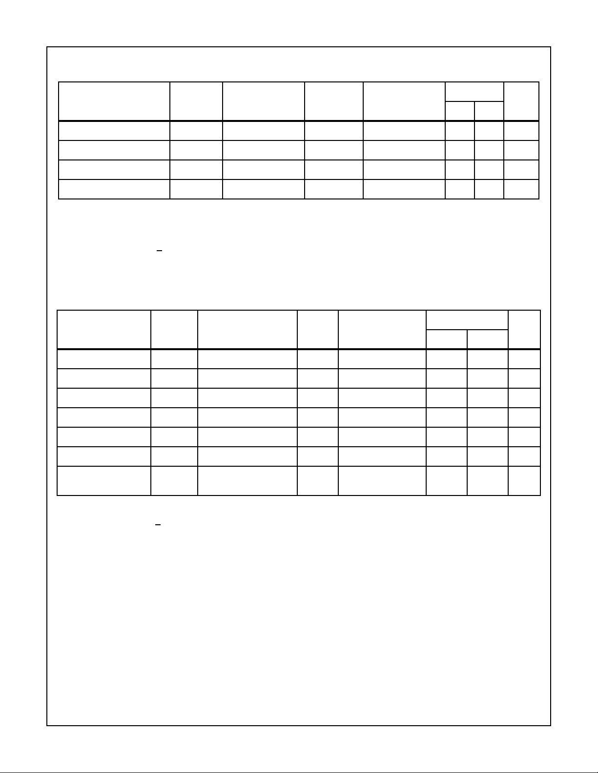
TABLE 1. DC ELECTRICAL PERFORMANCE CHARACTERISTICS
Device Guaranteed and 100% Tested.
Thermal Resistance θ
Sidebraze DIP Package . . . . . . . . . . . . . 40oC/W 6oC/W
Ceramic Flatpack Package . . . . . . . . . . . 60oC/W 4oC/W
Maximum Package Power Dissipation at +125oC
Sidebraze DIP Package . . . . . . . . . . . . . . . . . . . . . . . . . . 1.251W
Ceramic Flatpack Package . . . . . . . . . . . . . . . . . . . . . . . . . 0.83W
If device power exceeds package dissipation capability, provide heat
sinking or derate linearly at the following rate:
Sidebraze DIP Package . . . . . . . . . . . . . . . . . . . . . . . .25.0mW/C
Ceramic Flatpack Package . . . . . . . . . . . . . . . . . . . . . .16.7mW/C
Input Low Voltage (VIL). . . . . . . . . . . . . . . . . . . . . . . . . .0V to +0.8V
Input High Voltage (VIH). . . . . . . . . . . . . . . . . . . . . . . +2.4V to VDD
JA
θ
JC
(NOTES 1, 2)
PARAMETER SYMBOL
High Level Output
Voltage
Low Level Output
Voltage
High Impedance Output
Leakage Current
Input Leakage Current II VDD = 5.5V, VI = GND or
Standby Supply Current IDDSB VDD = 5.5V, IO = 0mA,
Operating Supply
Current
Functional Test FT VDD = 4.5V (Note 4) 7, 8A, 8B -55oC ≤ TA≤ +125oC- - -
NOTES:
1. All voltages referenced to device GND.
2. All tests performed with P hardwired to VDD.
3. Typical derating = 20mA/MHz increase in IDDOP.
4. Tested as follows: f = 1MHz, VIH = 2.4V, VIL = 0.8V, IOH = -1mA, IOL = +1mA, VOH ≥ 1.5V, VOL ≤ 1.5V.
VOH1 VDD = 4.5V, IO = -2.0mA 1, 2, 3 -55oC ≤ TA≤ +125oC 2.4 - V
VOL VDD = 4.5V, IO = 4.8mA 1, 2, 3 -55oC ≤ TA≤ +125oC - 0.4 V
IOZ VDD = 5.5V, G = 5.5V,
IDDOP VDD = 5.5V, G = GND,
CONDITIONS
VI/O = GND or VDD
VDD, P Not Tested
VI = VDD or GND
(Note 3), f = 1MHz,
IO = 0mA, VI = VDD or GND
GROUP A
SUBGROUPS TEMPERATURE
1, 2, 3 -55oC ≤ TA≤ +125oC -10.0 10.0 µA
1, 2, 3 -55oC ≤ TA≤ +125oC -1.0 1.0 µA
1, 2, 3 -55oC ≤ TA≤ +125oC - 200 µA
1, 2, 3 -55oC ≤ TA≤ +125oC - 25 mA
LIMITS
UNITSMIN MAX
TABLE 2. AC ELECTRICAL PERFORMANCE CHARACTERISTICS
Device Guaranteed and 100% Tested.
LIMITS
(NOTES 1, 2, 3)
PARAMETERS SYMBOL
Address Access Time TAVQV VDD = 4.5V and 5.5V
Output Enable Access Time TGLQV VDD = 4.5V and 5.5V 9, 10, 11 -55oC ≤ TA≤ +125oC - 50 ns
Chip Enable Access Time TELQV VDD = 4.5V and 5.5V 9, 10, 11 -55oC ≤ TA≤ +125oC - 100 ns
Address Setup Time TAVEL VDD = 4.5V and 5.5V 9, 10, 11 -55oC ≤ TA≤ +125oC20 - ns
CONDITIONS
(Note 4)
GROUP A
SUBGROUPS TEMPERATURE
9, 10, 11 -55oC ≤ TA≤ +125oC - 120 ns
UNITSMIN MAX
Spec Number 518742
3
Specifications HS-6617RH
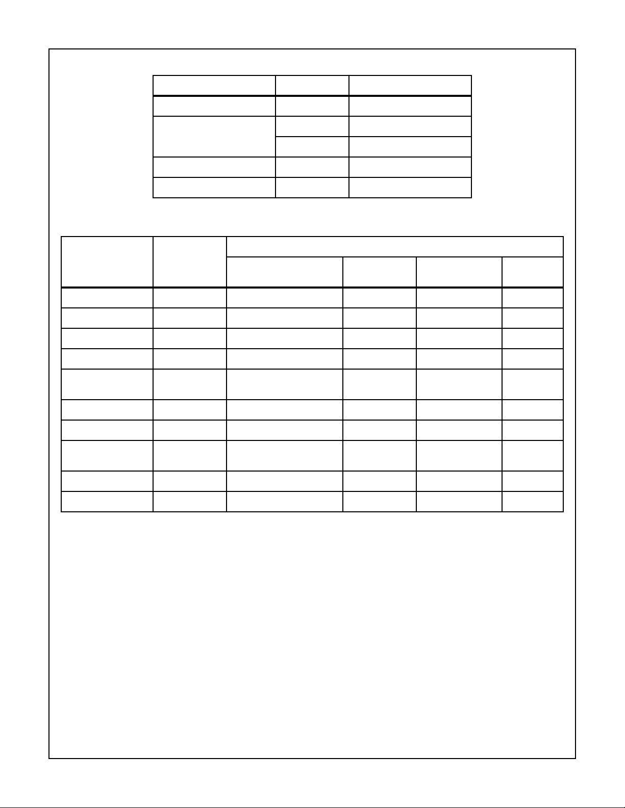
TABLE 2. AC ELECTRICAL PERFORMANCE CHARACTERISTICS (Continued)
Device Guaranteed and 100% Tested.
LIMITS
(NOTES 1, 2, 3)
PARAMETERS SYMBOL
Address Hold Time TELAX VDD = 4.5V and 5.5V 9, 10, 11 -55oC ≤ TA≤ +125oC25 - ns
Chip Enable Low Width TELEH VDD = 4.5V and 5.5V 9, 10, 11 -55oC ≤ TA≤ +125oC 120 - ns
Chip Enable High Width TEHEL VDD = 4.5V and 5.5V 9, 10, 11 -55oC ≤ TA≤ +125oC40 - ns
Read Cycle Time TELEL VDD = 4.5V and 5.5V 9, 10, 11 -55oC ≤ TA≤ +125oC 160 - ns
NOTES:
1. All voltages referenced to device GND.
2. AC measurements assume transition time≤ 5ns; input levels = 0.0V to 3.0V; timing reference levels = 1.5V; output load = 1 TTL equivalent
load and CL ≥ 50pF.
3. All tests performed with P hardwired to VDD.
4. TAVQV = TELQV + TAVEL.
TABLE 3. ELECTRICAL PERFORMANCE CHARACTERISTICS, AC AND DC
CONDITIONS
GROUP A
SUBGROUPS TEMPERATURE
UNITSMIN MAX
LIMITS
(NOTE 2)
PARAMETERS SYMBOL
Input Capacitance CIN VDD = Open, f = 1MHz 1, 3 TA = +25oC - 10 pF
I/O Capacitance CI/O VDD = Open, f = 1MHz 1, 3 TA = +25oC - 12 pF
Chip Enable Time TELQX VDD = 4.5V and 5.5V 3 -55oC ≤ TA≤ +125oC5 - ns
Output Enable Time TGLQX VDD = 4.5V and 5.5V 3 -55oC ≤ TA≤ +125oC5 - ns
Chip Disable Time TEHQZ VDD = 4.5V and 5.5V 3 -55oC ≤ TA≤ +125oC - 50 ns
Output Disable Time TGHQZ VDD = 4.5V and 5.5V 3 -55oC ≤ TA≤ +125oC - 50 ns
Output High Voltage VOH2 VDD = 4.5V, IO = 100µA 3 -55oC ≤ TA≤ +125oC VDD-
NOTES:
1. All measurements referenced to device GND.
2. All tests performed with P hardwired to VDD.
3. The parameters listed are controlled via design or process parameters and are not directly tested. These parameters are characterized
upon initial design and after design or process changes which would affect these characteristics.
TABLE 4. POST 100K RAD AC AND DC ELECTRICAL PERFORMANCE CHARACTERISTICS
CONDITIONS NOTES TEMPERATURE
UNITSMIN MAX
-V
0.5V
NOTE: All AC and DC parameters are tested at the +25oC pre-irradiation limits.
4
Spec Number 518742
HS-6617RH
TABLE 5. BURN-IN DELTA PARAMETERS (+25oC)
PARAMETER SYMBOL DELTA LIMITS
Standby Supply Current IDDSB ±10µA
Input Leakage Current IOZ ± 1µA
II ±100nA
Output Low Voltage VOL ± 60mV
Output High Voltage VOH ± 400mV
TABLE 6. APPLICABLE SUBGROUPS
GROUP A SUBGROUPS
CONFORMANCE
GROUP
Initial Test 100% 5004 1, 7, 9 1 (Note 2) 1, 7, 9
Interim Test 100% 5004 1, 7, 9, ∆ 1, ∆ (Note 2) 1, 7, 9
PDA 100% 5004 1, 7, ∆ - 1, 7
Final Test 100% 5004 2, 3, 8A, 8B, 10, 11 - 2, 3, 8A, 8B, 10, 11
Group A (Note 1) Sample 5005 1, 2, 3, 7, 8A, 8B, 9, 10, 11 - 1, 2, 3, 7, 8A, 8B, 9,
Subgroup B5 Sample 5005 1, 2, 3, 7, 8A, 8B, 9, 10, 11, ∆ 1, 2, 3, ∆ (Note 2) -
Subgroup B6 Sample 5005 1, 7, 9 - -
Group C Sample 5005 - - 1, 2, 3, 7, 8A, 8B, 9,
Group D Sample 5005 1, 7, 9 - 1, 7, 9
Group E, Subgroup 2 Sample 5005 1, 7, 9 - 1, 7, 9
NOTES:
1. Alternate Group A testing in accordance with MIL-STD-883 method 5005 may be exercised.
2. Table 5 parameters only
MIL-STD-883
METHOD
TESTED FOR -Q
RECORDED
FOR -Q TESTED FOR -8
10, 11
10, 11
RECORDED
FOR -8
Spec Number 518742
5
 Loading...