

Intersil Corporation HS-565ARH Datasheet

March 1996
Semiconductor
HS-565ARH
Radiation Hardened High Speed,
Monolithic Digital-to-Analog Converter
Features
• Devices QML Qualified in Accordance with
MIL-PRF-38535
• Detailed Electrical and Screening Requirements
are Contained in SMD# 5962-96755 and Harris’ QM
Plan
• DAC and Reference on a Single Chip
• Pin Compatible with AD-565A and HI-565A
• Very High Speed: Settles to 0.50 LSB in 500ns Max
• Monotonicity Guaranteed Over Temperature
• 0.50 LSB Max Nonlinearity Guaranteed Over
Temperature
• Low Gain Drift (Max., DAC Plus Ref erence) 50ppm/
o
C
• Total Dose Hardness to 100K RAD
• ±0.75 LSB Accuracy Guaranteed Over Temperature
(±0.125 LSB Typical at +25oC)
Applications
• High Speed A/D Converters
• Precision Instrumentation
• Signal Reconstruction
Description
The HS-565ARH is a fast, radiation hardened 12-bit current output, digital-to-analog converter. The monolithic chip includes a
precision voltage reference, thin-film R-2R ladder, reference
control amplifier and twelve high-speed bipolar current
switches.
The Harris Semiconductor Dielectric Isolation process provides
latch-up free operation while minimizing stray capacitance and
leakage currents, to produce an excellent combination of speed
and accuracy. Also, g round currents are minimized to produce a
low and constant current through the ground terminal, which
reduces error due to code-dependent ground currents.
HS-565ARH die are laser trimmed for a maximum integral nonlinearity error of ±0.25 LSB at +25
o
C. In addition, the low noise buried zener reference is trimmed both for absolute v alue and minimum temperature coefficient.
Functional Diagram
9.95K
IO
BIP.
OFF.
8
5K
5K
2.5K
11
10
9
20V
SPAN
10V
SPAN
OUT
REF OUT VCC
6
REF
IN
5
REF
GND
43
+
-
19.95K
10V
3.5K
3K
IREF
0.5mA
+
-
DAC
(4X IREF
X CODE)
712
-VEE PWR
Ordering Information
PART NUMBER TEMPERA TURE RANGE SCREENING LEVEL PACKAGE
5962R9675501VJC
5962R9675501VXC
HS1-565ARH (SAMPLE)
HS9-565ARH (SAMPLE)
CAUTION: These devices are sensitive to electrostatic discharge. Users should follow proper IC Handling Procedures.
Copyright
© Harris Corporation 1996
-55oC to +125oC MIL-PRF-38535 Level V 24 Lead SBDIP
-55oC to +125oC MIL-PRF-38535 Level V 24 Lead Ceramic Flatpack
+25oC Sample 24 Lead SBDIP
+25oC Sample 24 Lead Ceramic Flatpack
1
GND
24 . . . 13
MSB LSB
Spec Number 518795
File Number 3278.2
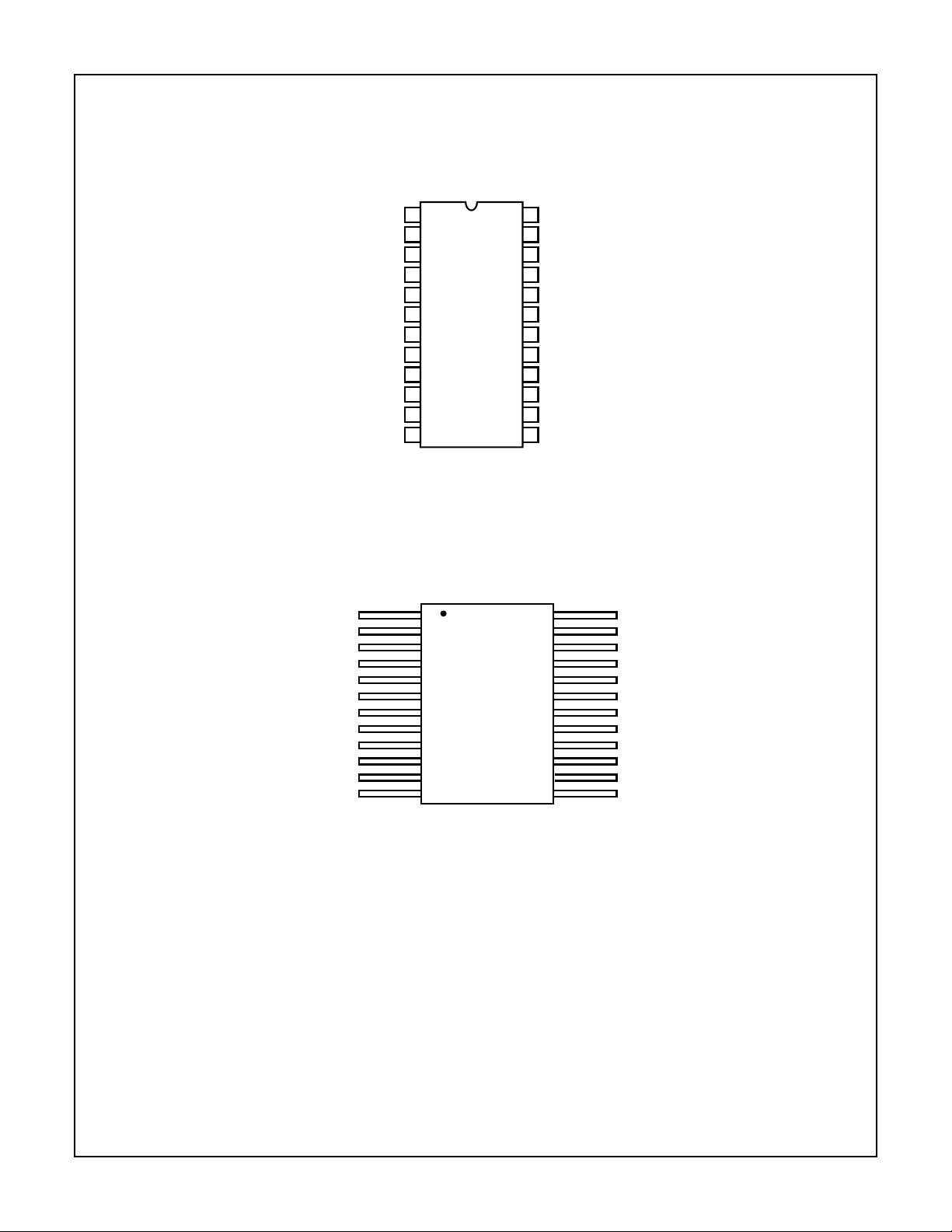
Pinouts
HS-565ARH
HS1-565ARH
MIL-STD-1835 CDIP2-T24
(SBDIP)
TOP VIEW
BIPOLAR RIN
NC
NC
VCC
REF OUT
REF GND
REF IN
-VEE
BIPOLAR RIN
IDAC OUT
10V SPAN
20V SPAN
PWR GND
NC
NC
VCC
REF OUT
REF GND
REF IN
-VEE
IDAC OUT
10V SPAN
20V SPAN
PWR GND
1
2
3
4
5
6
7
8
9
10
11
12
24
23
22
21
20
19
18
17
16
15
14
13
H59-565ARH
MIL-STD-1835 CDFP4-F24
(CERAMIC FLATPACK)
TOP VIEW
1
2
3
4
5
6
7
8
9
10
11
12
24
23
22
21
20
19
18
17
16
15
14
13
BIT 1 IN (MSB)
BIT 2 IN
BIT 3 IN
BIT 4 IN
BIT 5 IN
BIT 6 IN
BIT 7 IN
BIT 8 IN
BIT 9 IN
BIT 10 IN
BIT 11 IN
BIT 12 IN (LSB)
BIT 1 IN
(MSB)
BIT 2 IN
BIT 3 IN
BIT 4 IN
BIT 5 IN
BIT 6 IN
BIT 7 IN
BIT 8 IN
BIT 9 IN
BIT 10 IN
BIT 11 IN
BIT 12 IN
(LSB)
Spec Number 518795
2
Specifications HS-565ARH
Absolute Maximum Ratings Thermal Information
VCC to Power Ground . . . . . . . . . . . . . . . . . . . . . . . . . . 0V to +18V
VEE to Power Ground . . . . . . . . . . . . . . . . . . . . . . . . . . . 0V to -18V
Voltage on DAC Output (Pin 9). . . . . . . . . . . . . . . . . . . . -3V to +12V
Digital Input (Pins 13 - 24) to Power Ground . . . . . . . . . . -1V to +7V
Ref In to Reference Ground . . . . . . . . . . . . . . . . . . . . . . . . . . . . . . ±12V
Bipolar Offset to Reference Ground . . . . . . . . . . . . . . . . . . . . . . . ±12V
10V Span R to Reference Ground. . . . . . . . . . . . . . . . . . . . . . . . . ±12V
20V Span R to Reference Ground. . . . . . . . . . . . . . . . . . . . . . . . . ±24V
Junction Temperature (TJ) (Max) . . . . . . . . . . . . . . . . . . . . . +175oC
Storage Temperature Range . . . . . . . . . . . . . . . . . -65oC to +150oC
Lead Temperature (Soldering 10s). . . . . . . . . . . . . . . . . . . . +300oC
CAUTION: Stresses above those listed in “Absolute Maximum Ratings” may cause permanent damage to the device. This is a stress only rating and operation
of the device at these or any other conditions above those indicated in the operational sections of this specification is not implied.
Operating Conditions
Operating Voltage Range (VCC) . . . . . . . . . . . . . +11.4V to +16.5V
Operating Voltage Range (VEE). . . . . . . . . . . . . . . -11.4V to -16.5V
Operating Temperature Range. . . . . . . . . . . . . . . . -55oC to +125oC
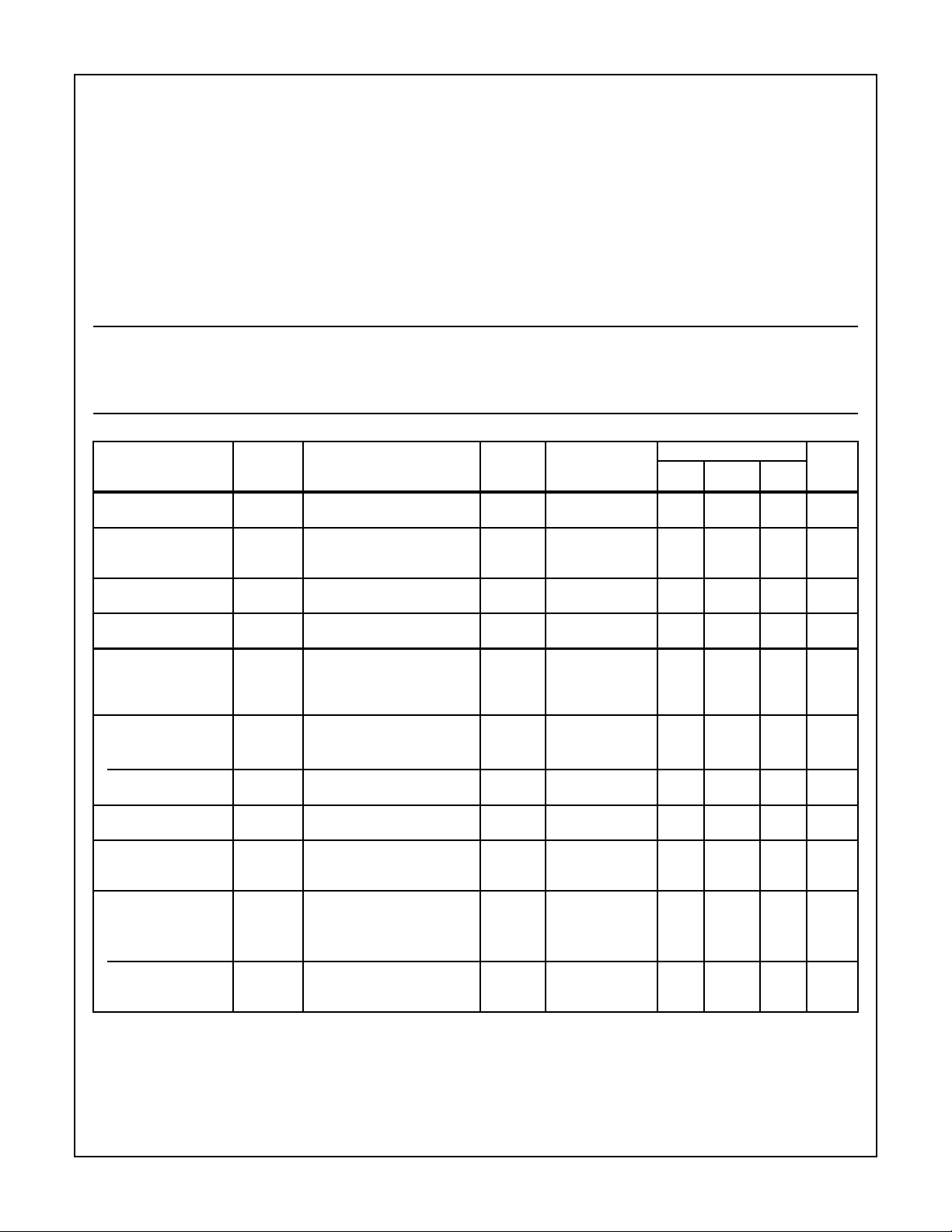
TABLE 1. DC ELECTRICAL PERFORMANCE CHARACTERISTICS
PARAMETERS SYMBOL CONDITIONS
Resolution VSSD = VSSA = 0V,
VCC = +15V, VEE = -15V
Accuracy ILE VSSD = VSSA = 0V,
VCC = +15V, VEE = -15V,
Error Relative to Full Scale
Digital Input High Current IIH VSSD = VSSA = 0V , VIN = 5.5V
VCC = +15V, VEE = -15V
Digital Input Low Current IIL VSSD = VSSA = 0V, V
VCC = +15V, VEE = -15V
Differential Nonlinearity DLE VSSD = VSSA = 0V,
VCC = +15V, VEE = -15V,
o
+25
C (Monotonicity
Guaranteed Over Temp)
Power Supply Currents
VCC ICC VSSD = VSSA = 0V,
VCC = +15V, VEE = -15V
VEE IEE VSSD = VSSA = 0V,
VCC = +15V, VEE = -15V
Reference Output
Voltage
Reference Output
Current
Ref Out VSSD = VSSA = 0V,
VCC = +15V, VEE = -15V
IREF VSSD = VSSA = 0V,
VCC = +15V, VEE = -15V,
Availab le for external loads
Output Current
Unipolar I
OUT1
VSSD = VSSA = 0V,
VCC = +15V, VEE = -15V,
All Bits On
Bipolar I
OUT2
VSSD = VSSA = 0V,
VCC = +15V, VEE = -15V,
All Bits On or Off
IN
= 0V
Thermal Resistance (Typical) θJA(oC/W) θJC(oC/W)
SBDIP Package. . . . . . . . . . . . . . . . . . 60 17
Ceramic Flatpack Package 80 15
Maximum Package Power Dissipation at +125oC
SBDIP Package. . . . . . . . . . . . . . . . . . . . . . . . . . . . . . . . . . 0.83W
Ceramic Flatpack Package . . . . . . . . . . . . . . . . . . . . . . . . . 0.62W
If Device Power Exceeds Package Dissipation Capability, Provide
Heat Sinking or Derate Linearly at the Following Rate:
SBDIP Package 16.67mW/oC
Ceramic Flatpack Package 12.5mW/oC
Digital Input Low Voltage. . . . . . . . . . . . . . . . . . . . . . . . .0V to +0.8V
Digital Input High Voltage . . . . . . . . . . . . . . . . . . . . . +2.2V to +5.5V
GROUP A
LIMITS
SUB-
GROUP TEMPERATURE
1, 2, 3 -55
1, 2, 3 -55
1, 2, 3 -55
o
C to +125oC - - 12 Bits
o
C to +125oC-±0.125 ±0.75 LSB
o
C to +125oC - 0.01 +1.0 µA
UNITSMIN TYP MAX
1, 2, 3 -55oC to +125oC -20 -2.0 - µA
1, 2, 3 -55oC to +125oC- ±0.25 ±0.50 LSB
1, 2, 3 -55
1, 2, 3 -55
1, 2, 3 -55
1, 2, 3 -55
o
C to +125oC - 9.0 11.8 mA
o
C to +125oC -14.5 -9.5 - mA
o
C to +125oC 9.9 10 10.1 V
o
C to +125oC 1.5 2.5 - mA
1, 2, 3 -55oC to +125oC -1.6 -2.0 -2.4 mA
1, 2, 3 -55oC to +125oC ±0.8 ±1.0 ±1.2 mA
Spec Number 518795
3
 Loading...