

February 1996
HS-54C138RH
Radiation Hardened
3-Line to 8-Line Decoder/Demultiplexer
Features
• Devices QML Qualified in Accordance With
MIL-PRF-38535
• Detailed Electrical and Screening Requirements are
Contained in SMD# 5962-95825 and Intersil’ QM Plan
• Radiation Hardened EPI-CMOS
- Total Dose 1 x 10
- Latch-Up Immune > 1 x 10
5
RAD (Si)
12
RAD (Si)/s
• Multiple Input Enable for Easy Expansion
• Single Power Supply +5V
• Outputs Active Low
• Low Standby Power (0.5mW Max at +5V)
• High Noise Immunity
• Equivalent to Sandia SA2995
• Bus Compatible with Intersil Rad-Hard 80C85RH
o
• Full Military Temperature Range -55
C to +125oC
Description
The Intersil HS-54C138RH is a radiation hardened 3- to 8-line
decoder fabricated using a radiation hardened EPI-CMOS process. It features low power consumption, high noise immunity,
and high speed. Also featured are pin and function compatibility
with the 54LS138 industry standard part. The HS-54C138RH is
ideally suited for high speed memory chip select address
decoding. It is intended for use with the Intersil HS-80C85RH
radiation hardened microprocessor, b ut it can also be utilized as
a demultiplexer in an y lo w po wer r ad-hard application.
The HS-54C138RH contains a one of eight binary decoder.
A three bit binary input is used to select and activate each of
the eight outputs, provided the three chip enable inputs are
also present (see truth table).
The HS-54C138RH has an on-chip enable gate. The active
high (G1) and both active low (
together to provide a single enable input to the device. The
use of both active high and active low inputs minimizes the
need for external gates when expanding a system.
G2A, G2B) inputs are Anded
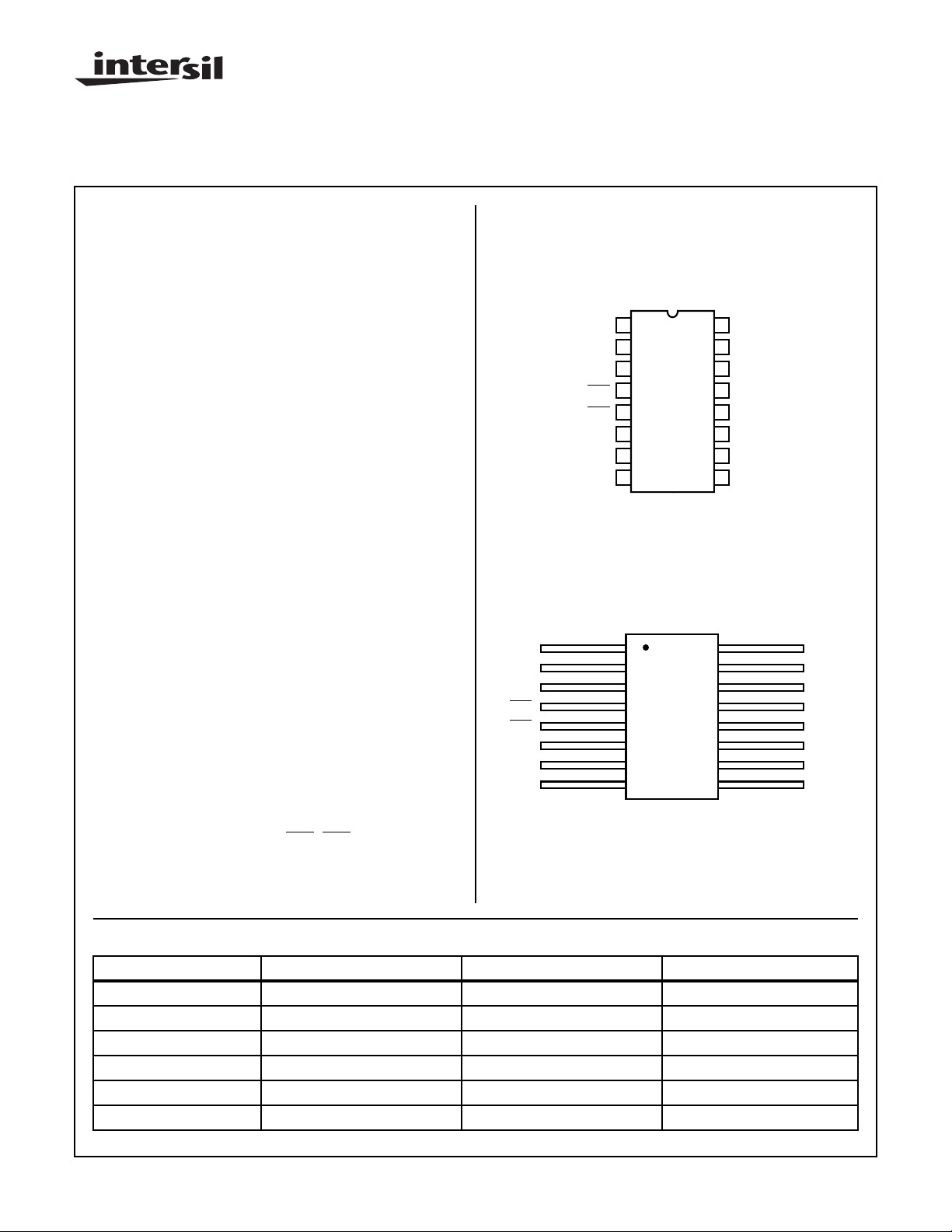
Pinouts
A
B
C
G2A
G2B
G1
Y7
GND
16 LEAD CERAMIC DUAL-IN-LINE
METAL SEAL PACKAGE (SBDIP)
MIL-STD-1835 CDIP2-T16
TOP VIEW
16
1
A
2
B
3
C
4
G2A
5
G2B
6
G1
7
Y7
8
GND
16 LEAD CERAMIC METAL SEAL
FLATPACK PACKAGE (FLATPACK)
MIL-STD-1835 CDFP4-F16
TOP VIEW
116
2
3
4
5
6
7
8
VDD
15
Y0
14
Y1
13
Y2
12
Y3
11
Y4
10
Y5
9
Y6
15
14
13
12
11
10
9
VDD
Y0
Y1
Y2
Y3
Y4
Y5
Y6
Ordering Information
PART NUMBER TEMPERATURE RANGE SCREENING LEVEL PACKAGE
5962R9582501QEC -55oC to +125oC MIL-PRF-38535 Level Q 16 Lead SBDIP
5962R9582501QXC -55oC to +125oC MIL-PRF-38535 Level Q 16 Lead Ceramic Flatpack
5962R9582501VEC -55oC to +125oC MIL-PRF-38535 Level V 16 Lead SBDIP
5962R9582501VXC -55oC to +125oC MIL-PRF-38535 Level V 16 Lead Ceramic Flatpack
HS1-54C138RH/SAMPLE +25oC Sample 16 Lead SBDIP
HS9-54C138RH/SAMPLE +25oC Sample 16 Lead Ceramic Flatpack
CAUTION: These devices are sensitive to electrostatic discharge; follow proper IC Handling Procedures.
http://www.intersil.com or 407-727-9207
| Copyright © Intersil Corporation 1999
1
Spec Number
File Number 3037.2
518053
Specifications HS-54C138RH
Absolute Maximum Ratings Reliability Information
Supply Voltage . . . . . . . . . . . . . . . . . . . . . . . . . . . . . . . . . . . . .+7.0V
I/O Voltage Applied. . . . . . . . . . . . . . . . . . GND -0.3V to VDD +0.3V
Storage Temperature Range . . . . . . . . . . . . . . . . . -65oC to +150oC
Junction Temperature. . . . . . . . . . . . . . . . . . . . . . . . . . . . . . +175oC
Lead Temperature (Soldering 10s). . . . . . . . . . . . . . . . . . . . +300oC
ESD Classification . . . . . . . . . . . . . . . . . . . . . . . . . . . . . . . . Class 1
CAUTION: Stresses above those listed in “Absolute Maximum Ratings” may cause permanent damage to the device. This is a stress only rating and operation
of the device at these or any other conditions above those indicated in the operational sections of this specification is not implied.
Operating Conditions
Operating Voltage Range . . . . . . . . . . . . . . . . . . . +4.75V to +5.25V
Operating Temperature Range. . . . . . . . . . . . . . . . -55oC to +125oC
TABLE 1. DC ELECTRICAL PERFORMANCE CHARACTERISTICS
Thermal Resistance θ
SBDIP Package. . . . . . . . . . . . . . . . . . . . 73oC/W 24oC/W
Ceramic Flatpack Package . . . . . . . . . . . 114oC/W 29oC/W
Maximum Package Power Dissipation at +125oC Ambient
SBDIP Package. . . . . . . . . . . . . . . . . . . . . . . . . . . . . . . . . .0.68W
Ceramic Flatpack Package . . . . . . . . . . . . . . . . . . . . . . . . .0.44W
If device power e xceeds package dissipation capability, provide heat
sinking or derate linearly at the following rate:
SBDIP Package. . . . . . . . . . . . . . . . . . . . . . . . . . . . . .13.7mW/oC
Ceramic Flatpack Package . . . . . . . . . . . . . . . . . . . . . .8.8mW/oC
Input Low Voltage . . . . . . . . . . . . . . . . . . . . . . . . . . . . . . .0V to 1.0V
Input High Voltage. . . . . . . . . . . . . . . . . . . . . . . . .VDD-1.0V to VDD
JA
θ
JC
GROUP A
PARAMETER SYMBOL CONDITIONS
Input Leakage Current
High
Input Leakage Current
Low
High Level Output
Voltage
Low Level Output
Voltage
Static Current SIDD VDD = 5.25V, VIN = GND 1, 2, 3 -55oC, +25oC,
Functional Tests FT VDD = 5.25V and 4.75V,
NOTE: All devices are guaranteed at worst case limits and conditions.
PARAMETER SYMBOL
SELECT TO OUTPUT PROPAGATION DELAY TIME
IIH VDD = 5.25V, VIN = 0V,
Pin Under Test = VDD
IIL VDD = 5.25V, VIN = 5.25V,
Pin Under Test = 0V
VOH VDD = 4.75V, IIN = -2mA 1, 2, 3 -55oC, +25oC,
VOL VDD = 5.25V, IIN = 2mA 1, 2, 3 -55oC, +25oC,
VIH = VDD - 1.0V, VIL = 1.0V
TABLE 2. AC ELECTRICAL PERFORMANCE CHARACTERISTICS
GROUP A SUB-
GROUPS TEMPERATURE
SUBGROUPS TEMPERATURE
1, 2, 3 -55oC, +25oC,
+125oC
1, 2, 3 -55oC, +25oC-1 - µA
+125oC
+125oC
+125oC
7, 8A, 8B -55oC, +25oC,
+125oC
LIMITS
UNITSMIN MAX
-1µA
4.25 - V
0.5 - V
- 100 µA
-- -
LIMITS
UNITSMIN MAX
Low to high level input, High to
low level output
Low to high level input, Low to
high level output
High to low level input, Low to
high level output
High to low level input, high to
low level output
ENABLE TO OUTPUT PROPAGATION DELAY TIME
Low to high level input, Low to
high level output
TPHL11 9, 10, 11 -55oC, +25oC, +125oC - 110 ns
TPLH11 9, 10, 11 -55oC, +25oC, +125oC - 65 ns
TPLH12 9, 10, 11 -55oC, +25oC, +125oC - 75 ns
TPHL12 9, 10, 11 -55oC, +25oC, +125oC - 90 ns
TPLH21 9, 10, 11 -55oC, +25oC, +125oC - 70 ns
Spec Number 518053
2

HS-54C138RH
TABLE 2. AC ELECTRICAL PERFORMANCE CHARACTERISTICS (Continued)
GROUP A SUB-
PARAMETER SYMBOL
Low to high level input, High to
low level output
High to low level input, Low to
high level output
High to low level input, High to
low level output
NOTE: Output timings are measured with a capacitive load, CL = 100pF, VIH = 3.75V, and VIL = 1.0V.
PARAMETER SYMBOL CONDITIONS TEMPERATURE
Input Capacitance CIN VDD = Open, f = 1MHz, All Measurements
Output Capacitance COUT VDD = Open, f = 1MHz, All Measurements
NOTE: The parameters listed in Table 3 are controlled via design or process parameters and are not directly tested. These parameters are
characterized upon initial design release and upon design changes which would affect these characteristics.
TPHL21 9, 10, 11 -55oC, +25oC, +125oC - 105 ns
TPLH22 9, 10, 11 -55oC, +25oC, +125oC - 70 ns
TPHL22 9, 10, 11 -55oC, +25oC, +125oC - 105 ns
TABLE 3. ELECTRICAL PERFORMANCE CHARACTERISTICS
Referenced to Device Ground
Referenced to Device Ground
GROUPS TEMPERATURE
+25oC - 10 pF
+25oC - 10 pF
LIMITS
UNITSMIN MAX
LIMITS
UNITSMIN MAX
TABLE 4. POST 100K RAD ELECTRICAL PERFORMANCE CHARACTERISTICS
NOTE: The Post Irradiation test conditions and limits are the same as those listed in Table 1 and Table 2.
TABLE 5. BURN-IN DELTA PARAMETERS (+25oC; In Accordance With SMD)
Spec Number 518053
3
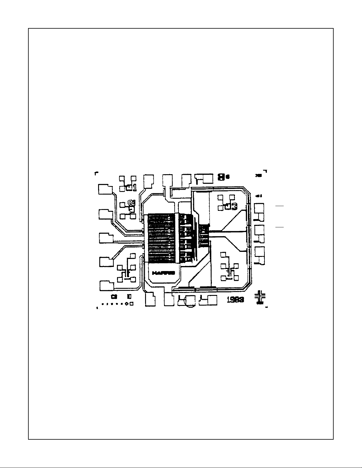
Metallization Topology
DIE DIMENSIONS:
76 mils x 63 mils x 14 mils ±1 mil
METALLIZATION:
Type: AlSi
Thickness: 11k
Å ±2kÅ
GLASSIVATION:
Type: SiO2
Thickness: 8k
Å ±1kÅ
Metallization Mask Layout
HS-54C138RH
HS-54C138RH
Y5 (10)
Y4 (11)
Y3 (12)
Y2 (13)
Y1 (14)
(9) Y6
Y0 (15)
(8) GND
VDD (16)
(7) Y7
A (1)
(6) G1
B (2)
(5)
(4)
(3) C
G2B
G2A
Spec Number 518053
4

HS-54C138RH
Typical applications include systems which require multiple
input/output ports and memories. When the HS-54C138RH
is enabled one of the eight outputs will go low. This output
can be used to select a particular device or a group of
devices. The HS-54C138RH can also be cascaded to
provide an enabling scheme for larger systems and allow
one decoder to control eight other decoders as in Figure 1.
SELECT B
TO OTHER
DEVICES
HS-54C138RH
Y7 Y6 Y5 Y4 Y3 Y2 Y1 Y0
Y7 Y6 Y5 Y4 Y3 Y2 Y1 Y0
Figure 2 shows a configuration that can be used to enable
multiple I/O ports or memory devices. Up to 24 memory
devices or I/O ports can be controlled using this circuit.
For demultiplexer operation, one of the three enable inputs is
used as the data input while the other two inputs are enable.
The transmitted data is distributed to the proper output as
determined by the 3-line select inputs. See Figure 3.
SELECT A ENABLE
HS-54C138RH
Y7 Y6 Y5 Y4 Y3 Y2 Y1 Y0
“0”“1”“0”“1”“0”“1”
ENABLEENABLEENABLE
HS-54C138RH
HS-54C138RH
Y7 Y6 Y5 Y4 Y3 Y2 Y1 Y0
FIGURE 1
EN EN EN A4 A3 A2 A1 A0
G1 G2B G2A C B A
Y7 Y6 Y5 Y4 Y3 Y2 Y1 Y0
G1 G2B G2A C B A
Y7 Y6 Y5 Y4 Y3 Y2 Y1 Y0
PORT NUMBERS OR CHIP SELECTS
G1 G2B G2A C B A
Y7 Y6 Y5 Y4 Y3 Y2 Y1 Y0
FIGURE 2
DAT A
INPUT
EN EN
SELECT
G1 G2B G2A C B A
Y7 Y6 Y5 Y4 Y3 Y2 Y1 Y0
FIGURE 3
5
Spec Number 518053

HS-54C138RH
All Intersil semiconductor products are manufactured, assembled and tested under ISO9000 quality systems certification.
Intersil products are sold by description only. Intersil Cor poration reserves the right to make changes in circuit design and/or specifications at any time without
notice. Accordingly, the reader is cautioned to verify that data sheets are current before placing orders. Information furnished by Intersil is believed to be accurate
and reliable. However, no responsibility is assumed by Intersil or its subsidiaries for its use; nor for any infringements of patents or other rights of third parties which
may result from its use. No license is granted by implication or otherwise under an y patent or patent rights of Intersil or its subsidiaries.
For information regarding Intersil Corporation and its products, see web site http://www.intersil.com
Sales Office Headquarters
NORTH AMERICA
Intersil Corporation
P. O. Box 883, Mail Stop 53-204
Melbourne, FL 32902
TEL: (407) 724-7000
FAX: (407) 724-7240
EUROPE
Intersil SA
Mercure Center
100, Rue de la Fusee
1130 Brussels, Belgium
TEL: (32) 2.724.2111
FAX: (32) 2.724.22.05
ASIA
Intersil (Taiwan) Ltd.
Taiwan Limited
7F-6, No. 101 Fu Hsing North Road
Taipei, Taiwan
Republic of China
TEL: (886) 2 2716 9310
FAX: (886) 2 2715 3029
Spec Number
6
 Loading...