

Intersil Corporation HS-3530RH Datasheet
August 1995
HS-3530RH
Low Power, Radiation Hardened
Programmable Operational Amplifier
Features
• Radiation Environment
- Neutron Fluence (Φ) 5 x 10
- Gamma Rate 1 x 10
(γ)
- Gamma Dose (γ) 1 x 10
• Wide Range AC Programming
- Slew Rate 0.06 to 3V/µs
- Gain X Bandwidth 100kHz to 5.0MHz
• Wide Range DC Programming
- Power Supply Range ±3.0V to ±15V
• Supply Current 10µA to 1.2mA
• Dielectrically Isolated Device Islands
• Short Circuit Protection
12
n/cm2 (E ≥ 10KeV)
9
RAD (Si)/s
6
RAD (Si)
Description
The HS-3530RH is a Low Power Operational Amplifier which
is an internally compensated monolithic device offering a
wide range of performance specifications. Parameters such
as power dissipation, slew rate, bandwidth, noise and input
DC parameters are programmed by selecting an external
resistor or current source. Supply voltages as low as ±3V
may be used with little degradation of AC performance. The
HS-3530RH has been specifically designed to meet
exposure to space radiation environments. Operation from -55
o
to +125
C is guaranteed.
A major advantage of the HS-3530RH is that operating
characteristics remain virtually constant over a wide supply
range (±3V to ±15V), allowing the amplifier to offer maximum
performance in almost any system, including battery
operated equipment. A primary application for this device is
in active filtering and conditioning for a wide variety of
signals that differ in frequency and amplitude. Also, by
modulating the set current, it can be used for designs such
as current controlled oscillators/modulators, sample and
hold circuits and variable active filters.
o
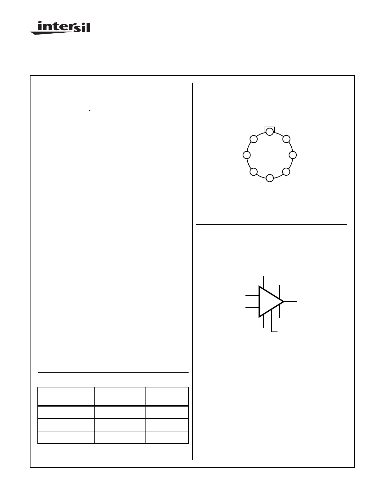
Pinout
8 LEAD METAL CAN PACKAGE (CAN)
OFFSET
NULL
INVERTING
INPUT
NON-INVERTING
NOTE:
1. Case tied to V-.
INPUT
Functional Diagram
C
-IN
+IN
MIL-STD-1835 MACY1-X8
TOP VIEW
ISET
8
1
2
3
4
V-
+V
OFFSET
NULL 2
7
2
3
1
4
-V
5
8
ISET
OFFSET
NULL 1
7
5
6
V+
6
OFFSET
NULL
OUTPUT
OUT
Ordering Information
TEMPERATURE
PART NUMBER
HS2-3530RH-8 -55oC to +125oC 8 Lead Metal Can
HS2-3530RH-Q -55oC to +125oC 8 Lead Metal Can
HS2-3530RH/SAMPLE +25oC 8 Lead Metal Can
CAUTION: These devices are sensitive to electrostatic discharge; follow proper IC Handling Procedures.
http://www.intersil.com or 407-727-9207
RANGE PACKAGE
| Copyright © Intersil Corporation 1999
762
Spec Number
518079
File Number 3024.2
DB NA
Specifications HS-3530RH
Absolute Maximum Ratings Reliability Information
Voltage Between V+ and V- Terminals. . . . . . . . . . . . . . . . . . . . 40V
Differential Input Voltage . . . . . . . . . . . . . . . . . . . . . . . . . . . . . . 20V
Voltage at Either Input Terminal . . . . . . . . . . . . . . . . . . . . . . V+ to V-
ISET (Current at ISET). . . . . . . . . . . . . . . . . . . . . . . . . . . . . . 500µA
VSET (Voltage to GND at ISET). . . . . . . . . (V+ -2.0V) < VSET < V+
Output Short Circuit Duration (Note 1) . . . . . . . . . . . . . . . . Indefinite
Junction Temperature (TJ) . . . . . . . . . . . . . . . . . . . . . . . . . . +175oC
Storage Temperature Range . . . . . . . . . . . . . . . . . -65oC to +150oC
ESD Rating. . . . . . . . . . . . . . . . . . . . . . . . . . . . . . . . . . . . . . <2000V
Lead Temperature (Soldering 10s). . . . . . . . . . . . . . . . . . . . . 275oC
CAUTION: Stresses above those listed in “Absolute Maximum Ratings” may cause permanent damage to the device. This is a stress only rating and operation
of the device at these or any other conditions above those indicated in the operational sections of this specification is not implied.
Operating Conditions
Operating Temperature Range. . . . . . . . . . . . . . . . -55oC to +125oC
Operating Supply Voltage. . . . . . . . . . . . . . . . . . . . . . . . . .±3V to ±15V
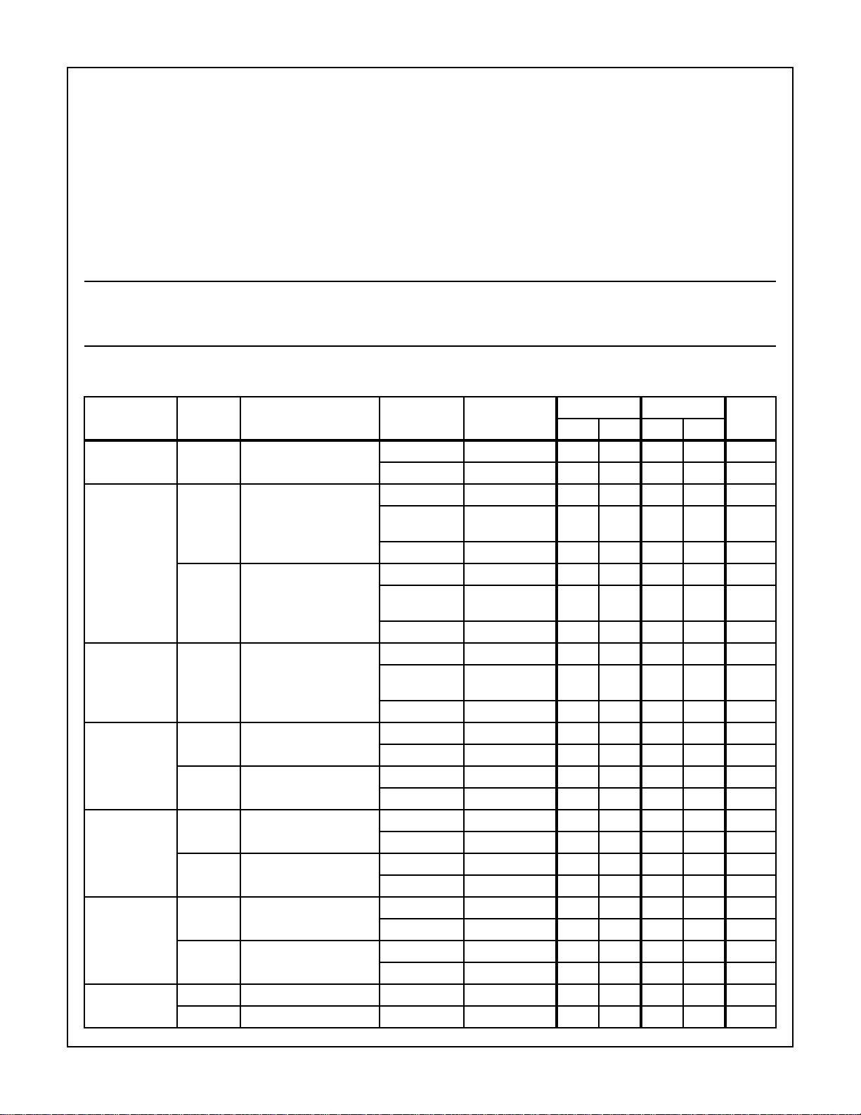
TABLE 1A. DC ELECTRICAL PERFORMANCE CHARACTERISTICS
Device Tested at: Supply Voltage = ±15V, RSOURCE = 100Ω, RLOAD = 500kΩ, VOUT = 0V, Unless Otherwise Specified.
Thermal Resistance θ
Metal Can Package. . . . . . . . . . . . . . . . . 160oC/W 70oC/W
Maximum Package Power Dissipation at +125oC Ambient:
Metal Can Package. . . . . . . . . . . . . . . . . . . . . . . . . . . . . . . 0.31W
If device power exceeds package dissipation capability, provide heat
sinking or derate linearly at the following rate:
Metal Can Package. . . . . . . . . . . . . . . . . . . . . . . . . . . .6.3mW/oC
VINcm ≤1/2 (V+ - V-)
RL ≥ 2kV
JA
θ
JC
GROUP A
PARAMETER SYMBOL CONDITIONS
Input Offset
Voltage
Input Bias
Current
Input Offset
Current
Large Signal
Voltage Gain
Common Mode
Rejection Ratio
Output Voltage
Swing
Output Current +IOUT RL = 2kΩ 1 +25oC 0.25 - 2.5 - mA
VIO VCM = 0V 1 +25oC -3 3 -3 3 mV
+IB VCM = 0V, +RS = 10kΩ
-RS = 100Ω
Note 2
-IB VCM = 0V, +RS = 100Ω
-RS = 10kΩ
Note 2
IIO VCM = 0V, +RS = 10kΩ
-RS = 10kΩ
Note 2
+AVOL VOUT = 0V and +10V
Note 1
-AVOL VOUT = 0V and -10V
Note 1
+CMRR ∆VCM = +5V, +V = +10V
-V = -20V, VOUT = -5V
-CMRR ∆VCM = -5V, +V = +20V
-V = -10V, VOUT = +5V
+VOUT Note 1 1 +25oC 12.5 - 12.5 - V
-VOUT Note 1 1 +25oC - -12.5 - -12.5 V
-IOUT RL = 2kΩ 1 +25oC - -0.25 - -2.5 mA
SUBGROUP TEMPERATURE
2, 3 +125oC, -55oC -5 5 -5 5 mV
1 +25oC - - -40 40 nA
2, 3 +125oC, 0oC - - -50 +50 nA
3 -55oC - - -60 60 nA
1 +25oC - - -40 40 nA
2, 3 +125oC, 0oC - - -50 +50 nA
3 -55oC - - -60 60 nA
1 +25oC - - -15 15 nA
2, 3 +125oC, 0oC - - -20 +20 nA
3 -55oC - - -30 30 nA
4 +25oC 65 - 80 - kV/V
5, 6 +125oC, -55oC 25 - 50 - kV/V
4 +25oC 65 - 80 - kV/V
5, 6 +125oC, -55oC 25 - 50 - kV/V
1 +25oC 80 - 80 - dB
2, 3 +125oC, -55oC 80 - 80 - dB
1 +25oC 80 - 80 - dB
2, 3 +125oC, -55oC 80 - 80 - dB
2, 3 +125oC, -55oC 10.5 - 10.5 - V
2, 3 +125oC, -55oC - -10.5 - -10.5 V
ISET = 1.5µA ISET = 15µA
UNITSMIN MAX MIN MAX
763
Spec Number 518079
Specifications HS-3530RH
TABLE 1A. DC ELECTRICAL PERFORMANCE CHARACTERISTICS (Continued)
Device Tested at: Supply Voltage = ±15V, RSOURCE = 100Ω, RLOAD = 500kΩ, VOUT = 0V, Unless Otherwise Specified.
GROUP A
PARAMETER SYMBOL CONDITIONS
Quiescent Power
Supply Current
Power Supply
Rejection Ratio
NOTES:
1. RL = 75kΩ at ISET = 1.5µA, RL = 5kΩ at ISET = 15µA.
2. Temperature 0oC performed for Intersil -8 product flow only.
Device Tested at: Supply Voltage = ±3V, RSOURCE = 100Ω, RLOAD = 500kΩ, VOUT = 0V, Unless Otherwise Specified.
PARAMETER SYMBOL CONDITIONS
Input Offset
Voltage
Large Signal
Voltage Gain
Common Mode
Rejection Ratio
Output Voltage
Swing
Quiescent Power
Supply Current
Power Supply
Rejection Ratio
NOTE:
1. RL = 75kΩ at ISET = 1.5µA, RL = 5kΩ at ISET = 15µA.
+ICC IOUT = 0mA 1 +25oC - 15 - 150 µA
-ICC IOUT = 0mA 1 +25oC -15 - -150 - µA
+PSRR ∆VSUP = 10V
+V = +10V, -V = -15V
+V = +20V, -V = -15V
-PSRR ∆VSUP = 10V
+V = +15V, -V = -10V
+V = +15V, -V = -20V
TABLE 1B. DC ELECTRICAL PERFORMANCE CHARACTERISTICS
VIO VCM = 0V 1 +25oC -3 3 -3 3 mV
+AVOL VOUT = 0V and +1V
Note 1
-AVOL VOUT = 0V and -1V
Note 1
+CMRR ∆VCM = +1.5V
+V = +1.5V, -V = -4.5V
VOUT = -1.5V
-CMRR ∆VCM = -1.5V
+V = +4.5V, -V = -1.5V
VOUT = +1.5V
+VOUT Note 1 1 +25oC 2.0 - 2.0 - V
-VOUT Note 1 1 +25oC - -2.0 - -2.0 V
+ICC IOUT = 0mA 1 +25oC - 15 - 150 µA
-ICC IOUT = 0mA 1 +25oC -15 - -150 - µA
+PSRR ∆VSUP = 1.5V
+V = +3V, -V = -3V
+V = +4.5V, -V = -3V
-PSRR ∆VSUP = 1.5V
+V = +3V, -V = -3V
+V = +3V, -V = -4.5V
SUBGROUP TEMPERATURE
2, 3 +125oC, -55oC - 15 - 160 µA
2, 3 +125oC, -55oC -15 - -160 - µA
1 +25oC 80 - 80 - dB
2, 3 +125oC, -55oC 80 - 80 - dB
1 +25oC 80 - 80 - dB
2, 3 +125oC, -55oC 80 - 80 - dB
GROUP A
SUBGROUP TEMPERATURE
2, 3 +125oC, -55oC -5 5 -5 5 mV
4 +25oC 25 - 25 - kV/V
5, 6 +125oC, -55oC 15 - 25 - kV/V
4 +25oC 25 - 25 - kV/V
5, 6 +125oC, -55oC 15 - 25 - kV/V
1 +25oC 80 - 80 - dB
2, 3 +125oC, -55oC 80 - 80 - dB
1 +25oC 80 - 80 - dB
2, 3 +125oC, -55oC 80 - 80 - dB
2, 3 +125oC, -55oC 2.0 - 2.0 - V
2, 3 +125oC, -55oC - -2.0 - -2.0 V
2, 3 +125oC, -55oC - 15 - 160 µA
2, 3 +125oC, -55oC -15 - -160 - µA
1 +25oC 80 - 80 - dB
2, 3 +125oC, -55oC 80 - 80 - dB
1 +25oC 80 - 80 - dB
2, 3 +125oC, -55oC 80 - 80 - dB
ISET = 1.5µA ISET = 15µA
ISET = 1.5µA ISET = 15µA
UNITSMIN MAX MIN MAX
UNITSMIN MAX MIN MAX
764
Spec Number 518079

Specifications HS-3530RH
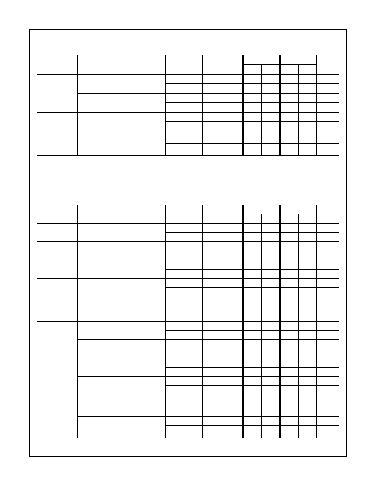
TABLE 2. AC ELECTRICAL PERFORMANCE CHARACTERISTICS
Device Tested at: CL = 100pF, AVCL = +1, RL = 75kΩ, Unless Otherwise Specified.
GROUP A
PARAMETER SYMBOL CONDITIONS
VSUPPLY = ±15V
Slew Rate
Note 1
Rise & Fall Time TR VOUT = 0 to +400mV
Overshoot +OS VOUT = 0 to +400mV 9 +25oC-35-35%
VSUPPLY = ±3V
Slew Rate
Note 1
Device Characterized at: RSOURCE = 50Ω, CL = 100pF, AVCL = +1, Unless Otherwise Specified.
PARAMETER SYMBOL CONDITIONS NOTES TEMPERATURE
VSUPPLY = ±15V
Differential Input
Resistance
Full Power Bandwidth FPBW VPEAK = 10V 1, 2 +25oC 0.4 - 4 - kHz
Minimum Closed
Loop Stable Gain
Output Resistance ROUT Open Loop 1 +25oC - 10 - 10 Ω
Quiescent Power
Consumption
Output Short-Circuit
Current
Gain Bandwidth
Product
VSUPPLY = ±3V
Gain Bandwidth
Product
NOTES:
1. Parameters listed in Table 3 are controlled via design or process parameters and are not directly tested at final production. These parameters are lab characterized upon initial design release, or upon design changes. These parameters are guaranteed by characterization
based upon data from multiple production runs which reflect lot to lot and within lot variation.
2. Full Power Bandwidth guarantee based on Slew Rate measurement using FPBW = Slew Rate/(2πVPEAK).
3. Quiescent Power Consumption based upon Quiescent Supply Current test maximum. (No load on outputs).
4. Caution: Continuous long-duration short-circuit operation may degrade the operating life of the device.
+SR VOUT = -10V to +10V 9 +25oC 0.025 - 0.25 - V/µs
-SR VOUT = +10V to -10V 9 +25oC 0.025 - 0.25 - V/µs
10% < TR < 90%
TF VOUT = 0 to -400mV
10% < TF < 90%
-OS VOUT = 0 to -400mV 9 +25oC-35-35%
+SR VOUT = -2V to +2V 9 +25oC 0.01 - 0.1 - V/µs
-SR VOUT = +2V to -2V 9 +25oC 0.01 - 0.1 - V/µs
TABLE 3. AC ELECTRICAL PERFORMANCE CHARACTERISTICS
RIN VCM = 0V 1 +25oC50-50-MΩ
CLSG RL = 2kΩ, CL = 50pF 1 -55oC to +125oC +1 - +1 - V/V
PC VOUT = 0V, IOUT = 0mA 1, 3 -55oC to +125oC - 4.8 - 4.8 mW
IOSC VOUT = 0V 1, 4 +25oC -14 38 -27 42 mA
GBWP AVCL = 10V/V
VO = 200mV, fO = 10kHz
GBWP AVCL = 10V/V
VO = 200mV, fO = 10kHz
SUBGROUP TEMPERATURE
9 +25oC - 8.0 - 0.8 µs
9 +25oC - 8.0 - 0.8 µs
1 +25oC 45 - 750 - kHz
1 +25oC 30 - 600 - kHz
ISET = 1.5µA ISET = 15µA
UNITSMIN MAX MIN MAX
ISET = 1.5µA ISET = 15µA
UNITSMIN MAX MIN MAX
765
Spec Number 518079
 Loading...