Intersil Corporation HS-3530ARH Datasheet

HS-3530ARH
Data Sheet March 1999
Radiation Hardened Programmable Low
Power Op Amp
The HS-3530ARH is a Low Power Operational Amplifier
which is an internally compensated monolithic device
offering a wide range of performance specifications.
Parameterssuch as powerdissipation, slewrate, bandwidth,
noise and input DC parameters are programmed by
selecting an external resistor or current source. Supply
voltagesas low as ±3V maybe used with little degradation of
AC performance. The HS-3530ARH has been specifically
designed to meet exposure to space r adiation environments .
Operation from -55
A major advantage of the HS-3530ARH is that operating
characteristics remain virtually constant over a wide supply
range (±3V to ±15V), allowingthe amplifier to offer maximum
performance in almost any system, including battery
operated equipment. A primary application for this device is
in active filtering and conditioning for a wide variety of
signals that differ in frequency and amplitude. Also, by
modulating the set current, it can be used for designs such
as current controlled oscillators/modulators, sample and
hold circuits and variable active filters.
o
C to 125oC is guaranteed.
File Number 4653
Features
• Radiation Performance
- Gamma Dose . . . . . . . . . . . . . . . . . . . . 3 x 10
- SEL. . . . . . . . . . . . . . . . . . . Immune (RSG DI Process)
• Wide Range AC Programming
- Slew Rate . . . . . . . . . . . . . . . . . . . . . . 0.025 to 0.1V/µs
- Gain X Bandwidth. . . . . . . . . . . . . . . . 30kHz to 750kHz
• Wide Range DC Programming
- Power Supply Range . . . . . . . . . . . . . . . ±3.0V to ±15V
• Supply Current . . . . . . . . . . . . . . . . . . . . . .15µA to 150µA
• Output Current . . . . . . . . . . . . . . . . . . . .0.25mA to 2.5mA
• Quiescent Power . . . . . . . . . . . . . . . . . . . . . 4.8mW (Max)
• Dielectrically Isolated Device Islands
• Short Circuit Protection
• Full -55
o
C to 125oC Military Temperature Range
5
RAD(Si)
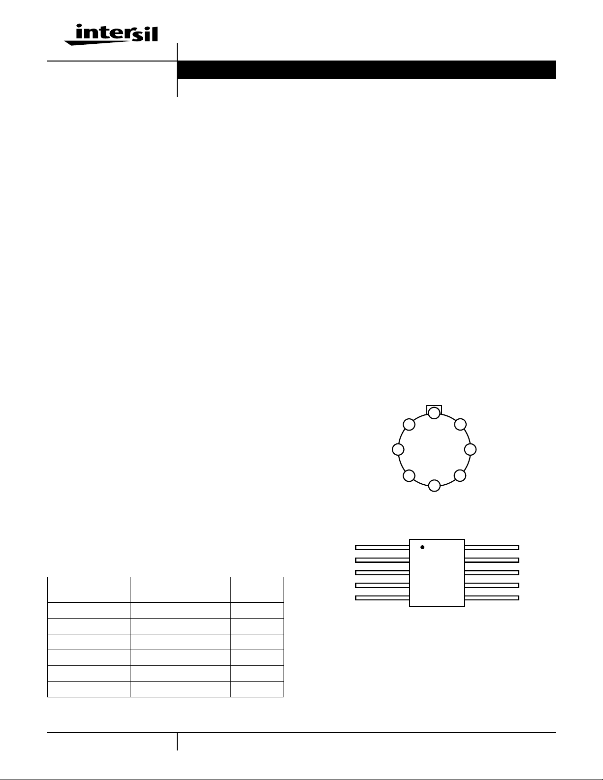
Pinouts
HS2-3530ARH (CAN), MACY1-X8
TOP VIEW
Specifications
Specifications for Rad Hard QML devices are controlled by
the Defense Supply Center in Columbus (DSCC). The SMD
numbers listed below must be used when ordering.
Detailed Electrical Specifications for the HS-3530ARH
are contained in SMD 5962-95687. A “hot-link” to the
DSCC website is provided on our homepage for
downloading the document.
www.intersil.com/spacedefense/ne wsafc lasst.asp
The Intersil Quality Management Plan, listing all screening
operations, is available on our website.
www.intersil.com/quality/manuals.asp
Ordering Information
ORDERING
NUMBER
5962F9568701QGA HS2-3530ARH-8 -55 to 125
5962F9568701VGA HS2-3530ARH-Q -55 to 125
5962F9568701VXC HS9-3530ARH-Q -55 to 125
5962F9568701V9A HS0-3530ARH-Q -55 to 125
NA HS2-3530ARH/Proto -55 to 125
NA HS9-3530ARH/Proto -55 to 125
PART
NUMBER
TEMP.
RANGE (oC)
NON-INVERTING
OFFSET
- IN
+ IN
V -
I
SET
OFFSET
NULL
INVERTING
HS9-3530ARH (FLATPACK), CDFP3-F10
INPUT
INPUT
2
1
3
TOP VIEW
1NC
2
3
4
5
8
7
V+
OUTPUT
6
OFFSET
5
4
V-
NULL
10
9
8
7
6
I
SET
V +
OUTPUT
OFFSET
NC
1
CAUTION: These devices are sensitive to electrostatic discharge; follow proper IC Handling Procedures.
1-888-INTERSIL or 321-724-7143 | Copyright © Intersil Corporation 1999

HS-3530ARH
Die Characteristics
DIE DIMENSIONS:
1720µm x 1390µm x 533µm ±25.4µm
(68 mils x 55 mils x 21 mils ±1 mil)
INTERFACE MATERIALS
GLASSIVATION
Type: Silox (SiO
Thickness: 8.0kA ±1.0kA
TOP METALLIZATION
Type: AlSiCu
Thickness: 16.0kA ±2kA
)
2
SUBSTRATE:
Radiation Hardened Silicon Gate,
Dielectric Isolation
BACKSIDE FINISH:
Silicon
ASSEMBLY RELATED INFORMATION
SUBSTRATE POTENTIAL:
Unbiased (DI)
ADDITIONAL INFORMATION
WORST CASE CURRENT DENSITY:
5
<2.0 x 10
A/cm
TRANSISTOR COUNT:
49
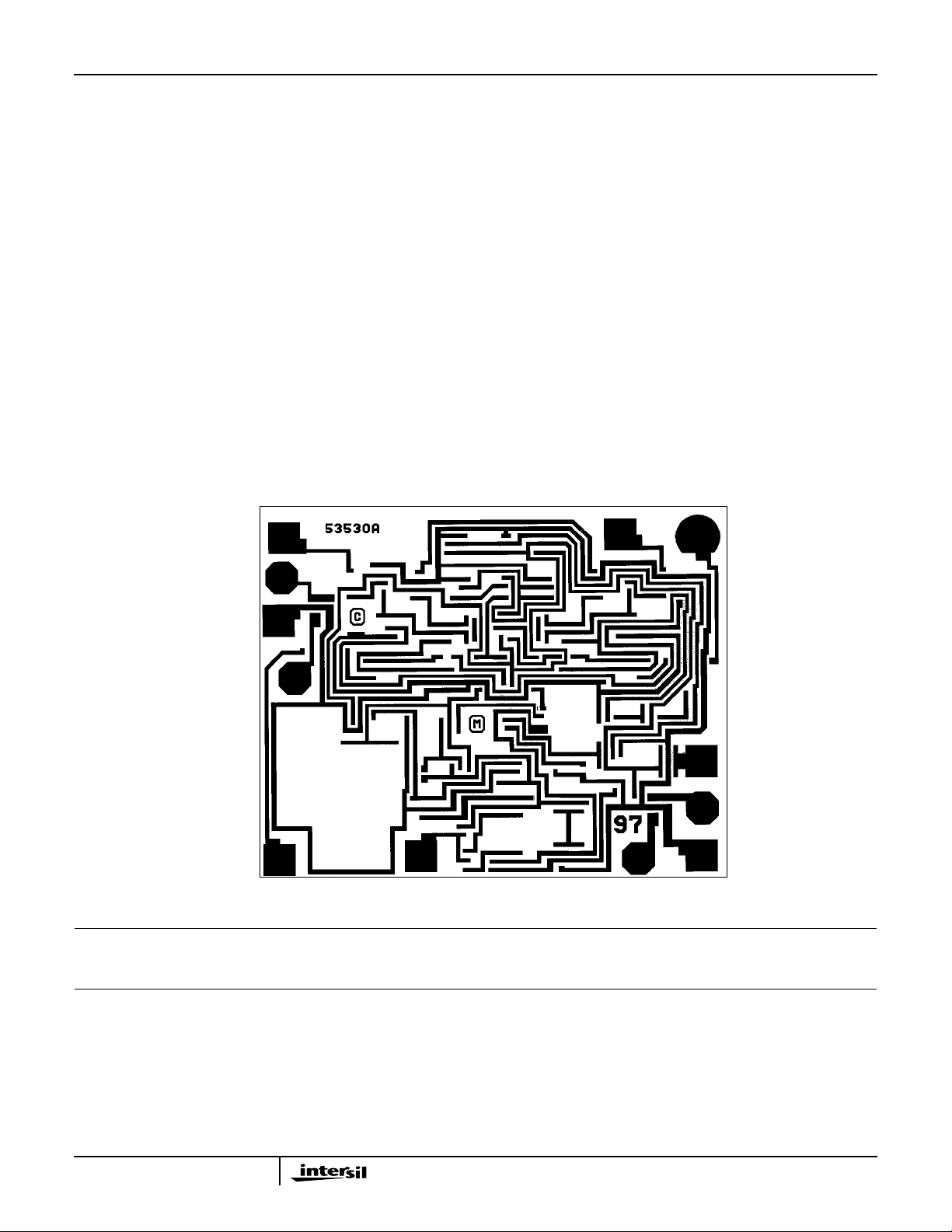
Metallization Mask Layout Pin Numbers shown are for the Can Package
HS-3530ARH
IN+
(3)
IN(2)
2
OFFSET
(1)
NC
V- (4)
NC
I
SET
(8)
NC
OFFSET (5)
V+ (7)NCOUTPUT (6)
All Intersil semiconductor products are manufactured, assembled and tested under ISO9000 quality systems certification.
Intersil semiconductor products are sold by description only.Intersil Corporation reserves the right to make changes in circuit design and/or specifications at any time without notice. Accordingly, the reader is cautioned to verify that data sheets are current before placing orders. Information furnished by Intersil is believed to be accurate and
reliable. However, no responsibility is assumed by Intersil or its subsidiaries for its use; nor for any infringements of patents or other rights of third parties which may result
from its use. No license is granted by implication or otherwise under any patent or patent rights of Intersil or its subsidiaries.
For information regarding Intersil Corporation and its products, see web site www.intersil.com
Sales Office Headquarters
NORTH AMERICA
Intersil Corporation
P. O. Box 883, Mail Stop 53-204
Melbourne, FL 32902
TEL: (321) 724-7000
FAX: (321) 724-7240
EUROPE
Intersil SA
Mercure Center
100, Rue de la Fusee
1130 Brussels, Belgium
TEL: (32) 2.724.2111
FAX: (32) 2.724.22.05
ASIA
Intersil (Taiwan) Ltd.
7F-6, No. 101 Fu Hsing North Road
Taipei, Taiwan
Republic of China
TEL: (886) 2 2716 9310
FAX: (886) 2 2715 3029
2
 Loading...