

TM
www.BDTIC.com/Intersil
REFERENCE AN400
March 1997
HS-3282
CMOS ARINC Bus Interface Circuit
Features
• ARlNC Specification 429 Compatible
• Data Rates of 100 Kilobits or 12.5 Kilobits
• Separate Receiver and Transmitter Section
• Dual and Independent Receivers, Connecting Directly
to ARINC Bus
• Serial to Parallel Receiver Data Conversion
• Parallel to Serial Transmitter Data Conversion
• Word Lengths of 25 or 32 Bits
• Parity Status of Received Data
• Generate Parity of Transmitter Data
• Automatic Word Gap Timer
• Single 5V Supply
• Low Power Dissipation
• Full Military Temperat ure Range
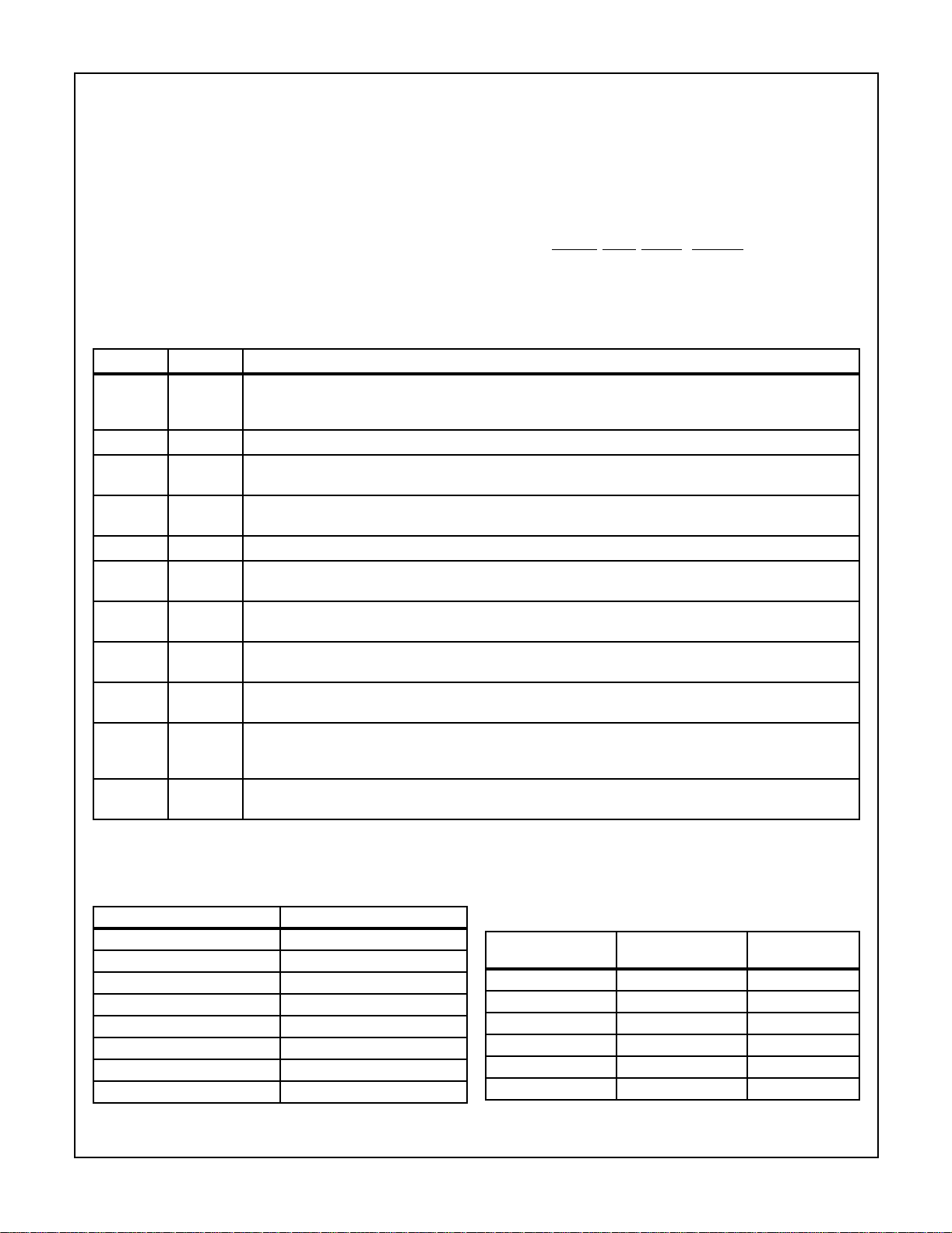
Ordering Information
PKG.
PACKAGE TEMP. RANGE PART NUMBER
o
CERDIP -55
SMD# 5962-8688001QA F40.6
CLCC -40
SMD# 5962-8688001XA J44.A
C to +125oC HS1-3282-8 F40.6
o
C to +85oC HS4-3282-9+ J44.A
o
C to +125oC HS4-3282-8 J44.A
-55
NO.
Description
The HS-3282 is a high performance CMOS bus interface
circuit that is intended to meet the requirements of ARINC
Specification 429, and similar encoded, time multiplexed
serial data protocols. This device is intended to be used with
the HS-3182, a monolithic Dl bipolar differential line driver
designed to meet the specifications of ARINC 429. The
ARINC 429 bus interface circuit cons ists of two (2) receivers
and a transmitter operating independently as shown in
Figure 1. The two receivers operate at a frequency that is
ten (10) times the receiver data rate, which can be the same
or different from the transmitter data rate. Although the two
receivers operate at the same frequency, they are
functionally independent and each receive s serial data asynchronously. The transmitter section of the ARINC bus
interfa ce circ uit consis ts m ainly of a First -In Fi rst- Ou t (FIFO )
memory and tim ing circuit. The FIFO memory is used to hold
up to eight (8) ARINC data words for transmission serially.
The timing circuit is used to correctly separate each ARINC
word as required by ARINC Specification 429. Even though
ARINC Specification 429 specifies a 32-bit word, including
parity, the HS-3282 can be programm ed to also operate with
a word length of 25 bits. The incoming receiver data word
parity is checked, and a parity status is stor ed in the receiver
latch and output on Pin BD08 during the 1st word. [A logic
“0” indicates that an odd number of logic “1” s were received
and stored; a l ogic “1” indicat es that an even number of l ogic
“1”s were received and stored]. In the transmitter the parity
generator will generate either odd or even parity depending
upon the status of PARCK control signal. A logic “0” on
BD12 will cause odd parity to be used in the output data
stream.
Versatility is provided in both the transmitter and receiver by
the external clock input which allows the bus interface circuit
to operate at data rates from 0 to 100 kilobits. The external
clock must be ten (10) times the data rate to insure no data
ambiguity.
The ARINC bus interface circuit is fully guaranteed to
support the data rates of ARINC specification 429 over both
the voltage (±5%) and full military temperature range. It
interfaces with UL, CMOS or NMOS support circuitry, and
uses the standard 5-volt V
CAUTION: The se devices are s ensitive to electrostatic di schar ge; foll ow proper IC Handling Proced ures.
1-888-INTERSIL or 321-724-7143
Copyright © Intersil Americas Inc. 2002. All Rights Reserved
| Intersil (and design) is a trademark of Intersil Americas Inc.
183
CC
supply.
FN2964.2
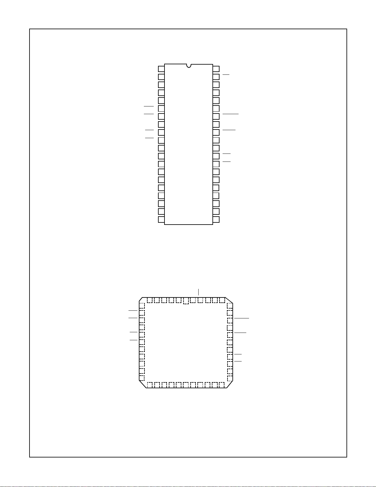
Pinouts
www.BDTIC.com/Intersil
V
DD
429DI1(A)
429DI1(B)
429DI2(A)
429DI2(B)
D/R1
D/R2
SEL
EN1
EN2
BD15
BD14
BD13
BD12
BD11
BD10
BD09
BD08
BD07
BD06
HS-3282
HS-3282 (CERDIP)
TOP VIEW
1
2
3
4
5
6
7
8
9
10
11
12
13
14
15
16
17
18
19
20
40
39
38
37
36
35
34
33
32
31
30
29
28
27
26
25
24
23
22
21
NC
MR
TX CLK
CLK
NC
NC
CWSTR
ENTX
429D0
429D0
TX/R
PL2
PL1
BD00
BD01
BD02
BD03
BD04
BD05
GND
NC
D/R1
D/R2
SEL
EN1
EN2
BD15
BD14
BD13
BD12
BD11
HS-3282 (CLCC)
TOP VIEW
DD
429DI1(A)
429DI1(B)
429DI2(A)
NC
429DI2(B)
7
8
9
10
11
12
13
14
15
16
17
NC
BD10
46 3
BD09
25
BD08
BD07
MR
V
NC
TXCLK
CLK
44
1
GND
BD06
BD05
NC
40414243
39
NC
38
NC
37
CWSTR
ENTX
36
429D0
35
429D0
34
TX/R
33
PL2
32
PL1
31
BD00
30
BD01
29
2827262524232221201918
BD04
BD03
BD02
184
HS-3282
www.BDTIC.com/Intersil
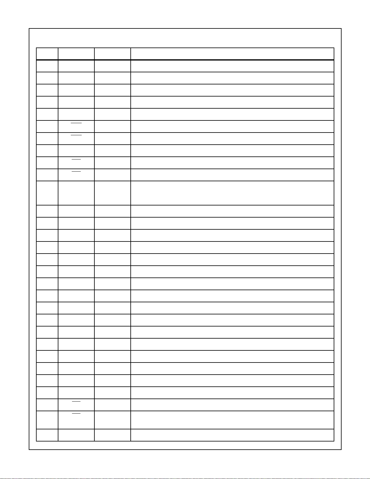
Pin Description
PIN SYMBOL SECTION DESCRIPTION
1V
2 429 DI1 (A) Receiver ARlNC 429 data input to Receiver 1.
3 429 DI1 (B) Receiver ARlNC 429 data input to Receiver 1.
4 429 Dl2 (A) Re ce iv er ARINC 42 9 data inpu t to Rece iv er 2.
5 429 DI2 (B) Receiv er ARINC 42 9 da t a in pu t to Receiver 2.
6D/R1
7D/R2
8 SEL Receiver Bus Data Selector - Input signal to select one of two 16-bit words from either Receiver 1 or 2.
9EN1
10 EN2
11 BD15 Recs/Trans Bi-directional data bus for fetching dat a from either of the Receivers, or for loading data in to
12 BD14 Recs/Trans See Pin 11.
13 BD13 Recs/Trans See Pin 11.
14 BD12 Recs/Trans See Pin 11.
CC
Recs/Trans Supply pin 5 volts ±5%.
Receiver Device ready flag output from Receiver 1 indicating a valid data word is ready to be fetched.
Receiver Device ready flag output from Receiver 2 indicating a valid data word is ready to be fetched.
Receiver Input signal to enable data from Receiver 1 onto the data bus.
Receiver Input signal to enable data from Receiver 2 onto the data bus.
the Transmitter memo ry o r con trol word re gister. Se e Contro l W ord T able f or descripti on o f
Control Word bits.
15 BD11 Recs/Trans See Pin 11.
16 BD10 Recs/Trans See Pin 11.
17 BD09 Recs/Trans See Pin 11.
18 BD08 Recs/Trans See Pin 11.
19 BD07 Recs/Trans See Pin 11.
20 BD06 Recs/Trans See Pin 11.
21 GND Recs/T rans Circuit Gr ound.
22 BD05 Recs/Trans See Pin 11.
23 BD04 Recs/Tr ans See Pin 11. Control Word function not applicable.
24 BD03 Recs/Tr ans See Pin 11. Control Word function not applicable.
25 BD02 Recs/Tr ans See Pin 11. Control Word function not applicable.
26 BD01 Recs/Tr ans See Pin 11. Control Word function not applicable.
27 BD00 Recs/Tr ans See Pin 11. Control Word function not applicable.
28 PL1
29 PL2
Transmitter Paralle l load input signal loading the first 16-bit word into the T ransmitter memory.
Transmitter Parallel load input signal loading the first 16-bit word into the Transmitter memory and ini-
tiates data transfer into the memory stack.
30 TX/R Transmitter Transmit ter flag output to indicate the memory is empty.
185
HS-3282
www.BDTIC.com/Intersil
Pin Description (Continued)
PIN SYMBOL SECTION DESCRIPTION
31 429D0 Transmitter Data output from Transmitter
32 429D0
33 ENTX Transmitter Transmitter Enable input signal to initiate data transmission from FIFO memory.
34 CWSTR
35 - - No co nn ec tion. Mu st be lef t op en .
36 - - No connection. Must be left open or tied low but never tied high.
37 CLK Recs/Trans External clock input. May be either ten (10) or eighty (80) times the data rate. If using both
38 TXCLK Transmitter Transmitter Clock output. Delivers a clock frequency equal to the transmitter data rate.
39 MR
40 - - No Connection.
Transmitter Data output from Transmitter.
Recs/Trans Control word input strobe signal to latch the control word from the databus into the control
word register.
ARINC data rates it must be ten (10) times the highest data rate, (typically 1MHz).
Recs/Trans Master Reset. Active low pulse used to reset FIFO, bit counters, gap timer, word count signal,
TX/R an d various other flags and contr ols. Master reset does not reset t he control word
register. Usually only used on Power-Up or System Reset.
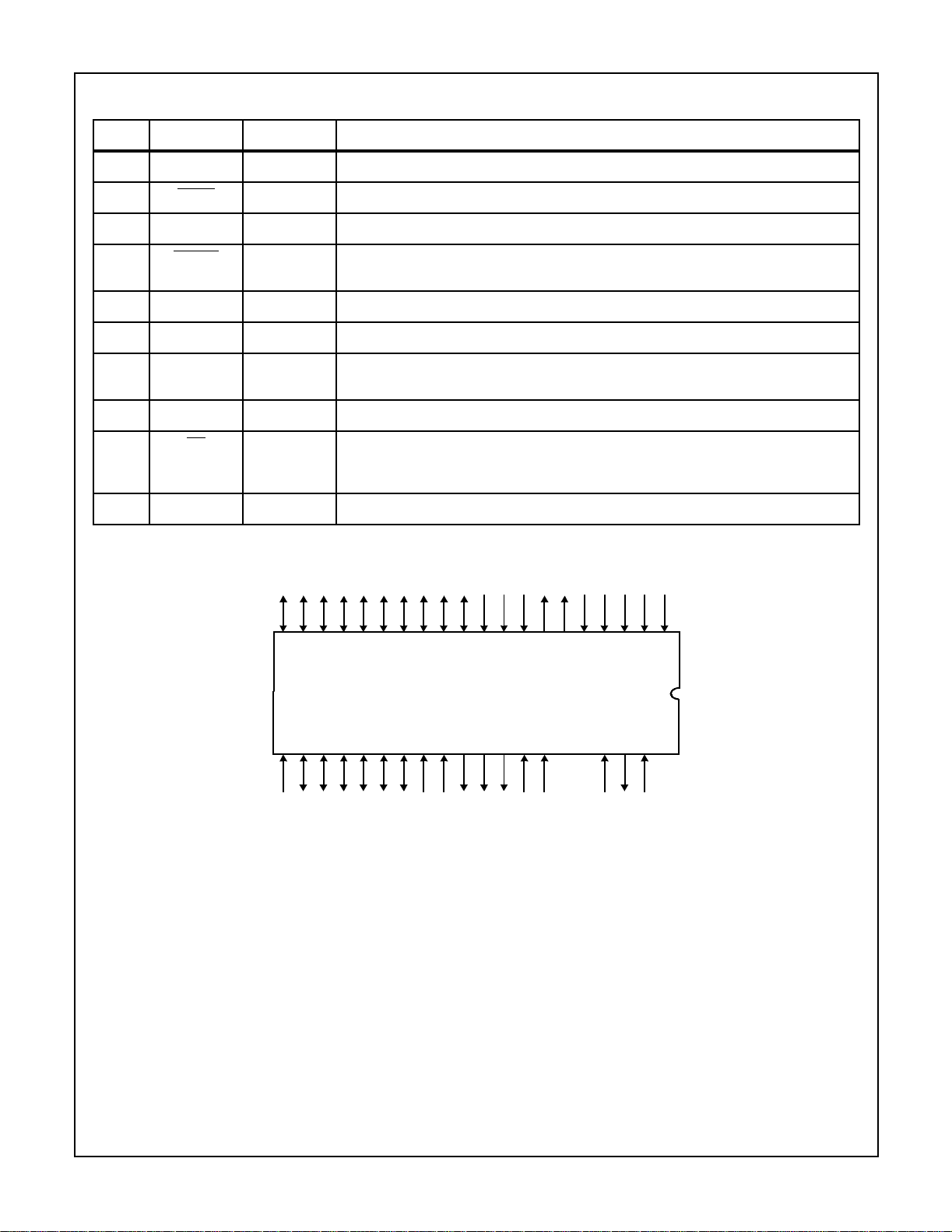
Pinout
13 12345678910111214151617181920
28 40393837363534333231302927262524232221
NCNC NC
186
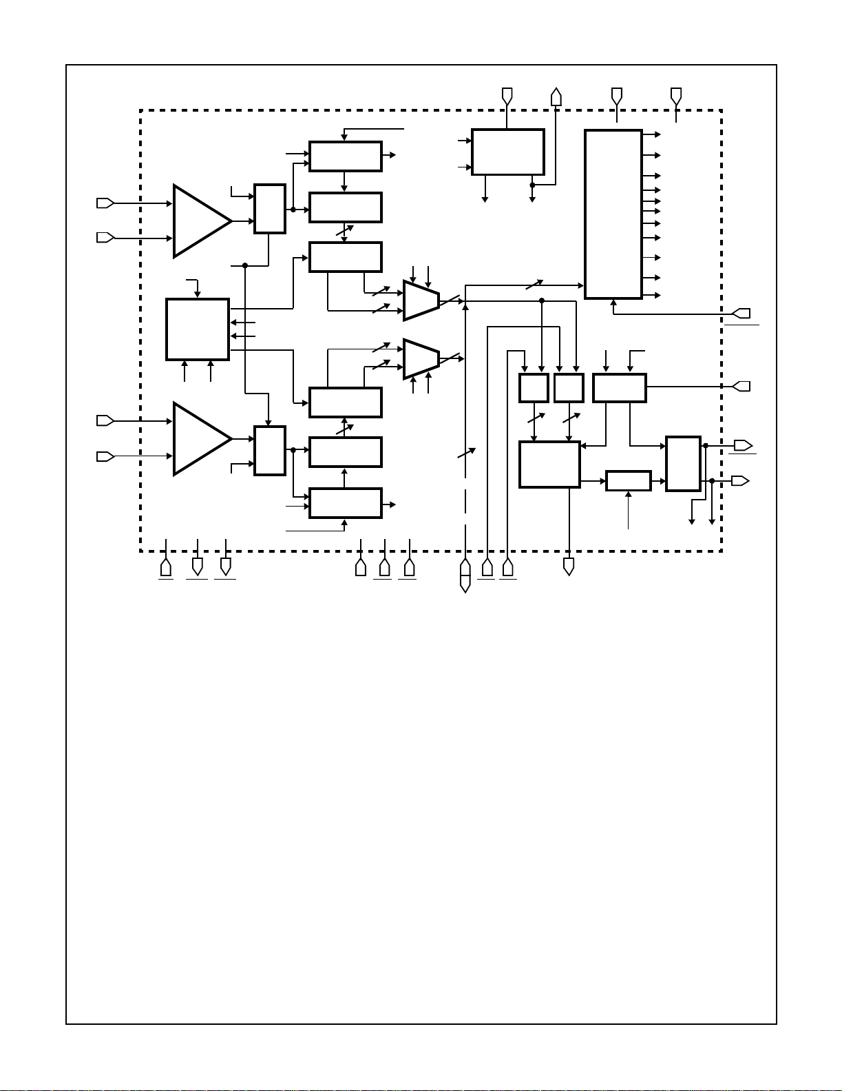
Operational Description
www.BDTIC.com/Intersil
HS-3282
The HS-3282 is designed to support ARINC Specification
429 and other serial data protocols that use a similar format
by collecting the receiving, transmitting, synchronizing,
timing and parity fu nctions on a single, low power LSl circui t.
It goes beyond the ARlNC requirements by providing for
either odd or even parity, and giving the user a choice of
either 25 or 32-bit word le ngths. The rece iver and transmit ter
sections operate independently of each other. The serial-toparallel conversion required of the receiver and the parallelto-serial conversion requirements of the transmitter have
been incorporated into the bus interface circuit.
Provisions have been made through the external clock input
to provide dat a rate flexibi li ty. This requires an external clock
that is 10 times the data rate.
To obtain the flexibility discussed above, a number of
external control signals are required, To reduce the pin
count requirements, an internal contr ol word register is used.
The control word is latched from the data bus into the register by the Control
Word Strobe (CWSTR) signal going to a
logic “1”. Eleven (11) control functions are used, and along
with the Bus Data (BD) line are list ed below:
Control Word
PIN NAME SYMBOL FUNCTION
BD05 SLFTST Conne cts the se lf test si gnal from t he transmi tter dire ctly to th e receiver shift reg isters, bypassin g the input
recei vers . Rec eiv er 1 r ece ives Dat a True an d Rec eive r 2 re cei ves Da ta Not . Not e tha t th e tran smit ter out put
remains active. (Logic “0” on SLFTST Enables Self Test).
BD06 SDENB1 Signal to Activate the Source/Destination (S/D) Decoder for Receiver 1. (Logic “1” activates S/D Decoder).
BD07 X1 If SDENB1 = “1” then this bit is compared with ARlNC Data Bit #9. If Y1 also matches (see Y1), the word will be
BD08 Y1 If SDENBI = “ 1” then th is bit is co mpa red with ARIN C Da ta B it # 10 . If X1 also matc he s (se e X1 ), th e wor d wil l
BD09 SDENB2 Signal to activate the Source/Destination (S/D) Decoder for Receiver 2. (Logic “1” activates S/D Decoder).
BD10 X2 If SDENB2 = “1” then this bit is compared with ARlNC Data Bit #9. If Y2 also matches (see Y2), the word will be
BD11 Y2 If SDENB2 = “1” then this bit is compared with ARINC Data Bit #10. If X2 also matches (see X2), the word will
BD12 PARCK Signal us ed to inv ert the t ran smi t ter pa rit y bi t fo r te st of pa ri ty ci r cu its. Lo gic “ 0” se le ct s n orma l o dd par i ty. Log ic
BD13 TXSE L Selects hi gh o r low Tra nsm itter da ta rat e. I f TX SEL = “ 0” the n t ransm it ter da ta rate i s eq ua l to th e cl ock rat e
BD14 RCVSEL Selects high or low Receiver data rate. If RCVSEL = “0” then the received data rate should be equal to the clock
BD15 WLSEL Selects word length. If WLSEL = “0” a 32-bit word format will be selected. If WLSEL = “1” a 25-Bit word format
accepted by the Receiver 1. If SDENB1 = “0” this bit becomes a don’t care.
be accepted by the Receiver 1. If SDENB1 = “0” this bit becomes a don’t care.
accepted by the Receiver 2. If SDENB2 = “0” this bit becomes a don’t care.
be accepted by the Receiver 2. If SDENB2 = “0” this bit becomes a don’t care.
“I” selects even parity.
divide d by ten (10). If TXSE L = “1” then transmitter data rate is equal to the clock rate divided by eighty (80).
rate divide d by te n (10), i f RCVSEL = “1 “t hen th e re ceived data ra te shou ld be e qual to the cl ock rate di vide d
by eighty (80).
will be selected.
ARlNC 429 DATA FORMAT as input to the Receiver and
output from the Transm itter is as follows:
TABLE 1. ARINC 429 32-BIT DATA FORMAT
ARINC BIT # FUNCTION
1 - 8 Label
9 - 10 SDl or Data
11 LSB
12 - 27 Data
28 MSB
29 Sign
30, 31 SSM
32 Parity S tatus
This format is shuffled when seen on the sixteen bidirectional input/outputs. The format shown below is used from
the receivers and input to the transmitter :
TABLE 2A. WORD 1 FORMAT
BI-DIRECTIONAL
BIT # FUNCTION ARINC BlT #
15, 14 Data 13, 12
13 LSB 11
12, 11 SDl or Data 10, 9
10, 9 SSM Status 31, 30
8 Parity Status 32
7 - 00 Label 1 - 8
187
HS-3282
www.BDTIC.com/Intersil
TABLE 2B. WORD 2 FORMAT
BI-DIRECTIONAL
BlT# FUNCTION ARINC BIT#
15 Sign 29
14 MSB 28
13 - 00 Data 27 - 14
Receiver Parity Statu s:
0 = Odd Parity
1 = Even Parity
If the receiver input data word string is broken before the
entire data word is received, the receiver will reset and
ignore the partially received data word.
If the transmitter is used to transmit consecutive data words,
each word wil l be separated by a four (4) bit “null” state (both
positive and negative outputs will maintain a zero (0) volt
level.)
TABLE 3. ARINC 25-BIT DATA FORMAT
ARINC BIT # FUNCTION
1 - 8 Label
9LSB
11 - 23 Data
24 MSB
25 Parity S tatus
• The Line Receiver functions as a voltage level translator.
It transforms the 10 volt differential line voltage, ARINC
429 format, into 5 volt int ernal logic level.
• The output of the Line Receiver is one of two inputs to the
Self-Test Data Selector (SEL). The other input to the
Data Selector is the Self-Test Signal from the Transmitter
section.
• The incoming data, either Self-Test or ARlNC 429, is
double sampled by the Word Gap Timer to generate a
Data Clock. The Receiver sample frequency (RCVCLK),
1MHz, or 125kHz, is generated by the Receiver/Transmitter Timing Circuit. Thi s sampli ng freque ncy is ten t imes the
Data Rate to ensure no data ambiguity.
• The derived data clock then shifts the data down a 32-Bit
long Data Shift Register (Data S/RI). The Data Word
Length is selectable for either 25 Bits or 32 Bits long by
the Control Signal (WLSEL). As soon as the data word is
completely received, an internal signal (WDCNT1) is generated by the Word Gap Timer Circui t.
• The Source/Destination (S/D) Decoder compares the user
set code (X and Y) with Bits 9 and 10 of the Data Word. If
the two codes are matched, a positive signal is generated
to enable the WDCNT1 signal to latch in the received
data. Otherwise, the data word is ignored and no latching
action takes place. The S/D Decoder can be Enabled and
Disabled by the control signal S/D ENB. If the data word is
latched, an indicator flag (D/R1
valid data word is ready t o be fet ched by the user.
) is set. This indicates a
TABLE 4A. WORD 1 FORMAT
BI-DIRECTIONAL
BIT# FUNCTION ARINC BIT#
15 - 9 Don’t Care XXX
8 Parity Status 25
7 - 0 Label 1 - 8
TABLE 4B. WORD 2 FORMAT
BI-DIRECTIONAL
BIT# FUNCTION ARINC BlT#
15 MSB 24
14 - 1 Data 23 -10
0LSB9
Receiver Parity Statu s:
0 = Odd Parity
1 = Even Parity
No Source/Desti nation (S/D) in 25-Bit format.
Receiver Operat ion
Since the two receivers are functionally identical, only one
will be discussed in detail, and the block diagram will be
used for reference in this discussion. The receiver consists
of the following circuits:
• After the receiver data has been shifted down the shift
register, it is placed in a holding regist er. The device ready
flag will then be set indicating that data is ready to be
fetched. If the data is ignored and left in the holding register, it will be written over when the next data word is
received.
• The received data in the 32-bit holding register is placed
on the bus in the form of two (2)16-bit words regardless of
whether the format is for 32 or 25-bit data words. Either
word can be accessed first or repeatedly until the next
received data word falls into the holding regist er.
• The parity of the incoming word is checked and the status
(i.e., logic “0” for odd parity and logic “1” for even parity)
stored in the receiver latch and output on BD08 during the
Word No. 1.
• Assuming the u ser desires to access the dat a, he first set s
the Data Select Line (SEL) to a Logic “0” level and pulses
the Enable (EN1
Selector (SELl) to select the first-data word, which contains the label field and Enable it onto the Data Bus. To
obtain the second data word, the user sets the SEL line to
a Logic “1” level and pulse the Enable (EN1
The Enable pulse duration is matched to the user circuit
requirement needed to read the Data Word from the Data
Bus. The second Enable pulse is also used to reset the
Device Ready (D/R1
cycle.
) line. This action causes the Data
) line again.
) flip-flo p. This c omplete s a receiv ing
188

HS-3282
www.BDTIC.com/Intersil
Transmitter O peration
The Transmitter section consists of an 8-word deep by 31Bit long FIFO Memory, Parity Generator, Transmitter Word
Gap Timing Circuit and Drive r Circuit.
• The FlFO Memory is organized in such a way that data
loaded in the input register is automatically transferred to
the output register for Serial Data Transmission. This
eliminates a large amount of data managi ng time sinc e the
data need not be clocked from the input register to the
output register. The FIFO input register is made up of two
sets of 16 D-type flip-flops, which are clocked by the two
parallel load signals (PL1
precede PL2
written over. As soon as PL2
transferred to the FIFO. The data from the Data Bus is
clocked into the D-type flip-flop on the positive going edge
of the PL signals. If the FIFO memory is initially empty, or
the stack is not full, the data will be automatically
transferred down the Memory Stack and into the output
register or to the last empty FIFO storage register. If the
Transmitter Enable signal (ENTX) is not active, a Logic
“0”, the data remains at the output register. The FIFO
Memory has st orage locations to hold eight 31-bit words. If
the memory is full and the new data is again strobed with
PL
, the old data at the input register is written over by the
new data. Data will remain in the Memory until ENTX goes
to a Logic “1”. This activates the FIFO Clock and data is
shifted out serially to the Transmitter Driver. Data may be
loaded into the FIFO only whi le ENTX is inactive (low). It is
not possible to write data into the FIFO while transmitting.
WARNING: If PL1
i.e., while transmitting, the FlFO may be disrupted such
that it would require a MR
recover.
• The Output Register of the FIFO is designed such that it
can shift out a word of 24 Bits long or 31 Bits long. This
word length is again controlled by the WLSEL bit. The TX
word Gap Timer Circuit also automatically inserts a gap
equivalent to 4-Bit Times between each word. This gives a
minimum requirement of 29-Bit ti me or 36-Bit ti me for each
word transmission. Assuming the signal, ENTX, remains
at a Logic “1”, a transfer to stack signal is generated to
transfer the data down the Memory Stack one position.
This action is continued until the last word is shifted out of
the FIFO memory. At this time a Transmitter Ready (TX/R)
flag is generated to signal the user that the Transmitter is
ready to receive eight more data words. During transmission, if ENTX is taken low then high again, transmission
will cease leaving a portion of the word untransmitted, and
the data integrity of the FIFO will be destroyed.
• A Bit Counter is used to detect the last Bit shifted out of
the FIFO memory and appends the Parity Bit generated
by the Parity Generator. The Parity Generator has a
control signal, Parity Check (PARCK), which establishes
whether odd or even parity is used in the output data
word. PARCK set to a logic “0” will result in odd parity and
when set to a logic “1” will result in even parity.
. Mult iple PL1’s may occur and data will be
or PL2 is applied while ENTX is high,
and PL2). PL1 must always
is received, data is
(Master Reset) signal to
Sample Interface Technique
From Figure 1, one can see that the Data Bus is time shared
between the Receiver and Transmitter. Therefore, bus
controlling must be synchronously shared between the
Receiver and the Transm it ter.
Figure 2 shows the typical interface timing control of the
ARlNC Chip for Receiving function and for Transmitting
function. Timing sequence for loading the Transmitter FIFO
Memory is shown in Timing Interval A. A transmitter Ready
(TX/R) Flag signals the user that the Transmitter Memory is
empty. The user then Enables the Transmitter Data, a 16-Bit
word, on the Data Bus and strobes the Transmitter with a
Parallel Load (PL1
word is similarly loaded into the Transmitter with PL2
also initiates data transfer to stack. This is continuous until
the Memory is full, which is eight 31-Bit words. The user
must keep track of the number of words loaded into the
Memory to ensure no data is written over by other data.
During the time the user is loading the Transmitter, he does
not have to service the Receiver, even if the Receiver flags
the user with the signal D/R1
ready to be fetched. This is shown by the Timing inte rval B. If
the user decides to obtain the received data before the
Transmitter is completely loaded, he sets the two parallel
load signals (PL1
EN1
while the signal SEL is at a Logic “0” state. After the
negative edge of EN1
received word becomes valid on the Data Bus. At the
positive edge of EN1
to ready the Receiver for the second 16-Bit word. Strobing
the Receiver with EN1
16-Bit word and resets the Receiver Ready Flag D/R1
user should now reset the signal SEL to a Logic “0” state to
ready the Receiver for another Read Cycle. During the time
period that the user is fetching the received words, he can
load the transmitter. This is done by interlacing the PL
signals with the EN signals as shown in the Timing Interval
B. Servicing the Receiver 2 is similar and is illustrated by
Timing interval C. Timing interval D shows the rest of the
Transmitter loading sequence and the beginning of the
transmissi on by switch ing the si gnal TX Enable to a Logic “1 ”
state. Timing interval E i s the time it takes to transmit all data
from the FlFO Memory, either 288 Bit times or 232 Bit times.
Repeater Operation
This mode of operation allows a data word that has been
received to be placed directly in the FIFO for transmission. A
timing diagram is shown in Figur e 7. A 32-bi t word is used in
this example. The data word is shifted into the shift register
and the D/R
line and EN1
receiver operation and places half the data word (16 bits) on
the data bus. By strobing PL1
these 16 bits will be taken off the bus and placed in the
FIFO. SEL is brought back hi gh and EN1
the second 16 bits of the data word. Again by strobing PL2
the same time the second 16 bits will be placed in the FIFO.
The parity bit will have been stripped away l eaving the 31-bit
data word in the FIFO ready for transmission as shown in
Figure 6.
) Signal. The second part of the 32-Bit
, which
that a valid received word is
and PL2) at a Logic “1” state, and strobes
, the first 16-Bit segment of the
, the user should toggle the signal SEL
, the second time, enables the second
. The
flag goes low. A logic “0” is placed on the SEL
is strobed. This is the same as the normal
at the same time as EN1,
is strobed again for
at
189
HS-3282
www.BDTIC.com/Intersil
429D11 (A)
429D11 (B)
429D12 (A)
429D12 (B)
2
LINE
RECEIV.
3
ER 1
S/DENB
4
5
39
MR6D/R17D/R2
TEST
S/D
DECODER
S/D CODER
LINE
RECEIV.
ER 2
V
13837
CONTROL
WORD
REGISTER
TX CLK
TX WORD
GAP
PARITY
PARCK
SLF
SELF
TEST
SELF
TEST
WLSEL
SEL
WDCNT 1
WDCNT 2
SEL
WLSEL
RCV CLK
WORD GAP
DATA CLOCK
DATA S/R 1
32
LATCH 1
LATCH 2
32
DATA S/R 2
DATA CLOCK
WORD GAP
8
SEL9EN110EN2
16
16
16
16
RCV CLK
RCVSEL
WDCNT 1
TXSEL
SEL EN1
SEL 1
SEL 2
SEL EN2
WDCNT 2
16
16
BD15BD00
DATA
BUS
16
11 - 20
22 - 27
TIMING
RCV
CLK
28 29
PL1 PL2
TXRCV
TX
CLK
11
F/F
D
16
FIFO
8 x 31
TX CLKCLK
F/F
30
TX/R
D
16
FIGURE 1. SINGLE CHIP ARINC 429 INTERFACE FUNCTIONAL BLOCK DIAGRAM
CC
SLF TST
(BD05)
S/D ENB1
(BD06)
S/D ENB2
(BD09)
X1 (BD07)
Y1 (BD06)
X2 (BD10)
Y2 (BD11)
PARCK
(BD12)
TXSEL
(BD13)
RCVSEL
(BD14)
WLSEL
(BD15)
WLSEL
DRVR
TXC
GND
21
SELF
TEST
34
33
32
31
CWSTR
ENTX
429D0
429D0
190

HS-3282
www.BDTIC.com/Intersil
Absolute Maximum Ratings Thermal Information
Supply Voltage . . . . . . . . . . . . . . . . . . . . . . . . . . . . . . . . . . . . .+7.0V
Input, Output or I/O Voltage Applied
(Except Pins 2 - 5) . . . . . . . . . . . . . . . . GND -0.3V to V
Input Voltage Applied (Pins 2 - 5). . . . . . . . . . . . . . . . . -29V to +29V
ESD Classification . . . . . . . . . . . . . . . . . . . . . . . . . . . . . . . . Class 1
DD
+0.3V
Operating C o ndi t io ns
Operating Voltage Range. . . . . . . . . . . . . . . . . . . +4.75V to +5.25V
Opera ting Temperature Range
HS-3282-5. . . . . . . . . . . . . . . . . . . . . . . . . . . . . . . . .0
HS-3282-8. . . . . . . . . . . . . . . . . . . . . . . . . . . . . . -55
CAUTION: Stresses above those listed in “Absolute Maximum Ratings” may cause permanent damage to the device. This is a stress only rating and operation
of the device at these or any other conditions above those indicated in the operational sections of this specification is not implied.
o
C to +70oC
o
C to +125oC
Thermal Resistance
CDIP Package. . . . . . . . . . . . . . . . . . . 35 8
CLCC Package . . . . . . . . . . . . . . . . . . 55 12
Maximum Junction Temperature. . . . . . . . . . . . . . . . . . . . . . +175
Maximum Storage Temperature Range . . . . . . . . .-65
Maximum Lead Temperature (Soldering 10s). . . . . . . . . . . . +300
θ
(oC/W) θJC (oC/W)
JA
o
C to +150oC
o
o
Die Characteristics
Gate Count . . . . . . . . . . . . . . . . . . . . . . . . . . . . . . . . . . . 2632 Gates
C
C
DC Electrical Performance Specifications V
PARAMETER SYMBOL CONDITIONS
ARlNC INPUTS Pins 2-3,4-5
Logic “1” Inp ut Voltage V
Logic “0” Inp ut Voltage V
Null Input Voltage V
Common Mode Voltage V
Input Leakage I
Input Leakage I
Differential Input Impedance RI VDD = 5.25V, VIN = +5V, -5V 12 - kΩ
Input lmpedance to V
Input lmpedance to GND RG V
BIDIRECTIONAL INPUTS Pins 11-20, 22-27
Logic “1” Inp ut Voltage V
Logic “0” Inp ut Voltage V
Input Leakage l
Input Leakage I
ALL OTHER INPUTS Pins 8-10, 28, 29, 33, 34, 37, 39
Logic “1” Inp ut Voltage V
Logic “0” Inp ut Voltage V
Input Leakage I
Input Leakage I
OUTPUTS Pins 6, 7, 11-20, 22-27, 30-32, 38, Supply Pin 1
Logic “1” Ou tp ut Vo lta ge V
Logic “0” Ou tp ut Vo lta ge V
Standby Suppl y Current l
Operating Supply Current l
DD
NUL
CH
lH
lL
RH VDD = 5.25V, VlN = 0V 12 - kΩ
IH
IL
IH
lL
IH
IL
lH
lL
OH
OL
CC1
CC2
VDD = 5.25V 6.7 13.0 V
lH
VDD = 5.25V -13.0 -6.7 V
IL
VDD = 4.75V, 5.25V -2.5 +2.5 V
VDD = 4.75V, 5.25V -5.0 +5.0 V
VDD = 5.25V, VIN = ±6.5V - 200 µA
VDD = 5.25V, VIN = 0.0V -450 - µA
VDD = 5.25V 2.1 - V
VDD = 4.75V - 0.7 V
VDD = 5.25V,VIN = 5.25V - 1.5 µA
VDD = 5.25V, VIN = 0.0V -1.5 - µA
VDD = 5.25V 3.5 - V
VDD = 4.75V - 0.7 V
VDD = 5.25V, VIN = 5.25V - 10 µA
VDD = 5.25V, VIN = 0.0V -75 - µA
VDD = 4.75V, IOH = -1.5mA 2.7 - V
VDD = 4.75V lOL= 1.8mA - 0.4 V
VDD = 5.25V, VIN = 0V Except 9,10,
29 = 5.25V
VDD = 5.25V, VIN = 5.25V Except 8,
33 = 0.0V, CLK = 1MHz
= 5V ±5%, TA = 0oC to +70oC (HS-3282-5),
DD
= Open, VlN = 5.0V 12 - kΩ
DD
T
= -55oC to +125oC (HS-3282-8)
A
LIMITS
-20mA
-20mA
UNITSMIN MAX
191
HS-3282
www.BDTIC.com/Intersil
AC Electrical Performance Specifications V
PARAMETER SYMBOL CONDITIONS
Clock Frequency FC V
Data Rate 1/ FD V
Data Rate 2/ FD V
Master Reset Pulse Width TMR V
RECEIVER TIMING
Receiver Ready Time From 32nd Bit 1/ TD/R2 V
Receiver Ready Time From 32nd Bit 2/ TD/R2 V
Device Ready to Enabl e Time TD/REN V
Data Enable Pulse Width TEN V
Data Enable to Data Enable Time TENEN V
Data Enable to Device Ready Reset Time TEND/R V
Output Dat a Valid to Enabl e Time TENDATA V
= 5V ±5%, TA = 0oC to +70oC (HS-3282-5),
DD
T
= -55oC to +125oC (HS-3282-8)
A
LIMITS
= 4.75V, 5.25V - 1 MHz
DD
= 4.75V, 5.25V - 100 kHz
DD
= 4.75V, 5.25V - 12.5 kHz
DD
= 4.75V, 5.25V 200 - ns
DD
= 4.75V, 5.25V - 16 µs
DD
= 4.75V, 5.25V - 128 µs
DD
= 4.75V, 5.25V 0 - ns
DD
= 4.75V, 5.25V 200 - ns
DD
= 4.75V, 5.25V 50 - ns
DD
= 4.75V, 5.25V - 200 ns
DD
= 4.75V, 5.25V - 200 ns
DD
UNITSMIN MAX
Data Enable to Data Select Time TENSEL V
Data Select to Data Enable Time TSELEN V
Outp ut D at a Di sa ble Time TDA TAE N V
CONTROL WORD TIMING
Control Word St robe Pulse Width TCWSTR V
Contro l Word Setup Time TCWSET V
Contro l Word Hold Time TCWHLD V
TRANSMITTER FIFO Write Timing
Parallel Load Pulse Width TPL V
Parallel Load to Parallel Load 2 Delay TPL12 V
Transmitter Ready Delay Time TTX/R V
Data Word Setup Time TDWSET V
Data Word Hold Time TDWHLD V
TRANSMITTER Output Timing
Enable Transmit to Output Data Valid Time 1/ TENDAT V
Enable Transmit to Output Data Valid Time 2/ TENDAT V
= 4.75V, 5.25V 20 - ns
DD
= 4.75V, 5.25V 20 - ns
DD
= 4.75V, 5.25V - 80 ns
DD
= 4.75V, 5.25V 130 - ns
DD
= 4.75V, 5.25V 130 - ns
DD
= 4.75V, 5.25V 0 - ns
DD
= 4.75V, 5.25V 200 - ns
DD
= 4.75V, 5.25V 0 - ns
DD
= 4.75V, 5.25V - 840 ns
DD
= 4.75V, 5.25V 110 - ns
DD
= 4.75V, 5.25V 0 - ns
DD
= 4.75V, 5.25V - 25 µs
DD
= 4.75V, 5.25V - 200 µs
DD
Output Data Bit Time 1/ TBlT V
Output Data Bit Time 2/ TBlT V
Output Data Null Time 1/ TNULL V
Output Data Null Time 2/ TNULL V
= 4.75V, 5.25V 4.95 5.05 µs
DD
= 4.75V, 5.25V 39.6 40.4 µs
DD
= 4.75V, 5.25V 4.95 5.05 µs
DD
= 4.75V, 5.25V 39.6 40.4 µs
DD
192

HS-3282
www.BDTIC.com/Intersil
AC Electrical Performance Specifications V
PARAMETER SYMBOL CONDITIONS
Data Word Gap Time 1/ TGAP VDD = 4.75V, 5.25V 39.6 40.4 µs
Data Word Gap Time 2/ TGAP V
Data Transmission Word to TX/R Set Time TDTX/R V
Enable Transmit Turnoff Time TENTX/R V
REPEATER OPERATION TIMING
Data Enable to Parallel Load Delay Time TENPL V
Data Enable Hold for Parallel Load Time TPLEN V
Enable Transmit Delay Time TTX/REN V
NOTES:
1. 100kHz Data Rate.
2. 12.5 kH z Data Rate .
Electrical Performance Specifications V
= 5V ±5%, TA = 0oC to +70oC (HS-3282-5),
DD
T
= -55oC to +125oC (HS-3282-8) (Continued)
A
= 4.75V, 5.25V 316.8 323.2 µs
DD
= 4.75V, 5.25V - 400 ns
DD
= 4.75V, 5.25V 0 - ns
DD
= 4.75V, 5.25V 0 - ns
DD
= 4.75V, 5.25V 0 - ns
DD
= 4.75V, 5.25V 0 - ns
DD
= 5V ±5%, TA = 0oC to +70oC (HS-3282-5),
DD
T
= -55oC to +125oC (HS-3282-8)
A
LIMITS
UNITSMIN MAX
(NOTE 1)
PARAMETER SYMBOL
Differential Input Capacita nce CD V
Input Ca pa ci t a nc e to V
lnput Capacita nc e to G ND CG V
Input Capacitance Cl V
Output Capacitance CO V
Clock Rise Time TLHC CLK = 1MHz, From 0.7V to 3.5V - 10 ns
Clock Fall Time THLC CLK = 1MHz, From 3.5V to 0.7V - 10 ns
Input Rise Time TLHI From 0.7V to 3.5V, Note 6 - 15 ns
Input Fall Time THLI From 3.5V to 0.7V, Note 6 - 15 ns
NOTES:
1. The pa rameters listed in this table are controlled via design or process parame ters and are not directly tested. These parameters are
characterized upon initial design and after major process and/or design changes affecting these parameters.
2. All measurements are referenced to device GND.
3. Pins 2-3, 4-5.
4. Pins 8-10, 28, 29, 33, 34, 37, 39.
5. Pins 6, 7, 11-20, 22-27, 30-32, 38.
6. Pins 8-20, 22-29, 33, 34.
DD
CH VDD = GND, f = 1MHz, Note 2, 3 - 20 pF
= Open, f = 1MHz, Note 2, 3 - 20 p F
DD
= Open, f = 1MHz, Note 2, 3 - 20 p F
DD
= Open, f = 1MHz, Note 2, 4 - 15 p F
DD
= Open, f = 1MHz, Note 2, 5 - 15 p F
DD
CONDITIONS
LIMITS
UNITSMIN MAX
193
Timing Waveforms
www.BDTIC.com/Intersil
TX/R
TX ENABLE
DATA BUS
PL1
PL2
D/R1
D/R2
EN1
EN2
SEL
TIME
INTERVAL A
TIME
INTERVAL B
HS-3282
TIME
INTERVAL C
TIME
INTERVAL D
TIME
INTERVAL E
429DI
D/R
EN
SEL
BD00-15
SEL
BUS IS BEING USED AS AN OUTPUT
BUS IS BEING USED AS AN INPUT
FIGURE 2. TYPICAL INTERFACE TIMING SEQUENCE
BIT
32
t
D/R
t
D/REN
t
SELEN
t
ENDATA
t
EN
WORD
1
OR
t
END/R
t
ENEN
t
SELEN
t
t
t
ENDATA
ENSEL
DATAEN
t
EN
WORD
2
t
ENSEL
t
DATAEN
BD00-15
WORD
2
WORD
1
FIGURE 3. RECEIVER TIMING
194
Timing Waveforms (Continued)
www.BDTIC.com/Intersil
CWSTR
BD00-15
HS-3282
t
CWSTR
t
t
CWSET
CONTROL WORD
FIGURE 4. CONTROL WORD TIMING
CWHLD
PL1
PL2
TX/R
BD00-15
TX/R
ENTX
42900
t
ENDAT
t
t
PL
t
DWSET
PL12
t
DWHLD
t
PL
t
DWSET
WORD 2WORD 1
FIGURE 5. TRANSMITTER FIFO WRITE TIMING
t
BIT
BIT
t
NUL
BIT
1
2
BIT
32
t
NUL
t
GAP
BIT
1
FIGURE 6. TRANSMITTER OUTPUT TIMING
t
TX/R
BIT
32
t
DWHLD
t
NUL
t
DTX/R
t
ENTX/R
195

Timing Waveforms (Continued)
www.BDTIC.com/Intersil
HS-3282
429DI
D/R
EN
SEL
PL1
PL2
TX/R
ENTX
429D0
BIT
32
t
EN
t
ENDAT
t
END/R
t
ENSEL
t
PLEN
t
TX/R
t
TX/REN
BIT
1
BIT
32
t
DTX/R
t
NUL
t
ENTX/R
t
D/R
t
SELEN
t
ENPL
t
D/REN
t
EN
ENEN
t
SELEN
t
ENPL
t
ENSEL
t
PLEN
t
FIGURE 7. REPEATER OPERATION TIMING
196

Burn-In Circuits
www.BDTIC.com/Intersil
GND
GND
GND
NC
NC
V
DD
F15
F14
F13
F12
F11
F10
HS-3282
HS-3282 CERDIP
V
C
DD
1
V
DD
F4
F4
F9
F8
F9
F8
F7
F6
10
11
12
13
14
15
16
17
18
19
20
2
3
4
5
6
7
8
9
DI1(A)
DI1(B)
DI2(A)
DI2(B)
D/R1
D/R2
SEL
EN1
EN2
BD15
BD14
BD13
BD12
BD11
BD10
BD09
BD08
BD07
BD06
TX CLK
CWSTR
NC
MR
CLK
NC
NC
ENTX
429D0
429D0
TX/R
PL2
PL1
BD00
BD01
BD02
BD03
BD04
BD05
40
39
38
37
36
35
34
33
32
31
30
29
28
27
26
25
24
23
22
21
NC
F15
NC
F0
NC
NC
V
DD
GND
NC
NC
NC
F8
F8
F0
F1
F2
F3
F4
F5
GND
All Intersil U.S. products are manufactured, assembled and tested utilizing ISO9000 quality systems.
Intersil Corporation’s quality certifications can be viewed at www.inter sil.com/design/qua li ty
Intersil products are sold by description only. Intersil Corporation reserves the right to make changes in circuit design, software and/or specifications at any time without
notice. Accordingly, the reader is cautioned to verify that data sheets are current before placing orders. Information furnished by Intersil is believed to be accurate and
reliable. However, no responsibility is assumed by Intersil or its subsidiaries for its use; nor for any infringements of patents or other rights of third parties which may result
from its use. No l icense is granted by i m plication or otherwise under any patent or patent rights of Intersil or its subsidia ries .
For information regarding Intersil Corporation and its products, see www.intersil.com
197
Burn-In Circuits
www.BDTIC.com/Intersil
V
F15
F14
F13
F12
F11
NC
NC
NC
DD
HS-3282 CLCC
GND
C
DD
V
NC
F4
GND
F4
GND
NC
25
46 3
NC
DI2(B)
DI2(A)
DI1(A)
7
NC
D/R1
8
9
D/R2
F9
F8
10
SEL
EN1
11
12
EN2
13
BD15
14
BD14
15
BD13
BD12
16
BD11
17
NC
DI1(B)
BD10
BD09
BD08
BD07
F15NCF0
1
CC
NC
MR
V
BD06
GND
BD05
TXCLK
CWSTR
ENTX
BD00
BD01
BD04
CLK
TX/R
PL2
PL1
BD03
2827262524232221201918
4041424344
NC
NC
D0
D0
NC
BD02
NC
39
38
37
36
35
34
33
32
31
30
29
NC
NC
V
DD
GND
NC
NC
NC
F8
F8
F0
F1
NOTES:
1. Resistors = 47kΩ, 5%, 1/4W (Min)
2. GND = Ground
= +5.5V, ±0.5V
3. V
DD
4. C = 0.01mF/Socket (Min)
5. F0 = 100kHz, F1 = F0/2, . . . F15 = F14/2
NC
F10
F09
F08
F07
F06
F05
F04
F03
GND
F02
198

Die Characteristics
www.BDTIC.com/Intersil
DIE DIMENSIONS:
246 x 224 x 19 mils)
(6250 x 5700 x 483µm)
METALLIZATION:
Type: Si-Al
Thickness: 11k
Å ±2kÅ
Metallization Mask Layout
(7)
D/R2
SEL (8)
EN1 (9)
(6) D/R1
GLASSIVATION:
Type: SiO
2
Thickness: 8kA ±1kÅ
WORST CASE CURRENT DENSITY:
HS-3282
(5) 429DI2(B)
(4) 429DI2(A)
(3) 429DI1(B)
2 x 10
DD
(2) 429DI1(A)
(1) V
5
A/cm
(40) N/C
(39) MR
2
(37) CLK
(38) TX CLK
(36) N /C
(10)
EN1
BD15 (11)
BD14 (12)
BD13 (13)
BD12 (14)
BD11 (15)
BD10 (16)
BD09 (17)
BD08 (18)
BD07 (19)
BD06 (20)
GND (21)
BD05 (22)
BD04 (23)
BD03 (24)
BD02 (25)
BD01 (26)
(35) N /C
(34) C WS TR
(33) EN T X
(32) 429D0
(31) 429D0
(30) TX / R
(29) PL 2
(28) PL 1
(27) BD00
All Intersil U.S. products are manufactured, assembled and tested utilizing ISO9000 quality systems.
Intersil Corporation’s quality certifications can be viewed at www.inter sil.com/design/qua li ty
Intersil products are sold by description only. Intersil Corporation reserves the right to make changes in circuit design, software and/or specifications at any time without
notice. Accordingly, the reader is cautioned to verify that data sheets are current before placing orders. Information furnished by Intersil is believed to be accurate and
reliable. However, no responsibility is assumed by Intersil or its subsidiaries for its use; nor for any infringements of patents or other rights of third parties which may result
from its use. No l icense is granted by i m plication or otherwise under any patent or patent rights of Intersil or its subsidia ries .
For information regarding Intersil Corporation and its products, see www.intersil.com
199
 Loading...