REFERENCE AN400
March 1997
HS-3282
CMOS ARINC Bus Interface Circuit
Features
• ARlNC Specification 429 Compatible
• Data Rates of 100 Kilobits or 12.5 Kilobits
• Separate Receiver and Transmitter Section
• Dual and Independent Receivers, Connecting Directly
to ARINC Bus
• Serial to Parallel Receiver Data Conversion
• Parallel to Serial Transmitter Data Conversion
• Word Lengths of 25 or 32 Bits
• Parity Status of Received Data
• Generate Parity of Transmitter Data
• Automatic Word Gap Timer
• Single 5V Supply
• Low Power Dissipation
• Full Military Temperature Range
Ordering Information
PKG.
PACKAGE TEMP. RANGE PART NUMBER
CERDIP -55oC to +125oC HS1-3282-8 F40.6
SMD# 5962-8688001QA F40.6
CLCC -40oC to +85oC HS4-3282-9+ J44.A
-55oC to +125oC HS4-3282-8 J44.A
SMD# 5962-8688001XA J44.A
NO.
Description
The HS-3282 is a high performance CMOS bus interface
circuit that is intended to meet the requirements of ARINC
Specification 429, and similar encoded, time multiplexed
serial data protocols. This device is intended to be used with
the HS-3182, a monolithic Dl bipolar differential line driver
designed to meet the specifications of ARINC 429. The
ARINC 429 bus interface circuit consists of two (2) receivers
and a transmitter operating independently as shown in
Figure 1. The two receivers operate at a frequency that is ten
(10) times the receiver data rate, which can be the same or
different from the transmitter data rate. Although the two
receivers operate at the same frequency, they are
functionally independent and each receives serial data asynchronously. The transmitter section of the ARINC bus
interface circuit consists mainly of a First-In First-Out (FIFO)
memory and timing circuit. The FIFO memory is used to hold
up to eight (8) ARINC data words for transmission serially.
The timing circuit is used to correctly separate each ARINC
word as required by ARINC Specification 429. Even though
ARINC Specification 429 specifies a 32-bit word, including
parity, the HS-3282 can be programmed to also operate with
a word length of 25 bits. The incoming receiver data word
parity is checked, and a parity status is stored in the receiver
latch and output on Pin BD08 during the 1st word. [A logic
“0” indicates that an odd number of logic “1” s were received
and stored; a logic “1” indicates that an even number of logic
“1”s were received and stored]. In the transmitter the parity
generator will generate either odd or even parity depending
upon the status of PARCK control signal. A logic “0” on BD12
will cause odd parity to be used in the output data stream.
Versatility is provided in both the transmitter and receiver by
the external clock input which allows the bus interface circuit
to operate at data rates from 0 to 100 kilobits. The external
clock must be ten (10) times the data rate to insure no data
ambiguity.
The ARINC bus interface circuit is fully guaranteed to
support the data rates of ARINC specification 429 over both
the voltage (±5%) and full military temperature range. It
interfaces with UL, CMOS or NMOS support circuitry, and
uses the standard 5-volt V
CAUTION: These devices are sensitive to electrostatic discharge; follow proper IC Handling Procedures.
http://www.intersil.com or 407-727-9207
| Copyright © Intersil Corporation 1999
5-183
CC
supply.
File Number 2964.2

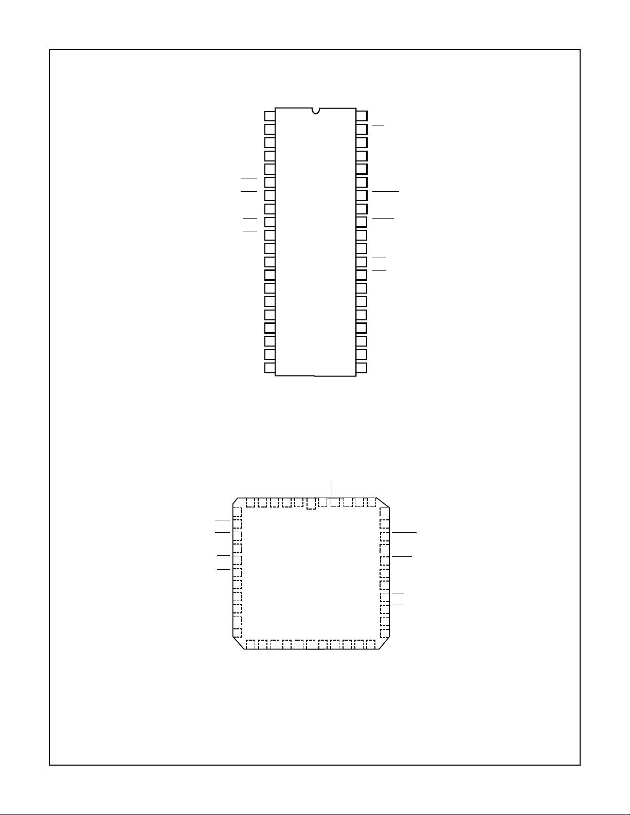
Pinouts
V
DD
429DI1(A)
429DI1(B)
429DI2(A)
429DI2(B)
D/R1
D/R2
SEL
EN1
EN2
BD15
BD14
BD13
BD12
BD11
BD10
BD09
BD08
BD07
BD06
HS-3282
HS-3282 (CERDIP)
TOP VIEW
1
2
3
4
5
6
7
8
9
10
11
12
13
14
15
16
17
18
19
20
40
39
38
37
36
35
34
33
32
31
30
29
28
27
26
25
24
23
22
21
NC
MR
TX CLK
CLK
NC
NC
CWSTR
ENTX
429D0
429D0
TX/R
PL2
PL1
BD00
BD01
BD02
BD03
BD04
BD05
GND
NC
D/R1
D/R2
SEL
EN1
EN2
BD15
BD14
BD13
BD12
BD11
6 3
7
8
9
10
11
12
13
14
15
16
17
NC
NC
429DI2(B)
4
BD10
HS-3282 (CLCC)
TOP VIEW
DD
429DI1(B)
429DI1(A)
429DI2(A)
BD09
BD08
25
BD07
V
1
BD06
NC
44
GND
MR
BD05
TXCLK
CLK
BD04
BD03
40414243
2827262524232221201918
NC
39
38
37
36
35
34
33
32
31
30
29
BD02
NC
NC
CWSTR
ENTX
429D0
429D0
TX/R
PL2
PL1
BD00
BD01
5-184

HS-3282
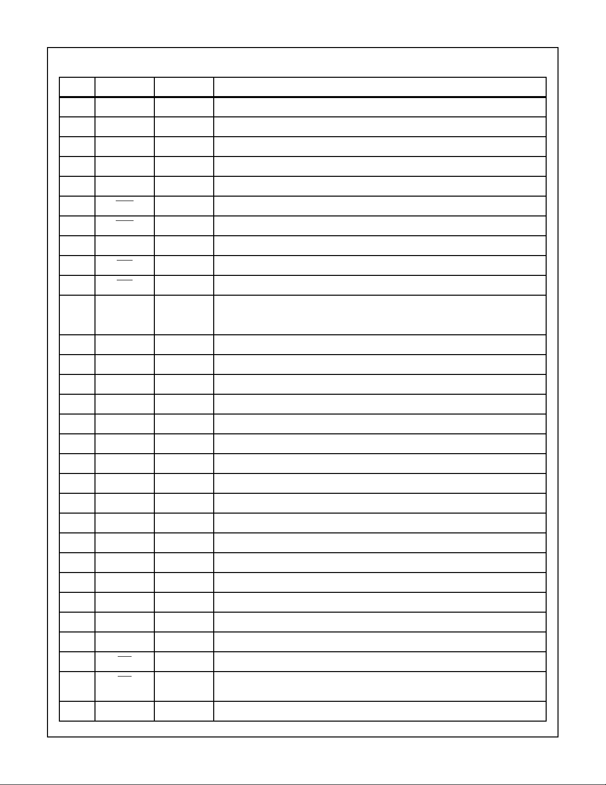
Pin Description
PIN SYMBOL SECTION DESCRIPTION
1VCCRecs/Trans Supply pin 5 volts ±5%.
2 429 DI1 (A) Receiver ARlNC 429 data input to Receiver 1.
3 429 DI1 (B) Receiver ARlNC 429 data input to Receiver 1.
4 429 Dl2 (A) Receiver ARINC 429 data input to Receiver 2.
5 429 DI2 (B) Receiver ARINC 429 data input to Receiver 2.
6 D/R1 Receiver Device ready flag output from Receiver 1 indicating a valid data word is ready to be fetched.
7 D/R2 Receiver Device ready flag output from Receiver 2 indicating a valid data word is ready to be fetched.
8 SEL Receiver Bus Data Selector - Input signal to select one of two 16-bit words from either Receiver 1 or 2.
9 EN1 Receiver Input signal to enable data from Receiver 1 onto the data bus.
10 EN2 Receiver Input signal to enable data from Receiver 2 onto the data bus.
11 BD15 Recs/Trans Bi-directional data bus for fetching data from either of the Receivers, or for loading data into
the Transmitter memory or control word register. See Control Word Table for description of
Control Word bits.
12 BD14 Recs/Trans See Pin 11.
13 BD13 Recs/Trans See Pin 11.
14 BD12 Recs/Trans See Pin 11.
15 BD11 Recs/Trans See Pin 11.
16 BD10 Recs/Trans See Pin 11.
17 BD09 Recs/Trans See Pin 11.
18 BD08 Recs/Trans See Pin 11.
19 BD07 Recs/Trans See Pin 11.
20 BD06 Recs/Trans See Pin 11.
21 GND Recs/Trans Circuit Ground.
22 BD05 Recs/Trans See Pin 11.
23 BD04 Recs/Trans See Pin 11. Control Word function not applicable.
24 BD03 Recs/Trans See Pin 11. Control Word function not applicable.
25 BD02 Recs/Trans See Pin 11. Control Word function not applicable.
26 BD01 Recs/Trans See Pin 11. Control Word function not applicable.
27 BD00 Recs/Trans See Pin 11. Control Word function not applicable.
28 PL1 Transmitter Parallel load input signal loading the first 16-bit word into the Transmitter memory.
29 PL2 Transmitter Parallel load input signal loading the first 16-bit word into the Transmitter memory and initiates
data transfer into the memory stack.
30 TX/R Transmitter Transmitter flag output to indicate the memory is empty.
5-185

HS-3282
Pin Description
PIN SYMBOL SECTION DESCRIPTION
31 429D0 Transmitter Data output from Transmitter
32 429D0 Transmitter Data output from Transmitter.
33 ENTX Transmitter Transmitter Enable input signal to initiate data transmission from FIFO memory.
34 CWSTR Recs/Trans Control word input strobe signal to latch the control word from the databus into the control
35 - - No connection. Must be left open.
36 - - No connection. Must be left open or tied low but never tied high.
37 CLK Recs/Trans External clock input. May be either ten (10) or eighty (80) times the data rate. If using both
38 TXCLK Transmitter Transmitter Clock output. Delivers a clock frequency equal to the transmitter data rate.
39 MR Recs/Trans Master Reset. Active low pulse used to reset FIFO, bit counters, gap timer, word count signal,
40 - - No Connection.
(Continued)
word register.
ARINC data rates it must be ten (10) times the highest data rate, (typically 1MHz).
TX/R and various other flags and controls. Master reset does not reset the control word
register. Usually only used on Power-Up or System Reset.
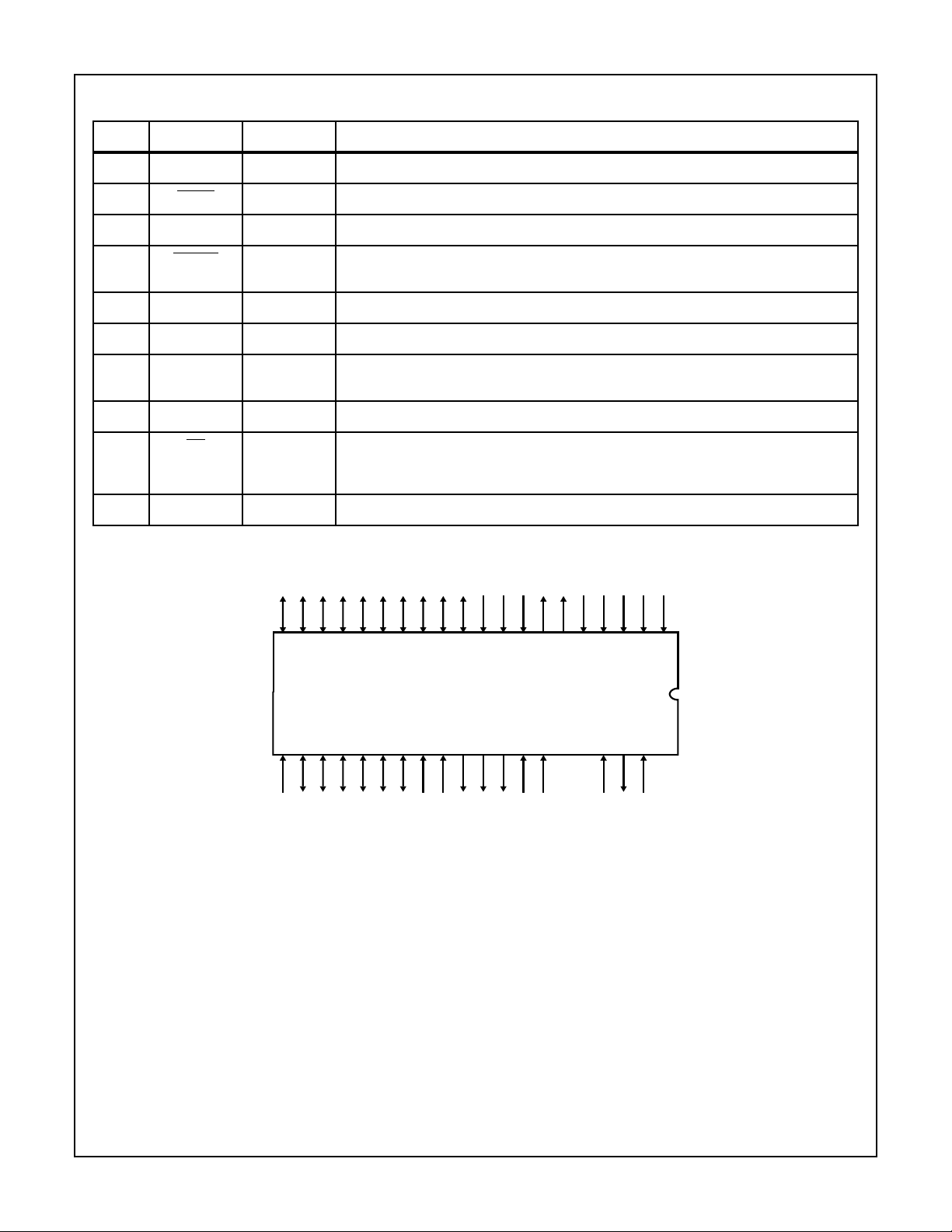
Pinout
13 12345678910111214151617181920
28 40393837363534333231302927262524232221
NCNC NC
5-186

Operational Description
HS-3282
The HS-3282 is designed to support ARINC Specification
429 and other serial data protocols that use a similar format
by collecting the receiving, transmitting, synchronizing,
timing and parity functions on a single, low power LSl circuit.
It goes beyond the ARlNC requirements by providing for
either odd or even parity, and giving the user a choice of
either 25 or 32-bit word lengths. The receiver and transmitter
sections operate independently of each other. The serial-toparallel conversion required of the receiver and the parallelto-serial conversion requirements of the transmitter have
been incorporated into the bus interface circuit.
Provisions have been made through the exter nal clock input
to provide data rate flexibility. This requires an external clock
that is 10 times the data rate.
To obtain the flexibility discussed above, a number of
external control signals are required, To reduce the pin count
requirements, an internal control word register is used. The
control word is latched from the data bus into the register by
the
Control Word Strobe (CWSTR) signal going to a logic
“1”. Eleven (11) control functions are used, and along with
the Bus Data (BD) line are listed below:
Control Word
PIN NAME SYMBOL FUNCTION
BD05 SLFTST Connects the self test signal from the transmitter directly to the receiver shift registers, bypassing the input
receivers. Receiver 1 receives Data True and Receiver 2 receives Data Not. Note that the transmitter output
remains active. (Logic “0” on SLFTST Enables Self Test).
BD06 SDENB1 Signal to Activate the Source/Destination (S/D) Decoder for Receiver 1. (Logic “1” activates S/D Decoder).
BD07 X1 If SDENB1 = “1” then this bit is compared with ARlNC Data Bit #9. If Y1 also matches (see Y1), the word will be
accepted by the Receiver 1. If SDENB1 = “0” this bit becomes a don’t care.
BD08 Y1 If SDENBI = “1” then this bit is compared with ARINC Data Bit #10. If X1 also matches (see X1), the word will
be accepted by the Receiver 1. If SDENB1 = “0” this bit becomes a don’t care.
BD09 SDENB2 Signal to activate the Source/Destination (S/D) Decoder for Receiver 2. (Logic “1” activates S/D Decoder).
BD10 X2 If SDENB2 = “1” then this bit is compared with ARlNC Data Bit #9. If Y2 also matches (see Y2), the word will be
accepted by the Receiver 2. If SDENB2 = “0” this bit becomes a don’t care.
BD11 Y2 If SDENB2 = “1” then this bit is compared with ARINC Data Bit #10. If X2 also matches (see X2), the word will
be accepted by the Receiver 2. If SDENB2 = “0” this bit becomes a don’t care.
BD12 PARCK Signal used to inv ert the transmitter parity bit for test of parity circuits. Logic “0” selects normal odd parity . Logic
“I” selects even parity.
BD13 TXSEL Selects high or low Transmitter data rate. If TXSEL = “0” then transmitter data rate is equal to the clock rate
divided by ten (10). If TXSEL = “1” then transmitter data rate is equal to the clock rate divided by eighty (80).
BD14 RCVSEL Selects high or low Receiver data rate. If RCVSEL = “0” then the receiv ed data rate should be equal to the cloc k
rate divided by ten (10), if RCVSEL = “1 “then the received data rate should be equal to the clock rate divided
by eighty (80).
BD15 WLSEL Selects word length. If WLSEL = “0” a 32-bit word format will be selected. If WLSEL = “1” a 25-Bit word format
will be selected.
ARlNC 429 DATA FORMA T as input to the Receiver and output from the Transmitter is as follows:
TABLE 1. ARINC 429 32-BIT DATA FORMAT
ARINC BIT # FUNCTION
1 - 8 Label
9 - 10 SDl or Data
11 LSB
12 - 27 Data
28 MSB
29 Sign
30, 31 SSM
32 Parity Status
This format is shuffled when seen on the sixteen bidirectional input/outputs. The format shown below is used from
the receivers and input to the transmitter:
TABLE 2A. WORD 1 FORMAT
BI-DIRECTIONAL
BIT # FUNCTION ARINC BlT #
15, 14 Data 13, 12
13 LSB 11
12, 11 SDl or Data 10, 9
10, 9 SSM Status 31, 30
8 Parity Status 32
7 - 00 Label 1 - 8
5-187
 Loading...