

®
www.BDTIC.com/Intersil
HS-3182
Data Sheet May 30, 2008
ARINC 429 Bus Interface Line Driver
Circuit
The HS-3182 is a monolithic dielectric ally isolated bipolar
differential line driver designed to meet the specifications of
ARINC 429. This device is intended to be used with a
companion chip, HS-3282 CMOS ARINC Bus Interface
Circuit, which provides the data formatting and processor
interface function.
All logic inputs are TTL and CMOS compatible. In addition to
the DATA (A) and DATA (B) inputs, there are also inputs for
CLOCK and SYNC signals which are AND’d with the DATA
inputs. This feature enhances system performance and
allows the HS-3182 to be used with devices other than the
HS-3182.
Three power supplies are necessary to operate the HS-3182:
+V = +15V ±10%, -V = -15V ±10%, and V1 = 5V ±5%. V
used to program the differential output voltage swing such that
V
(DIFF) = ±2VREF. Typically, V
OUT
= V1 = 5V ±5%, but a
REF
separate power supply may be used for VREF which should
not exceed 6V .
The driver output impedance is 75Ω ±20% at +25°C. Driver
output rise and fall times are independently programmed
through the use of two external capacitors connected to the CA
and CB inputs. Typical capacitor values are CA = CB = 75pF for
high-speed operation (100kBPS), and CA = CB = 300pF for
low-speed operation (12kBPS to 14.5kBPS). The outputs are
protected against overvoltage and short circuit as shown in the
Block Diagram. The HS-3182 is designed to operate over an
ambient temperature range of -55°C to +125°C, or -40°C to
+85°C.
REF
is
FN2963.3
Features
• RoHS/Pb-free Available for SBDIP Package (100% Gold
Termination Finish)
• TTL and CMOS Compatible Inputs
• Adjustable Rise and Fall Times via Two External
Capacitors
• Programmable Output Differential Voltage via V
REF
Input
• Operates at Data Rates Up to 100k Bits/s
• Output Short Circuit Proof and Contains Overvoltage
Protection
• Outputs are Inhibited (0V) If DATA (A) and DATA (B)
Inputs are Both in the “Logic One” State
• DATA (A) and DATA (B) Signals are “AND’d” with Clock
and Sync Signals
• Full Military Temperature Range
Pinouts
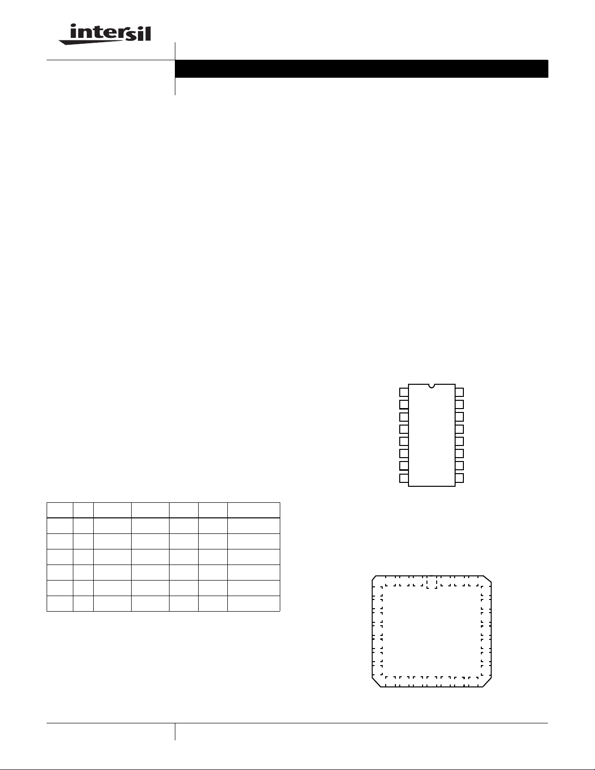
HS-3182
(16 LD SBDIP)
TOP VIEW
V
V
REF
GND
SYNC
DATA (A)
C
A
OUT
GND
1
2
3
4
5
A
6
-V
7
8
16
NC
15
14
CLK
DATA (B)
13
C
12
11
B
10
NC
9
+V
1
B
OUT
TABLE 1. TRUTH TABLE
SYNC C LK DATA (A) DATA (B) A
XL X X 0V0V Null
LX X X 0V 0V Null
HH L L 0V 0V Null
HH L H -V
HH H L+V
HH H H 0V 0V Null
OUTBOUT
REF+VREF
REF-VREF
1
COMMENTS
Low
High
CAUTION: These devices are sensitive to electrostatic discharge; follow proper IC Handling Procedures.
1-888-INTERSIL or 1-888-468-3774
NC
DATA (A)
NC
NC
CA
NC
NC
| Intersil (and design) is a registered trademark of Intersil Americas Inc.
Copyright Intersil Americas Inc. 1997, 2007, 2008. All Rights Reserved
All other trademarks mentioned are the property of their respective owners.
HS-3182
(28 LD CLCC)
TOP VIEW
VREF
NC
28 27 26
+V
GND
V1
NC
BOUT
NC
NC
25
24
23
22
21
20
19
CLK
NC
DATA (B)
CB
NC
NC
NC
SYNC
GND
3 2 14
5
6
7
8
9
10
11
14 15 16 17 1812 13
-V
NC
AOUT
Ordering Information
www.BDTIC.com/Intersil
HS-3182
PART
NUMBER
ORDERING
NUMBER
PART
MARKING
TEMP.
RANGE (°C) PACKAGE
PKG.
DWG. #
HS1-3182-8 5962-8687901EA HS1-3182-8 RD -55 to +125 16 Ld SBDIP, Solder Seal (Pb-free) D16.3
HS1-3182-9+ HS1-3182-9+ HS1-3182-9+ RD -40 to +85 16 Ld SBDIP, Solder Seal (Pb-free) D16.3
HS4-3182-8 5962-86879013A HS4- 3182-8 RD -55 to +125 28 Ld TER CLCC, Solder Seal J28.A
NOTE: These Intersil Pb-free Hermetic packaged products employ 100% Au plate - e4 termination finish, which is RoHS compliant and compatible
with both SnPb and Pb-free soldering operations.
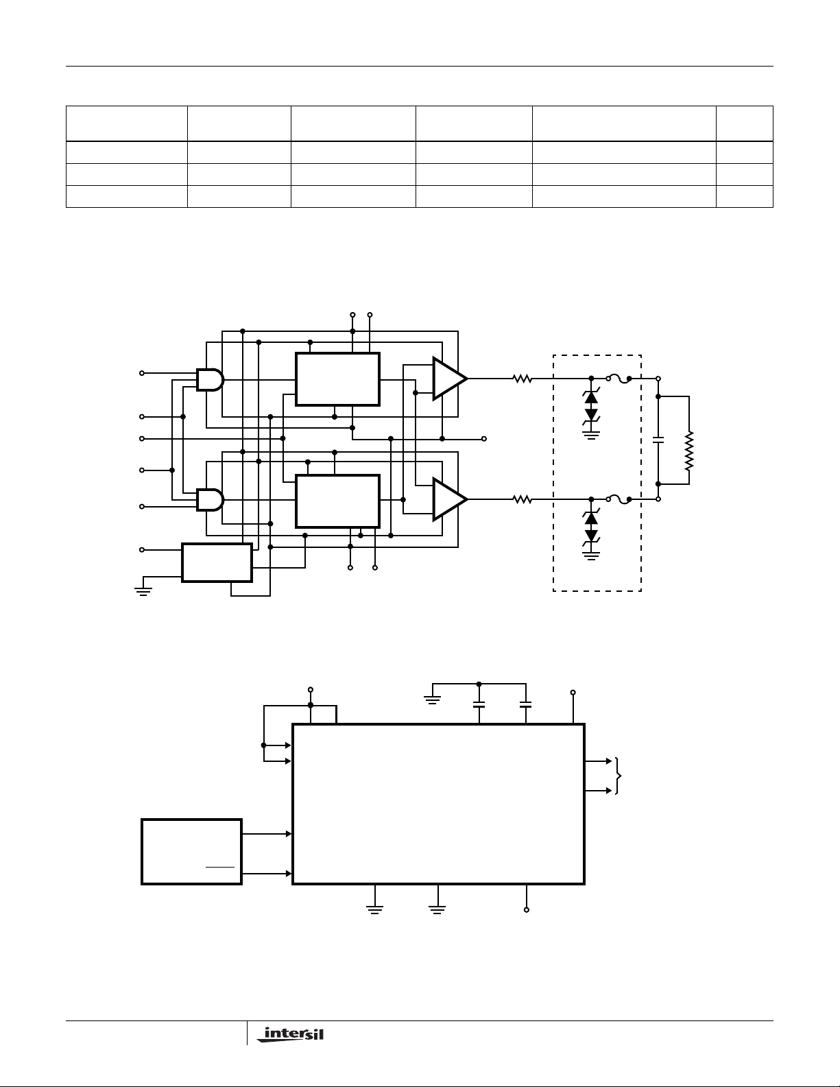
Block Diagram
(9) (5)
+V CA
OUTPUT
DATA (A)
CLOCK
VREF
SYNC
DATA (B)
(4)
(14)
(1)
(3)
(13)
LEVEL SHIFTER
AND SLOPE
CONTROL (A)
LEVEL SHIFTER
AND SLOPE
CONTROL (B)
DRIVER
(A)
(8)
OUTPUT
DRIVER
(B)
ROUT/2
GND
ROUT/2
F
FB
(6)
A
AOUT
CL
RL
BOUT
(11)
(16)
V1
(2)
CURRENT
REGULATOR
Typical Application
PIN NUMBERS INDICATED BY ( )
HS-3282
CMOS ARINC
CIRCUIT
429D0
429D0
C
B
(7)(8)(2)
OVER-VOLTAGE
PROTECTION
(9)
+15V
+V
AOUT
BOUT
PIN NUMBER 10, 15 = NC
TO BUS
(SEE NOTE)
-V CB
(7) (12)
+5V
(1)(16)
V1 VREF C
(14)
CLOCK
(3)
SYNC
HS-3182
ARINC DRIVER
31
(4)
DATA (A)
32
(13)
DATA (B)
CIRCUIT
16 LEAD DIP
GNDGND -V
CA CB
(12)(5)
A
-15V
NOTE: The rise and fall time of the outputs are set to ARINC specified values by CA and CB. Typical CA = CB = 75pF for high speed and 300pF for
low speed operation. The output HI and low levels are set to ARINC specifications by V
REF
.
2
FN2963.3
May 30, 2008
HS-3182
www.BDTIC.com/Intersil
Absolute Maximum Ratings Thermal Information
Voltage Between +V and -V Terminals . . . . . . . . . . . . . . . . . . . .40V
V1. . . . . . . . . . . . . . . . . . . . . . . . . . . . . . . . . . . . . . . . . . . . . . . . . .7V
VREF . . . . . . . . . . . . . . . . . . . . . . . . . . . . . . . . . . . . . . . . . . . . . . .6V
Logic Input Voltage . . . . . . . . . . . . . . . . . . . GND -0.3V to V1 +0.3V
Output Short Circuit Duration. . . . . . . . . . . . . . . . . . . . . . . . (Note 3)
Output Overvoltage Protection. . . . . . . . . . . . . . . . . . . . . . . (Note 4)
Thermal Resistance (Typical) θ
SBDIP Package . . . . . . . . . . . . . . . . . . 68 12
CLCC Package . . . . . . . . . . . . . . . . . . 54 10
Storage Temperature Range . . . . . . . . . . . . . . . . . .-65°C to +150°C
Maximum Junction Temperature . . . . . . . . . . . . . . . . . . . . . . +175°C
Pb-free reflow profile . . . . . . . . . . . . . . . . . . . . . . . . . .see link below
http://www.intersil.com/pbfree/Pb-FreeReflow.asp
Operating Conditions
Operating Voltage
+V . . . . . . . . . . . . . . . . . . . . . . . . . . . . . . . . . . . . . . . +15V ±10%
-V . . . . . . . . . . . . . . . . . . . . . . . . . . . . . . . . . . . . . . . . . -15V ±10%
V1. . . . . . . . . . . . . . . . . . . . . . . . . . . . . . . . . . . . . . . . . . . 5V ±5%
VREF (For ARINC 429) . . . . . . . . . . . . . . . . . . . . . . . . . . 5V ±5%
Operating Temperature Range
HS-3182-9+ . . . . . . . . . . . . . . . . . . . . . . . . . . . . . .-40°C to +85°C
HS-3182-8 . . . . . . . . . . . . . . . . . . . . . . . . . . . . . .-55°C to +125°C
CAUTION: Do not operate at or near the maximum ratings listed for extended periods of time. Exposure to such conditions may adversely impact product reliability and
result in failures not covered by warranty.
NOTES:
1. θ
is measured with the component mounted on a low effective thermal conductivity test board in free air. See Tech Brief TB379 for details.
JA
, the “case temp” location is the center of the package underside.
2. θ
JC
3. Heat sink may be required for 100k bits/s at +125°C and output short circuit at +125°C.
4. The fuses used for output overvoltage protection may be blown by a fault at each output of greater than ±6.5V relative to GND.
Die Characteristics
Number of Transistors or Gates . . . . . . . . . . . . . . . . . . . . . . . . . 133
(°C/W) θJC (°C/W)
JA
DC Electrical Specifications Parameters with MIN and/or MAX limits are 100% tested at +25°C, unless otherwise specified.
Temperature limits established by characterization and are not production tested.
CONDITIONS
DC PARAMETER SYMBOL
Supply Current +V (Operating) I
Supply Current -V (Operating) I
Supply Current V
Supply Current V
Logic “1” Input Voltage V
Logic “0” Input Voltage V
Output Voltage High (Output to GND) V
Output Voltage Low (Output to GND) V
Output Voltage Null V
Input Current (Input Low) I
Input Current (Input High) I
Output Short Circuit Current
(Output High)
Output Short Circuit Current
(Output Low)
Output Impedance Z
NOTES:
5. +V = +15V ±10%, -V = -15V ±10%, V
= -55°C to +125°C for HS-3182-8.
T
A
(Operating) I
1
(Operating) I
REF
1
= V
CCOP
CCOP
CCOP
CCOP
REF
(+V) No Load (0k to 100k bits/s) - 16 mA
(-V) No Load (0k to 100k bits/s) -16 - mA
(V1) No Load (0k to 100k bits/s) - 975 µA
(V
) No Load (0k to 100k bits/s) -1.0 - mA
REF
IH
IL
OH
OL
NULL
IL
IH
I
OHSC
I
OLSC
O
= 5V ±5%, unless otherwise specified TA = -40°C to +85°C for HS-3182-9+ and
No Load (0k to 100k bits/s) V
No Load (0k to 100k bits/s) -V
No Load (0k to 100k bits/s) -250 +250 mV
Short to GND - -80 mA
Short to GND 80 - mA
TA = +25°C 60 90 Ω
(Note 5) MIN MAX UNITS
2.0 - V
-0.5V
REF
(-250mV)
REF
(-250mV)
-20 - mA
-10mA
V
REF
(+250mV)
-V
REF
(+250mV)
3
FN2963.3
May 30, 2008

HS-3182
www.BDTIC.com/Intersil
AC Electrical Specifications
AC PARAMETER SYMBOL
, B
Rise Time (A
Fall Time (A
Propagation Delay Input to Output t
Propagation Delay Input to Output t
NOTES:
6. +V = +15V, -V = -15V, V
HS-3182-8.
7. t
R
8. t
F
OUT
OUT
measured 50% to 90% x 2, no load.
measured 50% to 10% x 2, no load.
)t
OUT
, B
)t
OUT
= V
1
= 5V, unless otherwise specified TA = -40°C to +85°C for HS-3182-9+ and TA = -55°C to +125°C for
REF
PLH
PHL
CA = CB = 75pF, (Note 7) 1 2 µs
R
= -55°C Only) 0.9 2.4 µs
(at T
A
= CB = 300pF, (Note 7) 3 9 µs
C
A
CA = CB = 75pF, (Note 8) 1 2 µs
F
= -55°C Only) 0.9 2.4 µs
(at T
A
CA = CB = 300pF, (Note 8) 3 9 µs
CA = CB = 75pF, No Load - 3.3 µs
CA = CB = 75pF, No Load - 3.3 µs
Electrical Specifications
PARAMETER SYMBOL
Input Capacitance C
Supply Current +V (Short Circuit) I
Supply Current -V (Short Circuit) ISC (-V) Short to GND, TA = +25°C -150 - mA
NOTES:
9. Limits established by characterization and are not production tested.
(+V) Short to GND, TA = +25°C - 150 mA
SC
TA = +25°C - 15 pF
IN
CONDITIONS
(Note 6) MIN MAX UNITS
CONDITIONS
(NOTE 9) MIN MAX UNITS
Power Specifications Nominal Power at +25°C, +V = +15V, -V = -15V, V1 = VREF = 5V, Notes 10, 12
DATA RATE
(k BITS/s) LOAD +V V- V
0 to 100 No Load 11mA -10mA 600µA 325mW 0
12.5 to 14 Full Load, Note 11 24mA -24mA 600µA 660mW 60mW
100 Full Load, Note 11 46mA -46mA 600µA 1 Watt 325mW
NOTES:
10. Heat sink may be required for 100k bits/s at +125°C and output short circuit at +125°C.
Thermal characteristics: T
Where: T
11. Full Load for ARINC 429: R
12. Output Overvoltage Protection: The fuses used for output overvoltage protection may be blown by a fault at each output of greater than ±6.5V
relative to GND.
(Junction Max)
θ
(Junction - Case)
θ
(Junction - Ambient)
= +175°C
= T
(CASE)
= 10.9°C/W (6.1°C/W for LCC)
= 73.5°C/W (54.0°C/W for LCC)
L
(Junction)
= 400Ω and CL = 30,000pF in parallel between A
- θ
(Junction - Case) P(Dissipation)
.
OUT
1
and B
CHIP POWER
(See “Block Diagram” on page 2).
OUT
POWER DISSIPATION IN
LOAD
4
FN2963.3
May 30, 2008

Driver Waveforms
www.BDTIC.com/Intersil
HS-3182
NOTES:
A
V
0V
0V
-V
OUT
0V
REF
t
PHL
REF
- B
50%
50%
OUT
DATA (A) 0V
DATA (B) 0V
A
OUT
B
OUT
DIFFERENTIAL
OUTPUT
measured 50% to 90% x 2
t
R
measured 50% to 10% x 2
t
F
= 5V VOL = -4.75V to -5.25V
V
IH
V
= 0V VOH = 4.75V to 5.25V
IL
ADJ. BY
C
A
t
R
-2V
REF
50%
ADJ. BY
C
B
50%
2V
REF
t
F
t
PLH
5V
0V
5V
0V
+4.75V TO +5.25V
-V
REF
V
REF
HIGH
NULL
LOW
-4.75V TO -5.25V
+4.75V TO +5.25V
-4.75V TO -5.25V
+9.5V TO +10.5V
NOTE: OUTPUTS UNLOADED
-9.5V TO -10.5V
When the Data (A) input is in the Logic One state and the Data (B)
input is in the Logic Zero state, A
equal to -V
Data (B) both in the Logic Zero state causes both A
. This constitutes the Output High state. Data (A) and
REF
is equal to V
OUT
REF
OUT
to be equal to 0V which designates the output Null state. Data (A) in
the Logic Zero state and Data (B) in the Logic One state causes
to be equal to -V
A
OUT
REF
and B
to be equal to V
OUT
the Output Low state.
and B
and B
which is
REF
OUT
is
OUT
Burn-In Schematic
NOTES:
V
16 15 14 13 12 11 10 9
12345678
R = 400Ω ± 5%
= 0.03mF ± 20%
C
1
= C3 = 500pF, NPO
C
2
+V = +15.5V ± 0.5V
-V = -15.5V ± 0.5V
V
= +5.5V ± 0.5V
1
A 0.0mF decoupling capacitor is required on each of the three
supply lines (+V, -V and V
DATA (B) +V
1
HS-3182
C
3
R
C
2
-VDATA (A)
) at every 3rd Burn-In socket.
1
C
1
GND
A
B
Ambient Temp. Max. = +125°C.
Package = 16 Lead Side Brazed DIP.
Pulse Conditions = A & B = 6.25kHz ±10%. B is delayed one-half
cycle and in sync with A.
V
= 2.0V Min.
IH
= 0.5V Max.
V
IL
V
IH
V
IL
V
IH
V
IL
5
FN2963.3
May 30, 2008

HS-3182
www.BDTIC.com/Intersil
Ceramic Leadless Chip Carrier Packages (CLCC)
j x 45
E1
o
B
h x 45
-E-
E2
e1
o
A
-F-
0.010 E HS S
L
D
D3
0.007 E FM S HS
B1
L2
D1
-H-
D2
B2
J28.A MIL-STD-1835 CQCC1-N28 (C-4)
28 PAD CERAMIC LEADLESS CHIP CARRIER PACKAGE
INCHES MILLIMETERS
SYMBOL
A 0.060 0.100 1.52 2.54 6, 7
A1 0.050 0.088 1.27 2.23 -
B-----
B1 0.022 0.028 0.56 0.71 2, 4
E
E3
0.010 E FSS
A1
PLANE 2
PLANE 1
e
L3
B3
L1
B2 0.072 REF 1.83 REF -
B3 0.006 0.022 0.15 0.56 -
D 0.442 0.460 11.23 11.68 -
D1 0.300 BSC 7.62 BSC -
D2 0.150 BSC 3.81 BSC -
D3 - 0.460 - 11.68 2
E 0.442 0.460 11.23 11.68 -
E1 0.300 BSC 7.62 BSC -
E2 0.150 BSC 3.81 BSC -
E3 - 0.460 - 11.68 2
e 0.050 BSC 1.27 BSC -
e1 0.015 - 0.38 - 2
h 0.040 REF 1.02 REF 5
j 0.020 REF 0.51 REF 5
L 0.045 0.055 1.14 1.40 -
L1 0.045 0.055 1.14 1.40 -
L2 0.075 0.095 1.90 2.41 -
L3 0.003 0.015 0.08 0.038 -
ND 7 7 3
NE 7 7 3
N28 283
NOTES:
1. Metallized castellations shall be connected to plane 1 terminals
and extend toward plane 2 across at least two layers of ceramic
or completely across all of the ceramic layers to make electrical
connection with the optional plane 2 terminals.
2. Unless otherwise specified, a minimum clearance of 0.015 inch
(0.38mm) shall be maintained between all metallized features
(e.g., lid, castellations, terminals, thermal pads, etc.)
3. Symbol “N” is the maximum number of terminals. Symbols “ND”
and “NE” are the number of terminals along the sides of length
“D” and “E”, respectively.
4. The required plane 1 terminals and optional plane 2 terminals (if
used) shall be electrically connected.
5. The corner shape (square, notch, radius, etc.) may vary at the
manufacturer’s option, from that shown on the drawing.
6. Chip carriers shall be constructed of a minimum of two ceramic
layers.
7. Dimension “A” controls the overall package thickness. The maximum “A” dimension is package height before being solder dipped.
8. Dimensioning and tolerancing per ANSI Y14.5M-1982.
9. Controlling dimension: INCH.
NOTESMIN MAX MIN MAX
Rev. 0 5/18/94
6
FN2963.3
May 30, 2008

HS-3182
www.BDTIC.com/Intersil
Ceramic Dual-In-Line Metal Seal Packages (SBDIP)
LEAD FINISH
c1
-A-
-B-
S
bbb C A - B
BASE
PLANE
SEATING
PLANE
S1
b2
ccc
b
CA - BM
D
A
A
e
DS S
NOTES:
1. Index area: A notch or a pin one identification mark shall be located adjacent to pin one and shall be located within the shaded
area shown. The manufacturer’s identification shall not be used
as a pin one identification mark.
2. The maximum limits of lead dimensions b and c or M shall be
measured at the centroid of the finished lead surfaces, when
solder dip or tin plate lead finish is applied.
3. Dimensions b1 and c1 apply to lead base metal only. Dimension
M applies to lead plating and finish thickness.
4. Corner leads (1, N, N/2, and N/2+1) may be configured with a
partial lead paddle. For this configuration dimension b3 replaces
dimension b2.
5. Dimension Q shall be measured from the seating plane to the
base plane.
6. Measure dimension S1 at all four corners.
7. Measure dimension S2 from the top of the ceramic body to the
nearest metallization or lead.
8. N is the maximum number of terminal positions.
9. Braze fillets shall be concave.
10. Dimensioning and tolerancing per ANSI Y14.5M - 1982.
11. Controlling dimension: INCH.
-D-
BASE
E
S
S
D
Q
S2
-C-
METAL
b1
M
(b)
SECTION A-A
A
L
(c)
M
eA
aaa
eA/2
CA - BM DS S
c
D16.3 MIL-STD-1835 CDIP2-T16 (D-2, CONFIGURATION C)
16 LEAD CERAMIC DUAL-IN-LINE METAL SEAL PACKAGE
INCHES MILLIMETERS
SYMBOL
A - 0.200 - 5.08 -
b 0.014 0.026 0.36 0.66 2
b1 0.014 0.023 0.36 0.58 3
b2 0.045 0.065 1.14 1.65 -
b3 0.023 0.045 0.58 1.14 4
c 0.008 0.018 0.20 0.46 2
c1 0.008 0.015 0.20 0.38 3
D - 0.840 - 21.34 -
E 0.220 0.310 5.59 7.87 -
e 0.100 BSC 2.54 BSC -
eA 0.300 BSC 7.62 BSC -
eA/2 0.150 BSC 3.81 BSC -
L 0.125 0.200 3.18 5.08 -
Q 0.015 0.060 0.38 1.52 5
S1 0.005 - 0.13 - 6
S2 0.005 - 0.13 - 7
o
α
90
105
o
90
o
105
aaa - 0.015 - 0.38 -
bbb - 0.030 - 0.76 -
ccc - 0.010 - 0.25 -
M - 0.0015 - 0.038 2
N16 168
NOTESMIN MAX MIN MAX
o
Rev. 0 4/94
-
All Intersil U.S. products are manufactured, assembled and tested utilizing ISO9000 quality systems.
Intersil Corporation’s quality certifications can be viewed at www.intersil.com/design/quality
Intersil products are sold by description only. Intersil Corporation reserves the right to make changes in circuit design, software and/or specifications at any time without
notice. Accordingly, the reader is cautioned to verify that data sheets are current before placing orders. Information furnished by Intersil is believed to be accurate and
reliable. However, no responsibility is assumed by Intersil or its subsidiaries for its use; nor for any infringements of patents or other rights of third parties which may result
from its use. No license is granted by implic atio n or other wise u nde r any p a tent or patent rights of Intersil or its subsidiaries.
For information regarding Intersil Corporation and its products, see www.intersil.com
7
FN2963.3
May 30, 2008
 Loading...