Intersil Corporation HS-307RH-883S, HS-384RH-883S, HS-390RH-883S, HS-302RH-883S, HS-303RH-883S Datasheet
...
September 1995
HS-302RH/883S, HS-303RH/883S,
HS-306RH/883S, HS-307RH/883S,
HS-384RH/883S, HS-390RH/883S
Radiation Hardened
CMOS Analog Switches
Features
• This Circuit is Processed in Accordance to Mil-Std883 and is Fully Conformant Under the Provisions of
Paragraph 1.2.1.
• Radiation Hardened
- Functional Total Dose Exceeds 1 x 10
• Pin for Pin Compatible with Intersil HI-3XX Series
Analog Switches
• Analog Signal Range 15V
• Low Leakage
•Low R
• No Latch Up
• Versions for 5V and 15V Digital Systems
• Low Operating Power
• Military Temperature Range -55
ON
o
C to +125oC
5
RAD Si
Applications
• Sample and Hold i.e. Low Leakage Switching
• Op Amp Gain Switching i.e. Low ON Resistance
• Switched Capacitor Filters
• Low Level Switching Circuits
• Satellites
• Nuclear Reactor Controls
• Military Environments
Description
The HS-3XXRH/883S family of analog switches are
monolithic devices fabricated using Radiation Hardened
CMOS technology and the Intersil dielectric isolation process for latch-up free operation. Improved total dose hardness is obtained by layout (thin oxide tabs extending to a
channel stop) and processing (hardened gate oxide). These
switches offer low-resistance switching performance for analog voltages up to the supply rails. “ON” resistance is low
and stays reasonably constant over the full range of operating voltage and current. “ON” resistance also stays reasonably constant when exposed to radiation, being typically 30Ω
pre-rad and 35Ω post 100K RAD-Si. All devices provide
break-before-make switching.
The 6 devices in this switch series are differentiated by type
of switch action, pinout and digital logic levels. The HS-302/
303/384/390RH/883S switches have 5V digital inputs while
the HS-306/307RH/883S switches have 15V digital inputs.
All devices are available in Ceramic Flatpack and SBDIP
packages. The HS-3XXRH/883S switches can directly
replace the HI-3XX series devices.
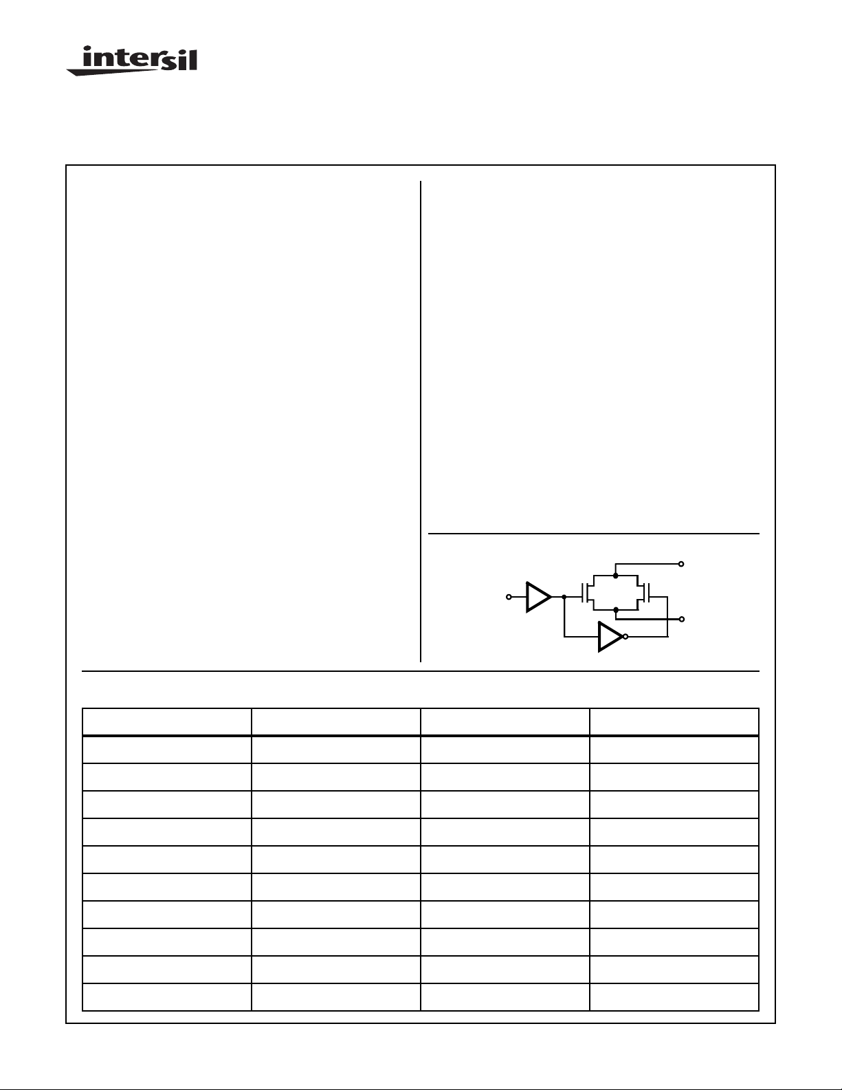
Functional Diagram
IN
N P
D
Ordering Information
PART NUMBER TEMPERATURE RANGE SCREENING LEVEL PACKAGE
HS1-302RH/883S -55oC to +125oC Intersil /883 Class S Equivalent 14 Lead SBDIP
HS9-302RH/883S -55oC to +125oC Intersil /883 Class S Equivalent 14 Lead Ceramic Flatpack
HS1-302RH/Sample +25oC Sample 14 Lead SBDIP
HS9-302RH/Sample +25oC Sample 14 Lead Ceramic Flatpack
HS1-303RH/883S -55oC to +125oC Intersil /883 Class S Equivalent 14 Lead SBDIP
HS9-303RH/883S -55oC to +125oC Intersil /883 Class S Equivalent 14 Lead Ceramic Flatpack
HS1-303RH/Sample +25oC Sample 14 Lead SBDIP
HS9-303RH/Sample +25oC Sample 14 Lead Ceramic Flatpack
HS1-306RH/883S ( Note 1) -55oC to +125oC Intersil /883 Class S Equivalent 14 Lead SBDIP
HS9-306RH/883S ( Note 1) -55oC to +125oC Intersil /883 Class S Equivalent 14 Lead Ceramic Flatpack
CAUTION: These devices are sensitive to electrostatic discharge; follow proper IC Handling Procedures.
http://www.intersil.com or 407-727-9207 | Copyright © Intersil Corporation 1999
1
Spec Number 518526
File Number 3067.1
HS-3XXRH/883S
Ordering Information
(Continued)
PART NUMBER TEMPERATURE RANGE SCREENING LEVEL PACKAGE
HS1-306RH/Sample (Note 1) +25oC Sample 14 Lead SBDIP
HS9-306RH/Sample (Note 1) +25oC Sample 14 Lead Ceramic Flatpack
HS1-307RH/883S -55oC to +125oC Intersil /883 Class S Equivalent 14 Lead SBDIP
HS9-307RH/883S -55oC to +125oC Intersil /883 Class S Equivalent 14 Lead Ceramic Flatpack
HS1-307RH/Sample +25oC Sample 14 Lead SBDIP
HS9-307RH/Sample +25oC Sample 14 Lead Ceramic Flatpack
HS1-384RH/883S (Note 1) -55oC to +125oC Intersil /883 Class S Equivalent 16 Lead SBDIP
HS9-384RH/883S (Note 1) -55oC to +125oC Intersil /883 Class S Equivalent 16 Lead Ceramic Flatpack
HS1-384RH/Sample (Note 1) +25oC Sample 16 Lead SBDIP
HS9-384RH/Sample (Note 1) +25oC Sample 16 Lead Ceramic Flatpack
HS1-390RH/883S -55oC to +125oC Intersil /883 Class S Equivalent 16 Lead SBDIP
HS9-390RH/883S -55oC to +125oC Intersil /883 Class S Equivalent 16 Lead Ceramic Flatpack
HS1-390RH/Sample +25oC Sample 16 Lead SBDIP
HS9-390RH/Sample +25oC Sample 16 Lead Ceramic Flatpack
NOTE:
1. Not recommended for new design.
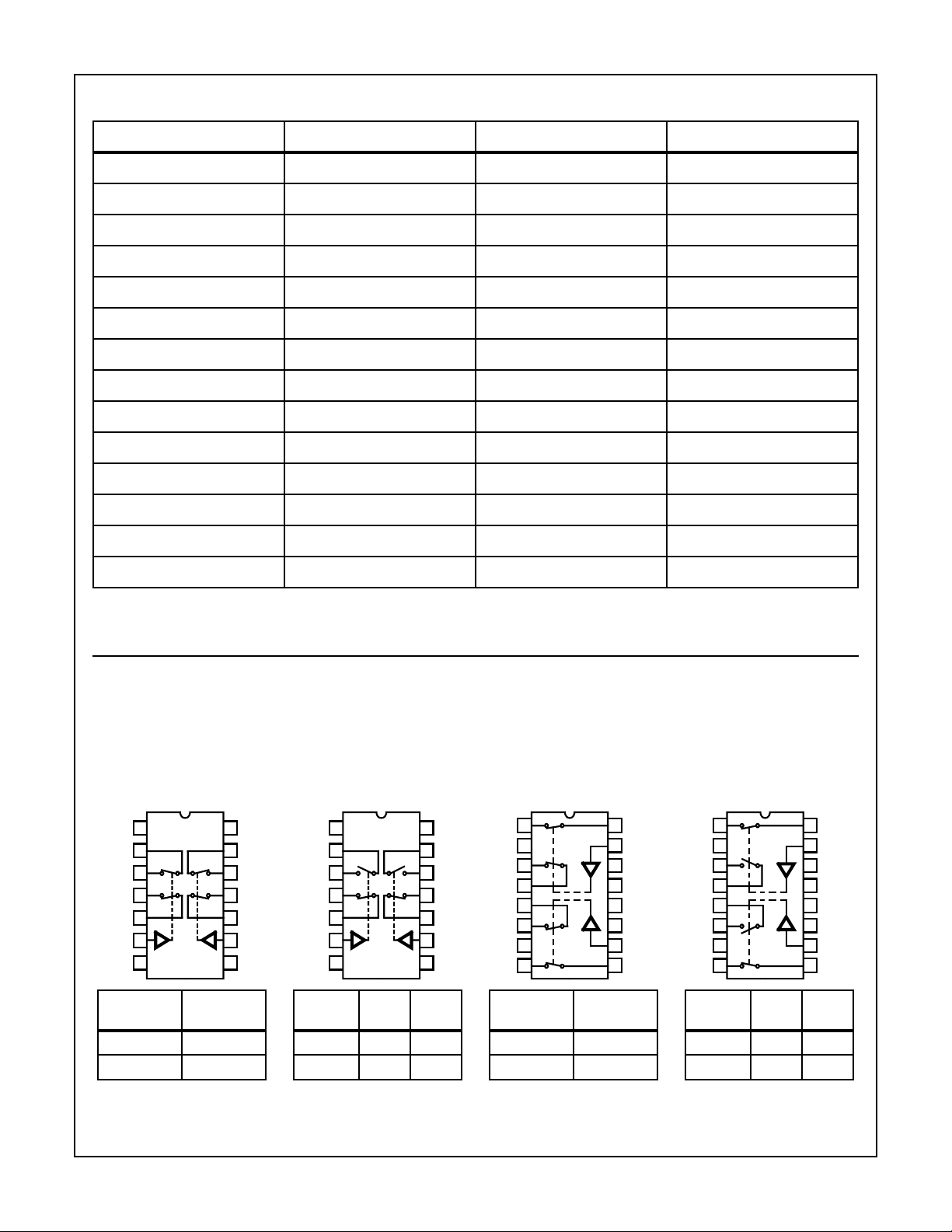
Pinouts
NC
S3
D3
D1
S1
IN1
GND
LOGIC
(Switch States are for Logic “1” Inputs)
14 LEAD CERAMIC DUAL-IN-LINE
METAL SEAL PACKAGE (SBDIP)
MIL-STD-1835 CDIP2-T14
TOP VIEW
DUAL DPST
HS-302RH/883S
HS-306RH/883S
1
2
3
4
5
6
7
14
V+
13
S4
12
D4
11
D2
10
S2
9
IN2
8
V-
GND
SWITCH
1 - 4
0 OFF
1ON
DUAL SPDT
HS-303RH/883S
HS-307RH/883S
1
NC
2
S3
3
D3
4
D1
5
S1
6
IN1
7
SW1
LOGIC
SW2
0 OFF ON
1 ON OFF
14
13
12
11
10
9
8
SW3
SW4
V+
S4
D4
D2
S2
IN2
V-
16 LEAD CERAMIC DUAL-IN-LINE
METAL SEAL PACKAGE (SBDIP)
MIL-STD-1835 CDIP2-T16
DUAL DPST
HS-384RH/883S
D1
NC
D3
S3
S4
D4
NC
D2
1
2
3
4
5
6
7
8
16
15
14
13
12
11
10
9
SWITCH
LOGIC
1 - 4
0 OFF
1ON
TOP VIEW
S1
IN1
VGND
NC
V+
IN2
S2
DUAL SPDT
HS-390RH/883S
1
D1
2
NC
3
D3
4
S3
5
S4
6
D4
7
NC
8
D2
SW1
LOGIC
SW2
0 OFF ON
1 ON OFF
16
15
14
13
12
11
10
9
S1
IN1
VGND
NC
V+
IN2
S2
SW3
SW4
Spec Number 518526
2
HS-3XXRH/883S
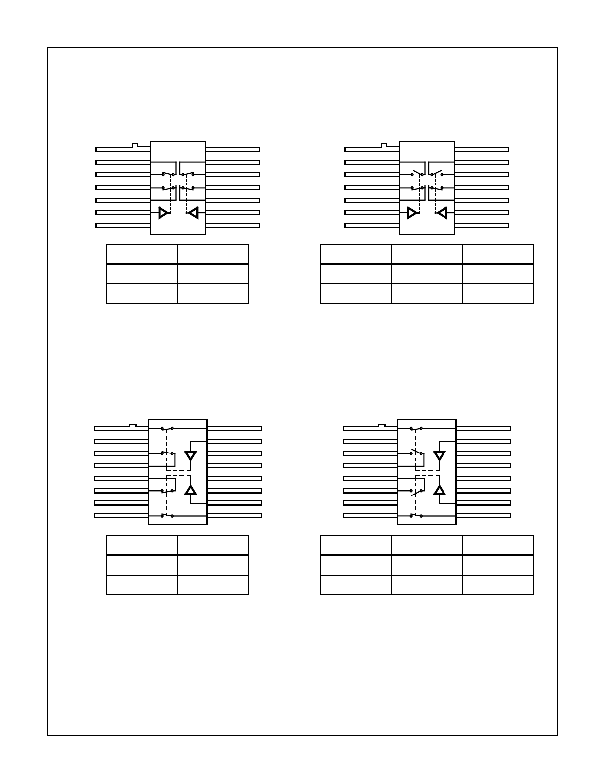
Pinouts
NC
S3
D3
D1
S1
IN1
GND
(Switch States are for Logic “1” Inputs) (Continued)
14 LEAD CERAMIC METAL SEAL FLATPACK PACKAGE (FLATPACK)
MIL-STD-1835 CDIP3-F14
DUAL DPST
HS-302RH/883S
HS-306RH/883S
1
2
3
4
5
6
7
14
13
12
11
10
9
8
V+
S4
D4
D2
S2
IN2
V-
LOGIC SWITCH 1 - 4
0 OFF
1ON
TOP VIEW
DUAL SPDT
HS-303RH/883S
HS-307RH/883S
NC
S3
D3
D1
S1
IN1
GND
1
2
3
4
5
6
7
14
13
12
11
10
9
8
LOGIC SW1 AND SW2 SW3 AND SW4
0 OFF ON
1 ON OFF
V+
S4
D4
D2
S2
IN2
V-
D1
NC
D3
S3
S4
D4
NC
D2
16 LEAD CERAMIC METAL SEAL FLATPACK PACKAGE (FLATPACK)
DUAL DPST
HS-384RH/883S
116
2
3
4
5
6
7
8
15
14
13
12
11
10
9
LOGIC SWITCH 1 - 4
0 OFF
1ON
MIL-STD-1835 CDIP4-F16
TOP VIEW
S1
IN1
VGND
NC
V+
IN2
S2
D1
NC
D3
S3
S4
D4
NC
D2
DUAL SPDT
HS-390RH/883S
116
2
3
4
5
6
7
8
15
14
13
12
11
10
9
S1
IN1
VGND
NC
V+
IN2
S2
LOGIC SW1 AND SW2 SW3 AND SW4
0 OFF ON
1 ON OFF
Spec Number 518526
3
Specifications HS-3XXRH/883S
Absolute Maximum Ratings Reliability Information
Supply Voltage Between V+ and V- . . . . . . . . . . . . . . . . . . . . . +44V
+VSUPPLY to Ground . . . . . . . . . . . . . . . . . . . . . . . . . . . . . . . +22V
-VSUPPLY to Ground. . . . . . . . . . . . . . . . . . . . . . . . . . . . . . . . .-22V
Analog Input Overvoltages:
+VS. . . . . . . . . . . . . . . . . . . . . . . . . . . . . . . . . . +VSUPPLY +1.5V
-VS . . . . . . . . . . . . . . . . . . . . . . . . . . . . . . . . . . .-VSUPPLY - 1.5V
Digital Input Overvoltage:
+VA. . . . . . . . . . . . . . . . . . . . . . . . . . . . . . . . . . . .+VSUPPLY +4V
-VA . . . . . . . . . . . . . . . . . . . . . . . . . . . . . . . . . . . . .-VSUPPLY -4V
Peak Current, S or D Pulsed at 1ms, 10% Duty Cycle Max. . .40mA
Continuous Current . . . . . . . . . . . . . . . . . . . . . . . . . . . . . . . . .10mA
Storage Temperature Range . . . . . . . . . . . . . . . . . -65oC to +150oC
Junction Temperature. . . . . . . . . . . . . . . . . . . . . . . . . . . . . . +175oC
Lead Temperature (soldering 10s) . . . . . . . . . . . . . . . . . . . . .≤ +300oC
CAUTION: Stresses above those listed in “Absolute Maximum Ratings” may cause permanent damage to the device. This is a stress only rating and operation
of the device at these or any other conditions above those indicated in the operational sections of this specification is not implied.
Operating Conditions
Operating Supply Voltage (± VSupply) . . . . . . . . . . . . . . . . . . . . . ±15V Operating Temperature Range . . . . . . . . . . . . . . . .-55oC to +125oC
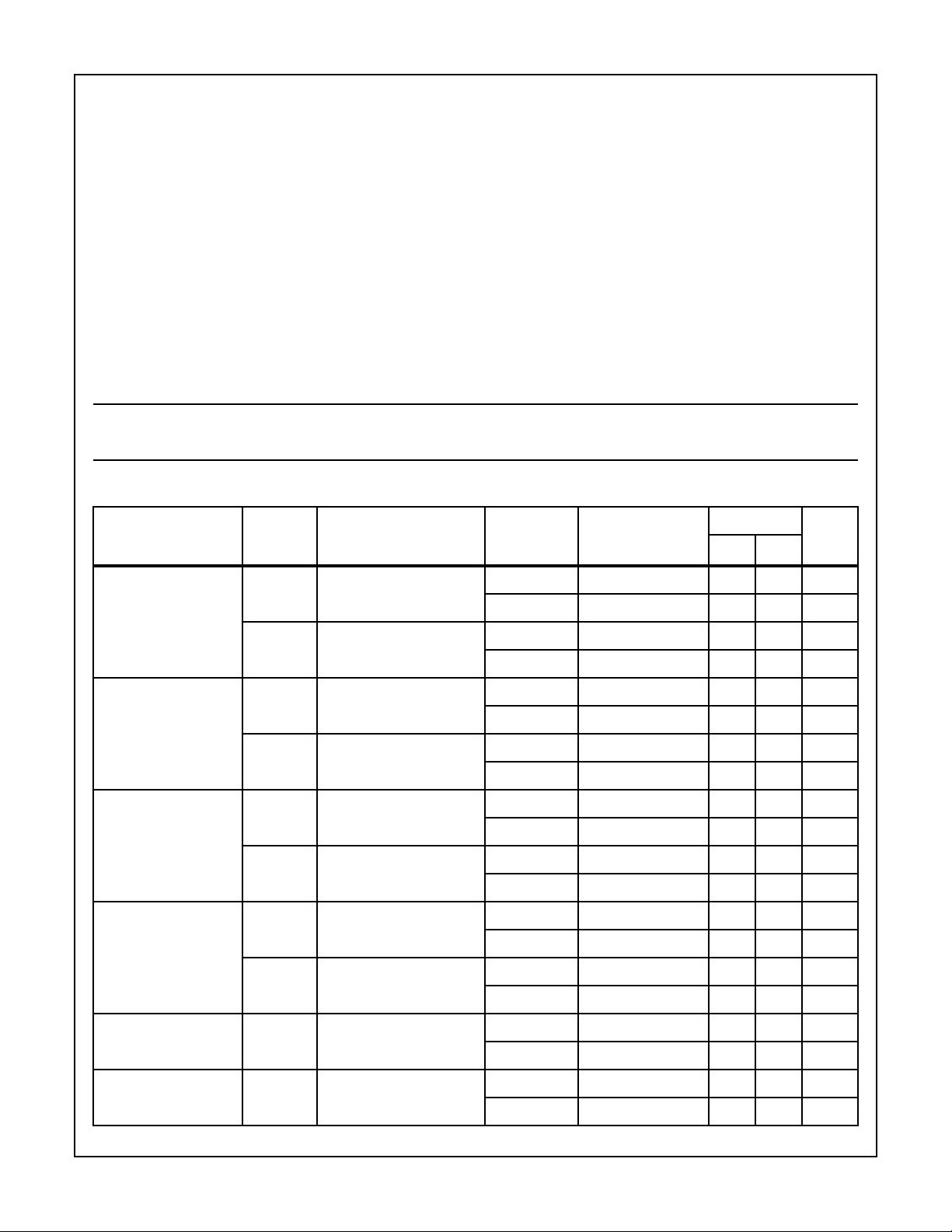
TABLE 1. HS-302RH/303RH/384RH/390RH/883S DC ELECTRICAL PERFORMANCE CHARACTERISTICS
Device Guaranteed and 100% Tested. Unless Otherwise Specified: V- = -15V, V+ = +15V, VAH = +4.0V, VAL = 0.8V
PARAMETER SYMBOL CONDITIONS
Thermal Resistance θ
14 Lead SBDIP Package. . . . . . . . . . . . . 70oC/W 19oC/W
14 Lead Ceramic Flatpack Package . . . . 105oC/W 17oC/W
16 Lead SBDIP Package. . . . . . . . . . . . . 70oC/W 19oC/W
16 Lead Ceramic Flatpack Package . . . . 105oC/W 17oC/W
Maximum Package Power Dissipation at +125oC Ambient
14 Lead SBDIP Package. . . . . . . . . . . . . . . . . . . . . . . . . . . 0.71W
14 Lead Ceramic Flatpack Package . . . . . . . . . . . . . . . . . . 0.48W
16 Lead SBDIP Package. . . . . . . . . . . . . . . . . . . . . . . . . . . 0.71W
16 Lead Ceramic Flatpack Package . . . . . . . . . . . . . . . . . . . .0.48
If device power exceeds package dissipation capability, provide heat
sinking or derate linearly at the following rate:
14 Lead SBDIP Package. . . . . . . . . . . . . . . . . . . . . . .14.3mW/oC
14 Lead Ceramic Flatpack Package . . . . . . . . . . . . . . . 9.5mW/oC
16 Lead SBDIP Package. . . . . . . . . . . . . . . . . . . . . . .14.3mW/oC
16 Lead Ceramic Flatpack Package . . . . . . . . . . . . . . . 9.5mW/oC
GROUP A
SUB-
GROUPS TEMPERATURE
JA
LIMITS
θ
JC
UNITSMIN MAX
“Switch On” Resistance +RDS VD = 10V, IS = -10mA,
S1/S2/S3/S4
-RDS VD = -10V, IS = 10mA,
S1/S2/S3/S4
Leakage Current Into
the Source Terminal of
an “Off” Switch
Leakage Current into
theDrainTerminalofan
“Off” Switch
Leakage Current from
an “On” Driver Into the
Switch (Drain&Source)
Low Level Input
Address Current
+IS(OFF) VS = +14V, VD = -14V,
S1/S2/S3/S4
-IS(OFF) VS = -14V, VD = +14V,
S1/S2/S3/S4
+ID(OFF) VS = -14V, VD = +14V,
S1/S2/S3/S4
-ID(OFF) VS = +14V, VD = -14V,
S1/S2/S3/S4
+ID(ON) VS = VD = +14V,
S1/S2/S3/S4
-ID(ON) VS = VD = -14V,
S1/S2/S3/S4
IAL All Channels VA = 0.8V 1 +25oC-11µA
1 +25oC-50Ω
2, 3 -55oC to +125oC-75Ω
1 +25oC-50Ω
2, 3 -55oC to +125oC-75Ω
1 +25oC-22nA
2, 3 -55oC to +125oC -100 100 nA
1 +25oC-22nA
2, 3 -55oC to +125oC -100 100 nA
1 +25oC-22nA
2, 3 -55oC to +125oC -100 100 nA
1 +25oC-22nA
2, 3 -55oC to +125oC -100 100 nA
1 +25oC-22nA
2, 3 -55oC to +125oC -100 100 nA
1 +25oC-22nA
2, 3 -55oC to +125oC -100 100 nA
2, 3 -55oC to +125oC-11 µA
High Level Input
Address Current
IAH All Channels VA = 4.0V 1 +25oC-11µA
2, 3 -55oC to +125oC-11 µA
Spec Number 518526
4
Specifications HS-3XXRH/883S
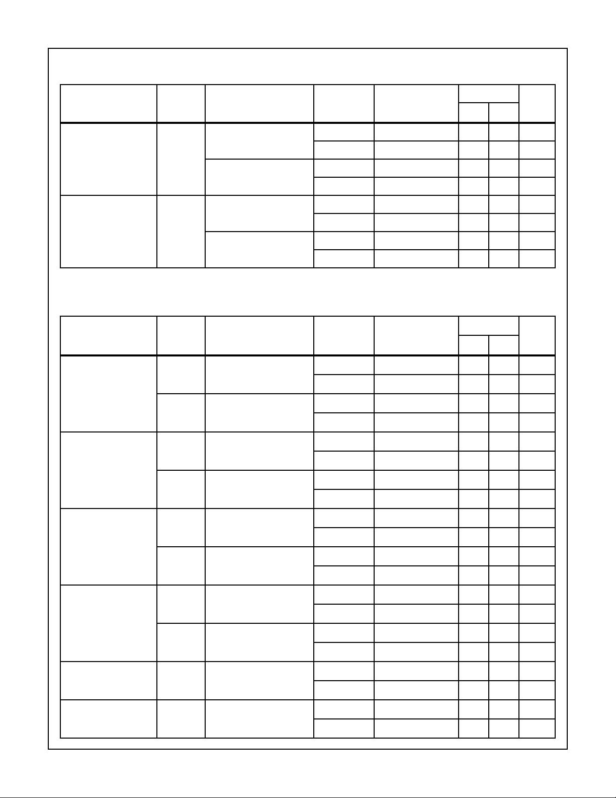
TABLE 1. HS-302RH/303RH/384RH/390RH/883S DC ELECTRICAL PERFORMANCE CHARACTERISTICS
Device Guaranteed and 100% Tested. Unless Otherwise Specified: V- = -15V, V+ = +15V, VAH = +4.0V, VAL = 0.8V (Continued)
GROUP A
SUB-
PARAMETER SYMBOL CONDITIONS
Positive Supply Current I(+) All Channels VA = 0.8V 1 +25oC-10µA
GROUPS TEMPERATURE
2, 3 -55oC to +125oC - 100 µA
LIMITS
UNITSMIN MAX
VA1 = 0V, VA2 = 4.0V and
VA1 = 4.0V, VA2 = 0V
Negative Supply
Current
TABLE 1. HS-306RH/307RH/883S DC ELECTRICAL PERFORMANCE CHARACTERISTICS
Device Guaranteed and 100% Tested. Unless Otherwise Specified: V- = -15V, V+ = +15V, VAH = +11.0V, VAL = 3.5V
PARAMETER SYMBOL CONDITIONS
“Switch On” Resistance +RDS VD = 10V, IS = -10mA,
Leakage Current Into
the Source Terminal of
an “Off” Switch
I(-) All Channels VA = 0.8V 1 +25oC -10 - µA
VA1 = 0V, VA2 = 4.0V and
VA1 = 4.0V, VA2 = 0V
S1/S2/S3/S4
+RDS VD = -10V, IS = 10mA,
S1/S2/S3/S4
+IS(OFF) VS = +14V, VD = -14V,
S1/S2/S3/S4
1 +25oC - 0.5 mA
2, 3 -55oC to +125oC-1mA
2, 3 -55oC to +125oC -100 - µA
1 +25oC -10 - µA
2, 3 -55oC to +125oC -100 - µA
GROUP A
SUB-
GROUPS TEMPERATURE
1 +25oC-50Ω
2, 3 -55oC to +125oC-75Ω
1 +25oC-50Ω
2, 3 -55oC to +125oC-75Ω
1 +25oC-22nA
2, 3 -55oC to +125oC -100 100 nA
LIMITS
UNITSMIN MAX
Leakage Current into
theDrainTerminalofan
“Off” Switch
Leakage Current from
an “On” Driver Into the
Switch (Drain and
Source)
Low Level Input
Address Current
High Level Input
Address Current
-IS(OFF) VS = -14V, VD = +14V,
S1/S2/S3/S4
+ID(OFF) VS = -14V, VD = +14V,
S1/S2/S3/S4
-ID(OFF) VS = +14V, VD = -14V,
S1/S2/S3/S4
+ID(ON) VS = VD = +14V,
S1/S2/S3/S4
-ID(ON) VS = VD = -14V,
S1/S2/S3/S4
IAL All Channels VA = 3.5V 1 +25oC-11µA
IAH All Channels VA = 11V 1 +25oC-11µA
1 +25oC-22nA
2, 3 -55oC to +125oC -100 100 nA
1 +25oC-22nA
2, 3 -55oC to +125oC -100 100 nA
1 +25oC-22nA
2, 3 -55oC to +125oC -100 100 nA
1 +25oC-22nA
2, 3 -55oC to +125oC -100 100 nA
1 +25oC-22nA
2, 3 -55oC to +125oC -100 100 nA
1, 2 -55oC to +125oC-11 µA
1, 2 -55oC to +125oC-11 µA
Spec Number 518526
5
 Loading...