

查询5962F9568901QEC供应商查询5962F9568901QEC供应商
TM
HS-26C32RH
Data Sheet August 2000
Radiation HardenedQuadDifferentialLine
Receiver
The Intersil HS-26C32RH is a differential line receiver
designed for digital data transmission over balanced lines
and meets the requirements of EIA Standard RS-422.
Radiation hardened CMOS processing assures low power
consumption, high speed, and reliable operation in the most
severe radiation environments.
The HS-26C32RHhas an input sensitivity typically of 200mV
over the common mode input voltage range of ±7V. The
receivers are also equipped with input fail safe circuitry,
which causes the outputs to go to a logic “1” when the inputs
are open. Enable and Disable functions are common to all
four receivers.
Specifications for Rad Hard QML devices are controlled
by the Defense Supply Center in Columbus (DSCC). The
SMD numbers listed here must be used when ordering.
Detailed Electrical Specifications for these devices are
contained in SMD 5962-95689. A “hot-link” is provided
on our homepage for downloading.
www.intersil.com/spacedefense/space.asp
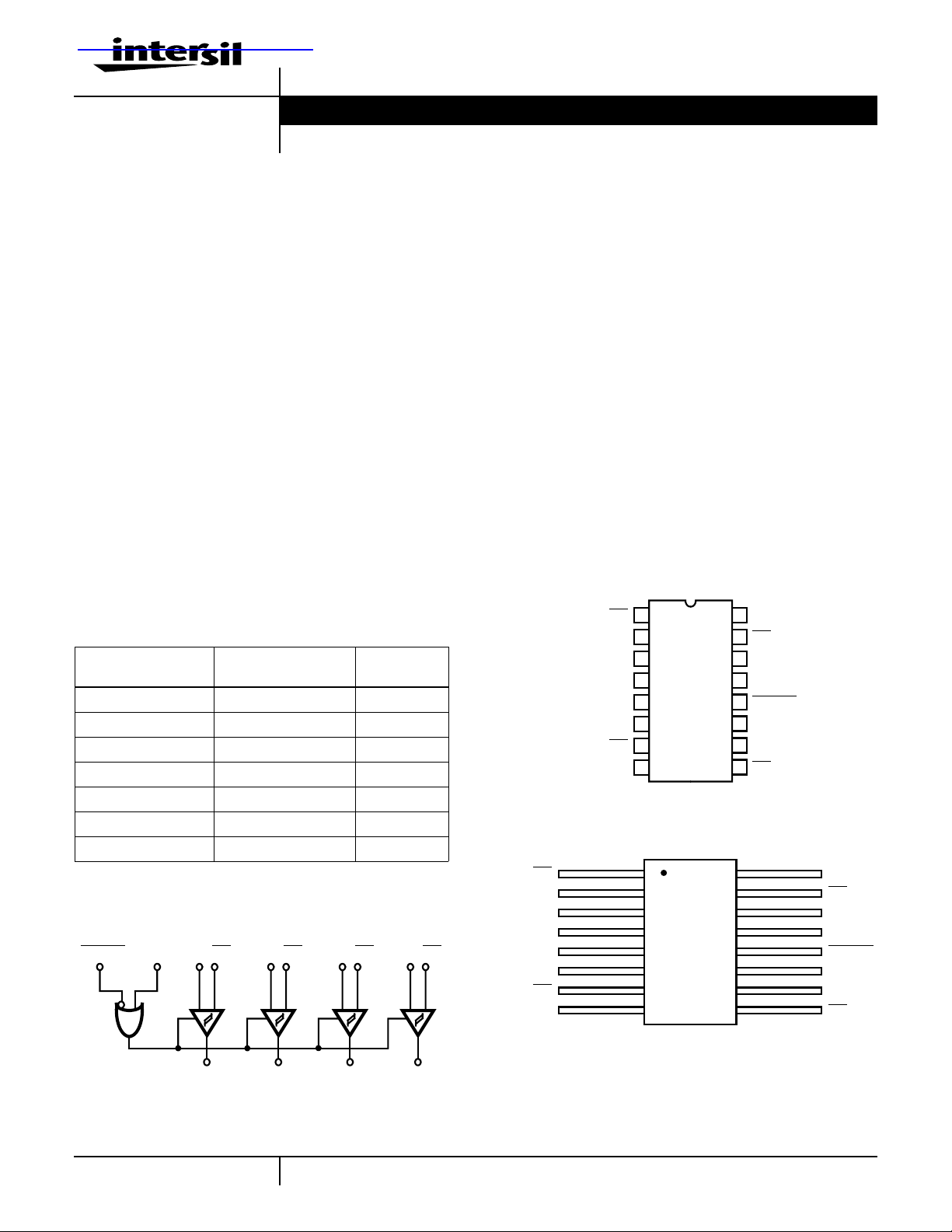
Ordering Information
TEMP. RANGE
ORDERING NO. INTERNAL MKT. NO.
(oC)
5962F9568901QEC HS1-26C32RH-8 -55 to 125
5962F9568901QXC HS9-26C32RH-8 -55 to 125
5962F9568901V9A HS0-26C32RH-Q 25
5962F9568901VEC HS1-26C32RH-Q -55 to 125
5962F9568901VXC HS9-26C32RH-Q -55 to 125
HS1-26C32RH/PROTO HS1-26C32RH/PROTO -55 to 125
HS9-26C32RH/PROTO HS9-26C32RH/PROTO -55 to 125
Logic Diagram
ENABLE ENABLE
DIN CIN CIN BIN BIN AIN AIN
DIN
+-+-+-+-
File Number 3402.3
Features
• Electrically Screened to SMD # 5962-95689
• QML Qualified per MIL-PRF-38535 Requirements
• 1.2 Micron Radiation Hardened CMOS
- Total Dose. . . . . . . . . . . . . . . . . . . . .300 krad(Si) (Max)
• Latchup Free
• EIA RS-422 Compatible Inputs
• CMOS Compatible Outputs
• Input Fail Safe Circuitry
• High Impedance Inputs when Disabled or Powered Down
• Low Power Dissipation 138mW Standby (Max)
• Single 5V Supply
o
• Full -55
C to 125oC Military Temperature Range
Pinouts
HS1-26C32RH 16 LEAD CERAMIC SIDEBRAZE DIP
MIL-STD-1835: CDIP2-T16
TOP VIEW
VDD
16
15
BIN
BIN
14
BOUT
13
12
ENABLE
DOUT
11
10
DIN
9
DIN
VDD
15
14
13
12
11
10
9
BIN
BIN
BOUT
ENABLE
DOUT
DIN
DIN
AIN
AIN
AOUT
ENABLE
COUT
CIN
CIN
GND
1
AIN
2
AIN
3
AOUT
COUT
CIN
CIN
GND
4
5
6
7
8
ENABLE
HS9-26C32RH 16 LEAD FLATPACK
MIL-STD-1835: CDFP4-F16
TOP VIEW
116
2
3
4
5
6
7
8
DOUT
AOUTBOUTCOUT
1
1-888-INTERSIL or 321-724-7143 | Intersil and Design is a trademark of Intersil Corporation. | Copyright © Intersil Corporation 2000
CAUTION: These devices are sensitive to electrostatic discharge; follow proper IC Handling Procedures.
HS-26C32RH
Propagation Delay Timing Diagram
-V
IN
+VIN = 0V
V
OH
V
OL
INPUT
t
PLH
VS = 50%
0V
t
PHL
OUTPUT
Three-State Low Timing Diagram
V
IH
V
S
V
SS
V
OZ
V
OL
INPUT
T
PZL
V
T
T
OUTPUT
PLZ
Propagation Delay Load Circuit
TEST
POINT
R
L
+2.5V
-2.5V
DUT
= 50pF
C
L
= 1000Ω
R
L
C
L
Three-State High Timing Diagrams
V
IH
t
PZH
INPUT
V
T
t
OUTPUT
PHZ
V
W
V
S
V
SS
V
OH
V
W
V
OZ
THREE-STATE LOW VOLTAGE LEVELS
PARAMETER HS-26C32RH UNITS
V
DD
V
IH
V
S
V
T
V
W
4.50 V
4.50 V
2.25 V
50 %
VOL + 0.5 V
GND 0 V
Three-State Low Load Circuit
V
DD
R
L
TEST
POINT
C
L
C
= 50pF
L
= 1000Ω
R
L
DUT
THREE-STATE HIGH VOLTAGE LEVELS
PARAMETER HS-26C32RH UNITS
V
DD
V
IH
V
S
V
T
V
W
4.50 V
4.50 V
2.25 V
50 %
VOH - 0.5 V
GND 0 V
Three-State High Load Circuit
DUT
C
L
= 50pF
C
L
RL = 1000Ω
TEST
POINT
R
L
2
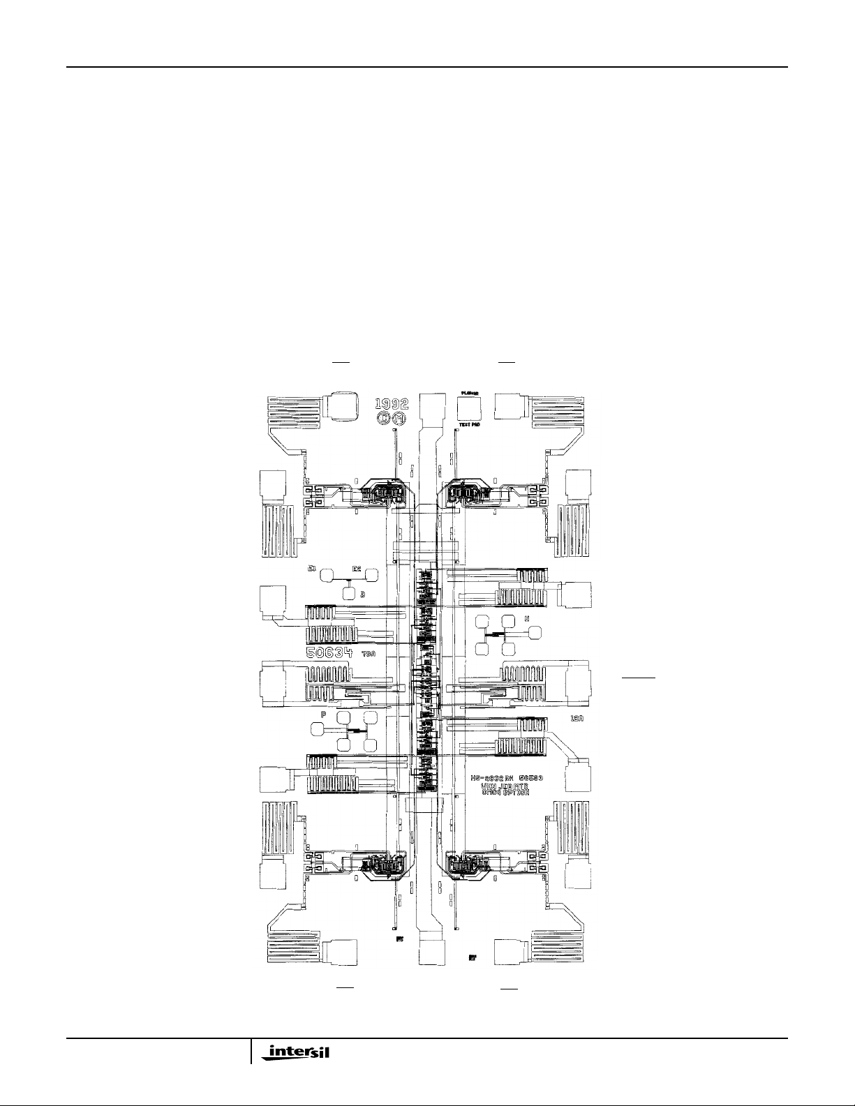
Die Characteristics
HS-26C32RH
DIE DIMENSIONS:
84 mils x 130 mils
(2140µm x 3290µm)
INTERFACE MATERIALS:
Glassivation:
Type: SiO
2
Thickness: 10kű 1kÅ
Metallization Mask Layout
AIN (2)
Top Metallization:
M1: Mo/Tiw
Thickness: 5800Å
M2: Al/Si/Cu
Thickness: 5800
Worst Case Current Density:
<2.0 x 10
Bond Pad Size:
110µm x 100µm
HS-26C32RH
AIN V
(1) (16) (15)
DD
BIN
5
A/cm
Å
2
(14) B
IN
A
(3)
OUT
ENAB (4)
C
(5)
OUT
(6)
C
IN
(7)
CIN
(8) (9)
GND
DIN
(13) B
OUT
(12) ENAB
(11) D
OUT
(10) D
IN
3
HS-26C32RH
All Intersil semiconductor products are manufactured, assembled and tested under ISO9000 quality systems certification.
Intersil semiconductor products are sold by description only. Intersil Corporation reserves the right to make changes in circuit design and/or specifications at any time without notice. Accordingly , the reader is cautioned to verify that data sheets are current before placing orders. Information furnished by Intersil is believed to be accurate and
reliable. However, no responsibility is assumed by Intersil or its subsidiaries for its use; nor for any infringements of patents or other rights of third parties which may result
from its use. No license is granted by implication or otherwise under any patent or patent rights of Intersil or its subsidiaries.
For information regarding Intersil Corporation and its products,see web site www.intersil.com
Sales Office Headquarters
NORTH AMERICA
Intersil Corporation
P. O. Box 883, Mail Stop 53-204
Melbourne, FL 32902
TEL: (321) 724-7000
FAX: (321) 724-7240
4
EUROPE
Intersil SA
Mercure Center
100, Rue de la Fusee
1130 Brussels, Belgium
TEL: (32) 2.724.2111
FAX: (32) 2.724.22.05
ASIA
Intersil Ltd.
8F-2, 96, Sec. 1, Chien-kuo North,
Taipei, Taiwan 104
Republic of China
TEL: 886-2-2515-8508
FAX: 886-2-2515-8369
 Loading...