Intersil Corporation HS-26C32RH Datasheet

August 1995
HS-26C32RH
Radiation Hardened
Quad Differential Line Receiver
Features
• 1.2 Micron Radiation Hardened CMOS
- Total Dose Up to 300K RAD (Si)
• Latchup Free
• EIA RS-422 Compatible Outputs
• CMOS Compatible Inputs
• Input Fail Safe Circuitry
• High Impedance Inputs when Disabled or Powered
Down
• Low Power Dissipation 138mW Standby (Max)
• Single 5V Supply
o
• Full -55
C to +125oC Military Temperature Range
Description
The Intersil HS-26C32RH is a differential line receiver
designed for digital data transmission over balanced lines
and meets the requirements of EIA standard RS-422.
Radiation hardened CMOS processing assures low power
consumption, high speed, and reliable operation in the most
severe radiation environments.
The HS-26C32RH has an input sensitivity typically of 200mV
over the common mode input voltage range of ±7V. The
receivers are also equipped with input fail safe circuitry, which
causes the outputs to go to a logic “1” when the inputs are
open. Enable and Disable functions are common to all four
Pinouts
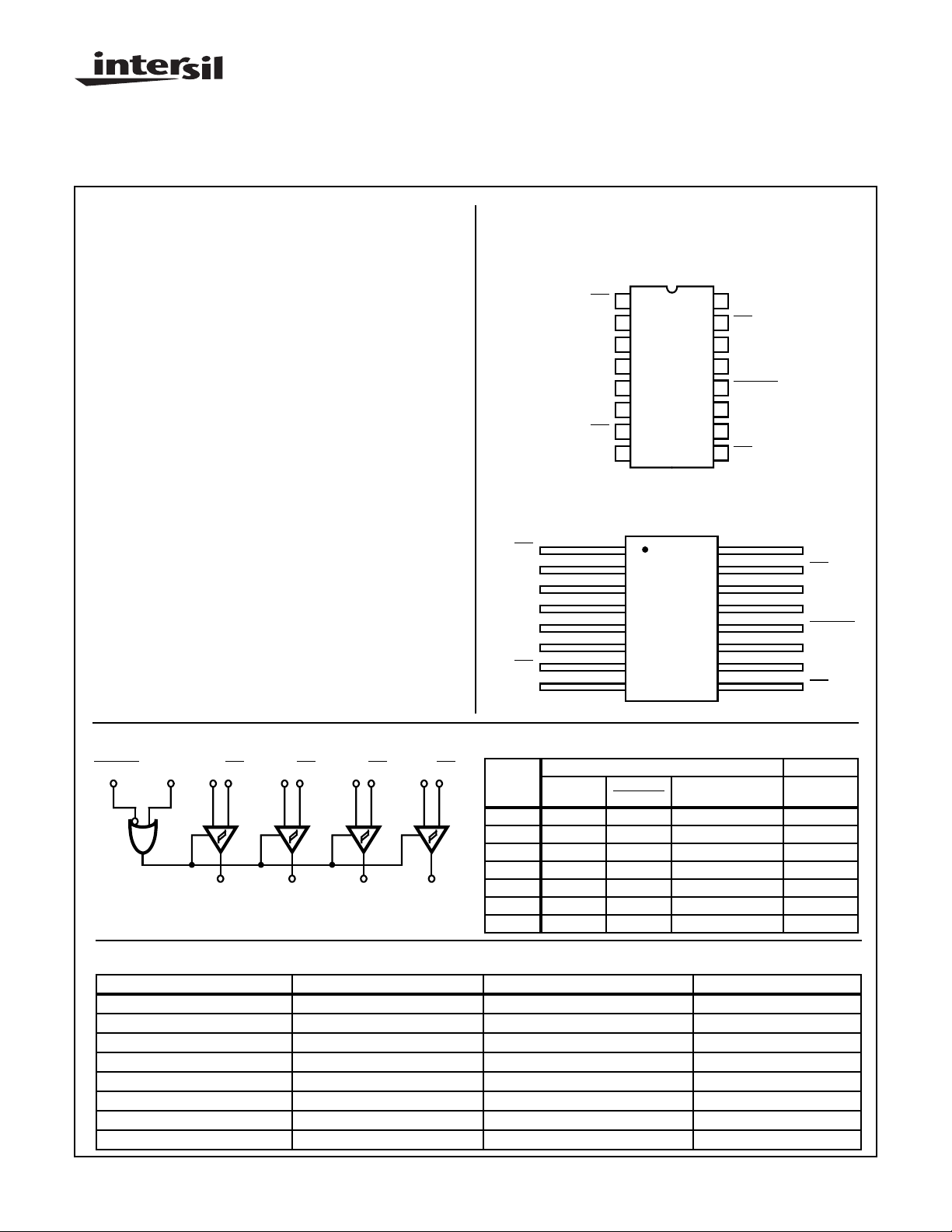
HS1-26C32RH 16 LEAD CERAMIC SIDEBRAZE DIP
MIL-STD-1835: CDIP2-T16
TOP VIEW
VDD
16
15
BIN
BIN
14
BOUT
13
12
ENABLE
DOUT
11
10
DIN
9
DIN
15
14
13
12
11
10
9
AIN
AIN
AOUT
ENABLE
COUT
CIN
CIN
GND
1
AIN
2
AIN
3
AOUT
ENABLE
HS9-26C32RH 16 LEAD FLATPACK
4
5
COUT
6
CIN
7
CIN
8
GND
MIL-STD-1835: CDFP4-F16
TOP VIEW
116
2
3
4
5
6
7
8
VDD
BIN
BIN
BOUT
ENABLE
DOUT
DIN
DIN
Logic Diagram
ENABLE ENABLE
DIN
DOUT
DIN CIN CIN BIN BIN AIN AIN
+-+-+-+-
AOUTBOUTCOUT
DEVICE
POWER
ON/OFF
ENABLE ENABLE INPUT OUT
ON 0 1 X HI-Z
ON 1 X VID ≥VTH (Max) 1
ON 1 X VID ≤VTH (Min) 0
ON X 0 VID ≥ VTH (Max) 1
ON X 0 VID ≤ VTH (Min) 0
ON 1 X Open 1
ON X 0 Open 1
TRUTH TABLE
INPUTS OUTPUT
Ordering Information
PART NUMBER TEMPERATURE RANGE SCREENING LEVEL PACKAGE
HS1-26C32RH-8 -55oC to +125oC Intersil Class B Equivalent 16 Lead Sideboard DIP
HS1-26C32RH-Q -55oC to +125oC Intersil Class S Equivalent 16 Lead Sideboard DIP
HS9-26C32RH-8 -55oC to +125oC Intersil Class B Equivalent 16 Lead Flatpack
HS9-26C32RH-Q -55oC to +125oC Intersil Class S Equivalent 16 Lead Flatpack
HS1-26C32RH/Sample +25oC Sample 16 Lead Sideboard DIP
HS1-26C32RH/Proto -55oC to +125oC Prototype 16 Lead Sideboard DIP
HS9-26C32RH/Sample +25oC Sample 16 Lead Flatpack
HS9-26C32RH/Proto -55oC to +125oC Prototype 16 Lead Flatpack
CAUTION: These devices are sensitive to electrostatic discharge; follow proper IC Handling Procedures.
407-727-9207
| Copyright © Intersil Corporation 1999
774
Spec Number
File Number 3402.2
DB NA
518790

Specifications HS-26C32RH
Absolute Maximum Ratings Reliability Information
Supply Voltage . . . . . . . . . . . . . . . . . . . . . . . . . . . . . .-0.5V to +7.0V
Differential Input Voltage. . . . . . . . . . . . . . . . . . . . . . . . . . . . . . . . . ±12V
Common Mode Range . . . . . . . . . . . . . . . . . . . . . . . . . . . . . . . . . . ±12V
Enable Pins Input Voltage . . . . . . . . . . . . . . . . . -0.5V to VDD+0.5V
DC Drain Current (Any One Output). . . . . . . . . . . . . . . . . . . . . .±25mA
DC Diode Input Current Enable Pin . . . . . . . . . . . . . . . . . . . . . . . ±1µA
Storage Temperature Range . . . . . . . . . . . . . . . . . -65oC to +150oC
Lead Temperature (Soldering 10s). . . . . . . . . . . . . . . . . . . . +300oC
ESD Classification . . . . . . . . . . . . . . . . . . . . . . . . . . . . . . . . Class 1
CAUTION: Stresses above those listed in “Absolute Maximum Ratings” may cause permanent damage to the device. This is a stress only rating and operation
of the device at these or any other conditions above those indicated in the operational sections of this specification is not implied.
Operating Conditions
Operating Voltage Range. . . . . . . . . . . . . . . . . . . . . +4.5V to +5.5V
Operating Temperature Range. . . . . . . . . . . . . . . . -55oC to +125oC
Common Mode Range . . . . . . . . . . . . . . . . . . . . . . . . . . . . . . . . . .±7.0V
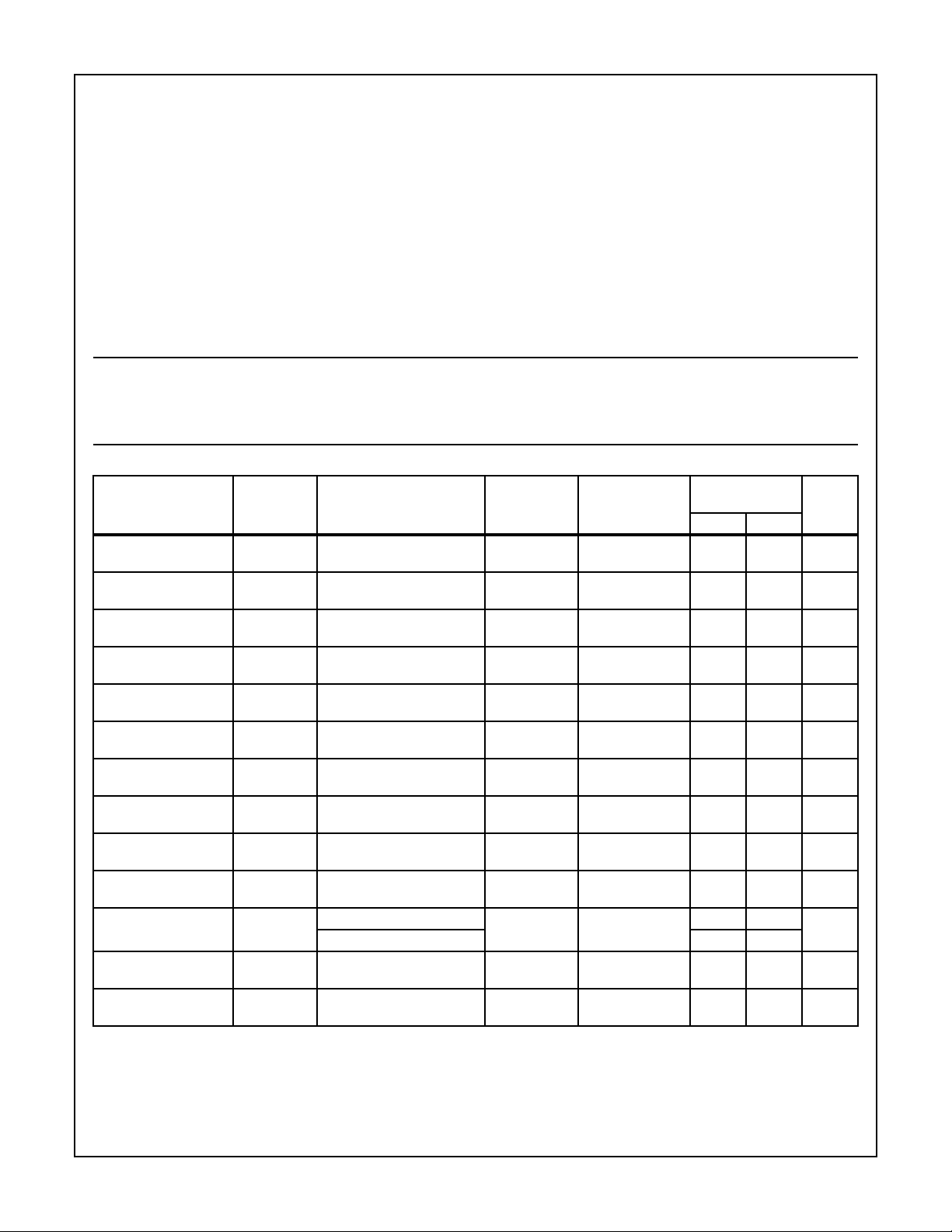
TABLE 1. DC ELECTRICAL PERFORMANCE CHARACTERISTICS
(NOTE 1)
PARAMETER SYMBOL
High Level Output
Voltage
Low Level Output
Voltage
Differential Input
Voltage
Enabled High Level
Input Voltage
Enabled Low Level
Input Voltage
Input Current High
(Differential Inputs)
Input Current Low
(Differential Inputs)
Input Leakage Enable
Pins
Three-State Output
Leakage Current
Standby Supply
Current
Enable Clamp Voltage VIC At -1mA 1, 2, 3 -55oC, +25oC,
Input Hysteresis VHYST 1 -55oC, +25oC,
Input Resistance RIN -7V ≤ VCM ≤ 7V 1 -55oC, +25oC,
NOTES:
1. All voltages referenced to device ground.
2. Force/Measure functions may be interchanged.
3. These test condition are detailed in EIA specification RS-422.
4. This parameter tested as inputs for the VOL, VOH, IOZ tests.
5. VIL = 0.3VDD, VIH = 0.7VDD.
VOH VDD = 4.5V, VDIFF = 1.0V,
VOL VDD = 4.5V, VDIFF = -1.0V,
VTH VDD = VIH = 4.5V,
VIH VDD = 4.5V, 5.5V (Note 4) 1, 2, 3 -55oC, +25oC,
VIL VDD = 4.5V, 5.5V (Note 4) 1, 2, 3 -55oC, +25oC,
IINH VDD = 5.5, +V = 10V, -V =
IINL VDD = 5.5, +V = -10V, -V =
IIN VDD = 5.5V, VIN = 0V, 5.5V 1, 2, 3 -55oC, +25oC,
IOZ VDD = 5.5V, VO = VDD or
IDDSB VDD = 5.5V, VDIFF = 1.0V
CONDITIONS
IO = -6mA (Notes 2, 5)
IO = 6mA (Note 5)
-7.0V < VCM < 7.0V
0V and +V = 0V, -V = 10V
0V and +V = 0V, -V = -10V
GND
Outputs = Open
At 1mA - 1.5
Thermal Resistance θ
SBDIP Package. . . . . . . . . . . . . . . . . . . . 80oC/W 20oC/W
Ceramic Flatpack Package . . . . . . . . . . . 103oC/W 26oC/W
Maximum Package Power Dissipation at +125oC
SBDIP Package. . . . . . . . . . . . . . . . . . . . . . . . . . . . . . . . . . . 0.6W
Ceramic Flatpack Package . . . . . . . . . . . . . . . . . . . . . . . . . . 0.5W
Maximum Device Power Dissipation. . . . . . . . . . . . . . . . . . . . . 0.3W
Note: Maximum device Power Dissipation is defined as VDD x ICC
and must withstand the added PD due to output current test; IO at
+125oC
Derating Requirements:
SBDIP Package. . . . . . . . . . . . . . . . . . . . . .No Derating Required
Ceramic Flatpack Package . . . . . . . . . . . . .No Derating Required
Input Low Voltage (VIL). . . . . . . . . . . . . . . . . . . . 0V to 0.3VDD Max
Input High Voltage (VIH). . . . . . . . . . . . . . . . . . VDD to 0.7VDD Min
Input Rise and Fall Time. . . . . . . . . . . . . . . . . . . . . . . . . 500ns Max
GROUP A
SUBGROUPS TEMPERATURE
1, 2, 3 -55oC, +25oC,
+125oC
1, 2, 3 -55oC, +25oC,
+125oC
1, 2, 3 -55oC, +25oC,
+125oC
+125oC
+125oC
1, 2, 3 -55oC, +25oC,
+125oC
1, 2, 3 -55oC, +25oC,
+125oC
+125oC
1, 2, 3 -55oC, +25oC,
+125oC
1, 2, 3 -55oC, +25oC,
+125oC
+125oC
+125oC
+125oC
4.1 - V
-400 +400 mV
0.7
VDD
-5.0 5.0 µA
20 100 mV
420kΩ
JA
(NOTE 2)
LIMITS
- 0.4 V
-V
- 0.3
VDD
- 1.8 mA
- -2.7 mA
- ±1.0 µA
-25mA
- -1.5 V
θ
JC
UNITSMIN MAX
V
775
Spec Number 518790

Specifications HS-26C32RH
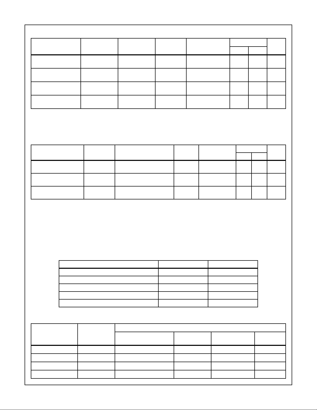
TABLE 2. AC ELECTRICAL PERFORMANCE CHARACTERISTICS
(NOTES 1, 2)
PARAMETER SYMBOL
Propagation Delay Time TPLH, TPHL VDD = 4.5V,
Propagation Delay Time TPZH, TPZL VDD = 4.5V,
Propagation Delay Time TPLZ, TPHZ VDD = 4.5V,
Propagation Delay Time
TRISE/TFALL
NOTES:
1. All voltages referenced to device ground.
2. See Table EIA RS-422
PARAMETER SYMBOL
Input Capacitance CIN VDD = Open, f = 1MHz 1 -55oC, +25oC,
Output Capacitance COUT VDD = Open, f = 1MHz 1 -55oC, +25oC,
Fail Safe FSAFE + and - Inputs are Open,
NOTE:
1. The parameters listed on Table 3 are controlled via design or process parameters. Min and Max limits are guaranteed but not directly
tested. These parameters are characterized at initial design release and upon design changes which would affect these characteristics.
TTHL, TTLH VDD = 4.5V,
TABLE 3. ELECTRICAL PERFORMANCE CHARACTERISTICS
CONDITIONS
VDIFF = 2.5V
VDIFF = 2.5V
VDIFF = 2.5V
VDIFF = 2.5V
(NOTE 1)
CONDITIONS NOTES TEMPERATURE
VOUT = Logic “1”
GROUP A
SUBGROUPS TEMPERATURE
9, 10, 11 -55oC, +25oC,
+125oC
9, 10, 11 -55oC, +25oC,
+125oC
9, 10, 11 -55oC, +25oC,
+125oC
9, 10, 11 -55oC, +25oC,
+125oC
+125oC
+125oC
1 -55oC, +25oC,
+125oC
LIMITS
UNITSMIN MAX
640ns
318ns
629ns
212ns
LIMITS
UNITSMIN MAX
-12pF
-12pF
4.1 - V
TABLE 4. POST IRRADIATION ELECTRICAL PERFORMANCE CHARACTERISTICS
The post irradiation electrical performance characteristics are the same as the parameters listed in Tables 1, 2 and 3.
TABLE 5. BURN-IN DELTA PARAMETERS (+25oC) AND GROUP B, SUBGROUP 5 DELTA PARAMETERS
PARAMETER SYMBOL DELTA LIMITS
Standby Supply Current IDDSB ±4mA
Three-State Output Leakage Current IOZ ±1.0µA
Low Level Output Voltage VOL ±60mV
High Level Output Voltage VOH ±150mV
Input Leakage Current IIN ±150nA
TABLE 6. APPLICABLE SUBGROUPS
GROUP A SUBGROUPS
CONFORMANCE
GROUP
Initial Test 100% 5004 1, 7, 9 1 (Note 2) 1, 7, 9
Interim Test 100% 5004 1, 7, 9, ∆ 1, ∆(Note 2) 1, 7, 9
PDA 1 & 2 100% 5004 1, 7, ∆ - 1, 7
Final Test 100% 5004 2, 3, 8A, 8B, 10, 11 - 2, 3, 8A, 8B, 10, 11
MIL-STD-883
METHOD
TESTED FOR -Q
RECORDED
FOR -Q TESTED FOR -8
RECORDED
FOR -8
776
Spec Number 518790
 Loading...