Intersil Corporation HS-2420RH Datasheet

July 1995
HS-2420RH
Radiation Hardened
Fast Sample and Hold
Features
• Maximum Acquisition Time
- 10V Step to 0.1%. . . . . . . . . . . . . . . . . . . . . . . . . . . 4µs
- 10V Step to 0.01%. . . . . . . . . . . . . . . . . . . . . . . . . . 6µs
• Maximum Drift Current . . . . . . . . . . . . . . . . . . . . . .10nA
(Maximum Over Temperature)
• TTL Compatible Control Input
• Power Supply Rejection . . . . . . . . . . . . . . . . . . . . . .≥80dB
5
• Total Gamma Dose. . . . . . . . . . . . . . . . .1 x 10
RAD(SI)
• No Latch-Up
Applications
• Data Acquisition Systems
• D to A Deglitcher
• Auto Zero Systems
• Peak Detector
• Gated Op Amp
Ordering Information
Description
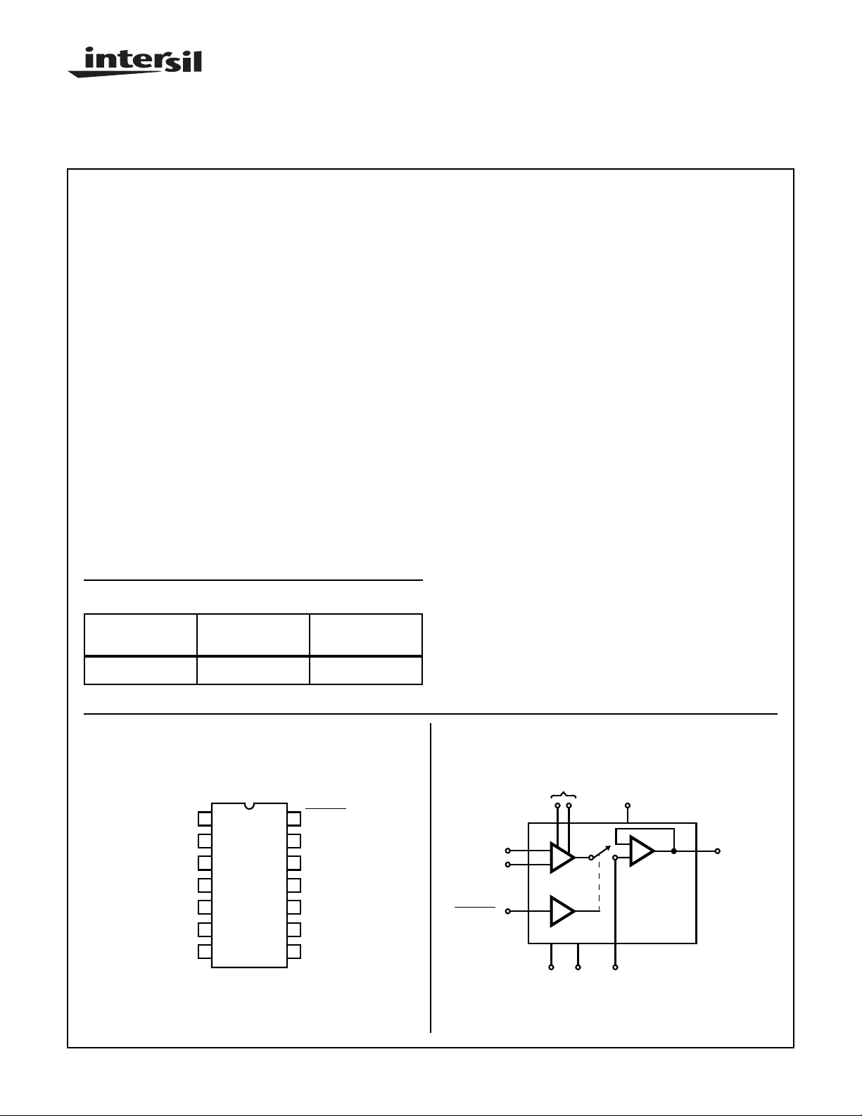
The HS-2420RH is a radiation hardened monolithic circuit
consisting of a high performance operational amplifier with
its output in series with an ultra-low leakage analog switch
and MOSFET input unity gain amplifier.
With an external hold capacitor connected to the switch output,
a versatile, high performance sample-and-hold or track-andhold circuit is formed. When the switch is closed, the device
behaves as an operation amplifier, and any of the standard op
amp feedback networks may be connected around the device
to control gain, frequency response, etc. When the switch is
opened the output will remain at its last level.
Performance as a sample-and-hold compares very favorably
with other monolithic, hybrid, modular, and discrete circuits.
Accuracy to better than 0.01% is achievable over the
temperature range. Fast acquisition is coupled with superior
droop characteristics, even at high temperatures. High slew
rate, wide bandwidth, and low acquisition time produce
excellent dynamic characteristics. The ability to operate at
gains greater than 1 frequently eliminates the need for
external scaling amplifiers.
The device may also be used as a versatile operational
amplifier with a gated output for applications such as analog
switches, peak holding circuits, etc.
TEMPERATURE
PART NUMBER
HS1-2420RH-Q -55oC to +125oC 14 Lead CerDIP
Pinout
OFFSET ADJUST
OFFSET ADJUST
14 LEAD CERAMIC DUAL-IN-LINE
FRIT SEAL PACKAGE (CerDIP)
MIL-STD-1835, GDIP1-T14
IN-
IN+
V-
NC
OUTPUT
RANGE PACKAGE
TOP VIEW
1
2
3
4
5
6
7
14 Pin DIP
SAMPLE/HOLD
14
CONTROL
13
GND
12
NC
11
HOLD CAPACITOR
10
NC
9
V+
8
NC
Functional Diagram
OFFSET
ADJUST
34 5
HOLD
1
2
14
-
+
V-GND
- INPUT
+ INPUT
SAMPLE/
CONTROL
NOTE: Pin Numbers Correspond to DIP Package Only.
V+
513
11
HOLD
CAPACITOR
-
+
HS-2420RH
7
OUTPUT
CAUTION: These devices are sensitive to electrostatic discharge; follow proper IC Handling Procedures.
http://www.intersil.com
| Copyright © Intersil Corporation 1999
1
Spec Number 518855
File Number 3554.1

Specifications HS-2420RH
Absolute Maximum Ratings Reliability Information
Voltage Between V+ and V- Terminals. . . . . . . . . . . . . . . . . . . +40V
Differential Input Voltage. . . . . . . . . . . . . . . . . . . . . . . . . . . . . . . . . ±24V
Digital Input Voltage (S/H Pin) . . . . . . . . . . . . . . . . . . . . . .+8V, -15V
Output Current . . . . . . . . . . . . . . . . . . . . . . . Short Circuit Protected
Storage Temperature Range . . . . . . . . . . . . . .-65oC < TA < +150oC
Lead Temperature (Soldering 10s). . . . . . . . . . . . . . . . . . . . +275oC
Junction Temperature. . . . . . . . . . . . . . . . . . . . . . . . . . . . . . +175oC
CAUTION: Stresses above those listed in “Absolute Maximum Ratings” may cause permanent damage to the device. This is a stress only rating and operation
of the device at these or any other conditions above those indicated in the operational sections of this specification is not implied.
Recommended Operating Conditions
Operating Temperature Range. . . . . . . . . . . . .-55oC < TA < +125oC
Operating Supply Voltage (±VSUPPLY) . . . . . . . . . . . . . . . . . . . ±15V
Analog Input Voltage (VS) . . . . . . . . . . . . . . . . . . . . . . . . . . . . . . . ±10V
TABLE 1. DC ELECTRICAL PERFORMANCE CHARACTERISTICS
Device T ested at V+ = +15V, V - = -15V, VIL = 0.8V (Sample); VIH = 2.0V (Hold); CH = 1000pF, -Input Tied to Output, Unless Otherwise Specified
PARAMETER SYMBOL CONDITIONS
Input Offset Voltage VIO 1 +25oC-44mV
Input Bias Current IB+ 1 +25oC -200 200 nA
IB- 1 +25oC -200 200 nA
Input Offset Current IIO 1 +25oC -50 50 nA
Open Loop Voltage Gain +AVS RL = 2kΩ, CL = 50pF,
VOUT = +10V
-AVS RL = 2kΩ, CL = 50pF,
VOUT = -10V
Common Mode
Rejection Ratio
Output Current +IO VOUT = +10V 1 +25oC +15.0 - mA
Output Voltage Swing +VOP RL = 2kΩ, CL = 50pF 1 +25oC +10.0 - V
Power Supply Current +ICC 1 +25oC - 5.5 mA
Power Supply Rejection
Ratio
-CMRR V+ = 25V, V- = -5V,
VOUT = +10V, VS/H = 10.8V
+CMRR V+ = 5V, V- = -25V,
VOUT = -10V, VS/H = 9.2V
-IO VOUT = -10V 1 +25oC -15.0 - mA
-VOP RL = 2kΩ, CL = 50pF 1 +25oC - -10.0 V
-ICC 1 +25oC -3.5 - mA
+PSRR V+ = 10V and 20V,
V- = -15V and -15V
-PSRR V+ = 15V and 15V,
V- = -10V and -20V
Thermal Resistance θ
CerDIP Package . . . . . . . . . . . . . . . . . . . 74oC/W 18oC/W
Maximum Power Dissipation at +125oC
CerDIP Package . . . . . . . . . . . . . . . . . . . . . . . . . . . . . . . . .0.68W
If Device Power Exceeds Package Dissipation Capability, Derate
Linearly at the Following Rate
CerDIP Package . . . . . . . . . . . . . . . . . . . . . . . . . . . . .13.5mW/oC
ESD Classification . . . . . . . . . . . . . . . . . . . . . . . . . . . . . . . . . . . ≤2000V
Logic Level Low (VIL) . . . . . . . . . . . . . . . . . . . . . . . . . . . .0V to 0.8V
Logic Level High (VIH) . . . . . . . . . . . . . . . . . . . . . . . . . 2.0V to 5.0V
GROUP A
SUBGROUPS TEMPERATURE
2, 3 -55oC, +125oC-6 6 mV
2, 3 -55oC, +125oC -400 400 nA
2, 3 -55oC, +125oC -400 400 nA
2, 3 -55oC, +125oC -100 100 nA
1 +25oC 25 - kV/V
2, 3 -55oC, +125oC 25 - kV/V
1 +25oC 25 - kV/V
2, 3 -55oC, +125oC 25 - kV/V
1 +25oC80-dB
2, 3 -55oC, +125oC80 - dB
1 +25oC80-dB
2, 3 -55oC, +125oC80 - dB
2, 3 -55oC, +125oC -10.0 - V
2, 3 -55oC, +125oC - -10.0 V
1 +25oC80-dB
2, 3 -55oC, +125oC80 - dB
1 +25oC80-dB
2, 3 -55oC, +125oC80 - dB
JA
LIMITS
θ
JC
UNITSMIN MAX
Spec Number 518855
2

Specifications HS-2420RH
TABLE 1. DC ELECTRICAL PERFORMANCE CHARACTERISTICS (Continued)
Device T ested at V+ = +15V, V- = -15V , VIL = 0.8V (Sample); VIH = 2.0V (Hold); CH = 1000pF, -Input Tied to Output, Unless Otherwise Specified
GROUP A
PARAMETER SYMBOL CONDITIONS
Digital Input Current IIN1 VIN1 = 0V 1 +25oC - 800 µA
IIN2 VIN2 = 5.0V 1 +25oC-20µA
Digital Input Voltage VIL 1 +25oC - 0.8 V
VIH 1 +25oC 2.0 - V
Drift Current ID VIN = 0V, RL = 2kΩ, CL = 50pF,
S/H = 4.0V
TABLE 2. AC ELECTRICAL PERFORMANCE CHARACTERISTICS
Device Tested at V+ = +15V, V- = -15V, VIL = 0.8V (Sample), VIH = 2.0V (Hold), CH = 1000pF , -Input Tied to Output, Unless Otherwise Specified
PARAMETER SYMBOL CONDITIONS
Hold Step Error VERROR VS/H = 0V and 4V,
tRISE (VS/H) ≈30ns (Note 1)
Transient Response
Rise Time and Fall Time
Transient Response
Overshoot
Transient Response
Slew Rate
NOTE:
1. VERROR = VOUT (VS/H = 0V) - VOUT (VS/H = 4V)
TR(TR) CL = 50pF, RL = 2kΩ, AV = +1,
TR(TF) 9 +25oC - 100 ns
TR(+OS) CL = 50pF, RL = 2kΩ, AV = +1,
TR(-OS) 9 +25oC - 40 %
TR(+SR) CL = 50pF, RL = 2kΩ, AV = +1,
TR(-SR) 9 +25oC 3.5 - V/µs
VOUT = 200mVP-P
VOUT = 200mVP-P
VOUT = 10VP-P
SUBGROUPS TEMPERATURE
2, 3 -55oC, +125oC - 800 µA
2, 3 -55oC, +125oC-20µA
2, 3 -55oC, +125oC - 0.8 V
2, 3 -55oC, +125oC 2.0 - V
2 +125oC -10 10 nA
GROUP A
SUBGROUP TEMPERATURE
9 +25oC -20 20 mV
9 +25oC - 100 ns
9 +25oC - 40 %
9 +25oC 3.5 - V/µs
LIMITS
UNITSMIN MAX
LIMITS
UNITSMIN MAX
TABLE 3. ELECTRICAL PERFORMANCE CHARACTERISTICS
Device Tested at V+ = +15V, V- = -15V, VIL = 0.8V (Sample), VIH = 2.0V (Hold), CH = 1000pF , -Input Tied to Output, Unless Otherwise Specified
LIMITS
PARAMETER SYMBOL CONDITIONS NOTE TEMPERATURE
Hold Mode Feedthrough
Attenuation
Gain Bandwidth Product GBWP RL = 2kΩ, CL = 50pF, AV = +1,
Acquisition Time (0.1%) +tACQ (0.1%) RL = 2kΩ, CL = 50pF, AV = +1,
Acquisition Time (0.01%) +tACQ (0.01%) RL = 2kΩ, CL = 50pF, AV = +1,
NOTE: 1. Parameters listed in Table 3 are controlled via design or process parameters and are not directly tested at final production. These
parameters are characterized upon initial design release and upon design changes which would affect these characteristics.
VATTEN RL = 2kΩ, CL = 50pF, AV = +1,
VIN = 20VP-P, fIN = 50kHz
VIN = 100mVP-P
VOUT = 0V and +10V
-tACQ (0.1%) RL = 2kΩ, CL = 50pF, AV = +1,
VOUT = 0V and -10V
VOUT = 0V and +10V
-tACQ (0.01%) RL = 2kΩ, CL = 50pF, AV = +1,
VOUT = 0V and -10V
1 +25oC, -55oC,
+125oC
1 +25oC 2.5 - MHz
1 +25oC-4µs
1 +25oC-4µs
1 +25oC-6µs
1 +25oC-6µs
70 - dB
UNITSMIN MAX
Spec Number 518855
3

Specifications HS-2420RH
TABLE 4. DC ELECTRICAL PERFORMANCE CHARACTERISTICS POST 100KRAD
Device T ested at V+ = +15V, V- = -15V , VIL = 0.8V (Sample); VIH = 2.0V (Hold); CH = 1000pF, -Input Tied to Output, Unless Otherwise Specified
GROUP A
PARAMETER SYMBOL CONDITIONS
Input Offset Voltage VIO 1 +25oC-66mV
Input Bias Current IB+ 1 +25oC -400 400 nA
IB- 1 +25oC -400 400 nA
Input Offset Current IIO 1 +25oC -100 100 nA
Open Loop Voltage Gain +AVS RL = 2kΩ, CL = 50pF,
VOUT = +10V
-AVS RL = 2kΩ, CL = 50pF,
VOUT = -10V
Common Mode
Rejection Ratio
Output Current +IO VOUT = +10V 1 +25oC +12.0 - mA
Output Voltage Swing +VOP RL = 2kΩ, CL = 50pF 1 +25oC +10.0 - V
Power Supply Current +ICC 1 +25oC - 5.5 mA
Power Supply Rejection
Ratio
Digital Input Current IIN1 VIN1 = 0V 1 +25oC - 800 µA
Digital Input Voltage VIL 1 +25oC - 0.8 V
Drift Current ID VIN = 0V, RL = 2kΩ, CL = 50pF,
-CMRR V+ = 25V, V- = -5V,
VOUT = +10V, VS/H = 10.8V
+CMRR V+ = 5V, V- = -25V,
VOUT = -10V, VS/H = 9.2V
-IO VOUT = -10V 1 +25oC -12.0 - mA
-VOP RL = 2kΩ, CL = 50pF 1 +25oC - -10.0 V
-ICC 1 +25oC -3.5 - mA
+PSRR V+ = 10V and 20V,
V- = -15V and -15V
-PSRR V+ = 15V and 15V,
V- = -10V and -20V
IIN2 VIN2 = 5.0V 1 +25oC-20µA
VIH 1 +25oC 2.0 - V
S/H = 4.0V
SUBGROUPS TEMPERATURE
1 +25oC 25 - kV/V
2, 3 -55oC, +125oC 25 - kV/V
1 +25oC 25 - kV/V
2, 3 -55oC, +125oC 25 - kV/V
1 +25oC80-dB
2, 3 -55oC, +125oC80 - dB
1 +25oC80-dB
2, 3 -55oC, +125oC80 - dB
2, 3 -55oC, +125oC +10.0 - V
2, 3 -55oC, +125oC - -10.0 V
1 +25oC80-dB
2, 3 -55oC, +125oC80 - dB
1 +25oC80-dB
2, 3 -55oC, +125oC80 - dB
2, 3 -55oC, +125oC - 800 µA
2, 3 -55oC, +125oC-20µA
2, 3 -55oC, +125oC - 0.8 V
2, 3 -55oC, +125oC 2.0 - V
2 +125oC -10 10 nA
LIMITS
UNITSMIN MAX
Spec Number 518855
4
 Loading...