Intersil Corporation HS-1254RH Datasheet

1
PRELIMINARY
April 1998
HS-1254RH
Radiation Hardened, High Speed, Low Power
Dual Operational Amplifier with Disable
Features
• QML Qualified Per MIL-PRF-38535 Requirements
• Radiation Environment
- Total Dose . . . . . . . . . . . . . . . . . . . . .3 x 10
5
RAD(Si)
- SEL Immune . . . . . . . . . . . Bonded Wafer DI Process
• Low Quiescent Current (per amp) . . . . . . 6.1mA (Max)
• Disabled Supply Current (per amp) . . . . . 4.0mA (Max)
• Low Offset Voltage. . . . . . . . . . . . . . . . . . . 5.0mV (Max)
• Output Enable/Disable Time. . . . . . . 160ns/20ns (Typ)
• High Slew Rate . . . . . . . . . . . . . . . . . . . 1050V/µs (Typ)
• Wide -3dB Bandwidth (A
V
= +2) . . . . . . . 530MHz (Typ)
Applications
• High Speed A/D Drivers
• Cable Drivers
• Wideband Signal Switching and Routing
• Redundant Circuit Multiplexing
• Pulse Amplifiers
Description
The HS-1254RH is a ±5V, Rad Hard, monolithic, dual,
current feedback amplifier that provides highly reliable
performance in harsh radiation environments. Dielectric
isolation and bonded wafer processing make this device
immune to latch-up (SEL).
Excellent dynamic characteristics, coupled with the disable
function, make this amplifier well-suited for a variety of satellite system applications. The outputs have individual disable
control pins that make it easy to multiplex wideband signals,
putting the outputs in a high impedance mode and reducing
the supply current per op amp down to 3mA (typical).
Post radiation limits are fully specified and guaranteed to
300kRAD(Si) total dose to ensure predictable performance
in any space application.
Specifications for Rad Hard QML devices are controlled
by the Defense Supply Center in Columbus (DSCC).
SMD numbers must be used when ordering.
Detailed Electrical Specifications for the HS-1254RH are
contained in SMD 5962-98581, which is easily downloadable from our website, via a DSCC “hot-link”.
http://www.semi.intersil.com/data/sm/index.htm
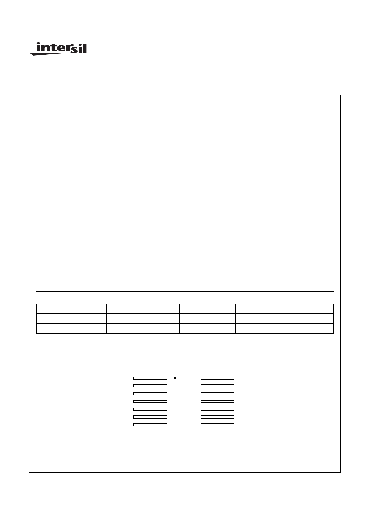
Pinout
HS-1254RH (FLATPACK)
TOP VIEW
Ordering Information
SMD PART NUMBER INTERSIL PART NUMBER TEMP. RANGE (oC) PACKAGE CASE OUTLINE
5962R9858101VXC HS9-1254RH-Q -55 to 125 14 Ld Flatpack CDFP3-F14
N/A HS9-1254RH/Sample 25 14 Ld Flatpack CDFP3-F14
V-
-IN1
+IN1
DISABLE 1
DISABLE 2
+IN2
-IN2
V+
OUT2
OUT1
NC
NC
GND
NC
14
13
12
11
10
9
8
2
3
4
5
6
7
1
File Number 4507
CAUTION: These devices are sensitive to electrostatic discharge; follow proper IC Handling Procedures.
http://www.intersil.com or 407-727-9207
| Copyright © Intersil Corporation 1999

2
Die Characteristics
DIE DIMENSIONS
Size: 1750µm x 2330µm (69 mils x 92 mils)
Thickness: 483µm (19 mils)
GLASSIVATION
Type: Nitride
Thickness: 4k
Å ± 0.5kÅ
METALLIZATION
Metal 1
Type: AlCu(2%)/TiW
Thickness: 8k
Å ± 0.4kÅ
Metal 2
Type: AlCu(2%)
Thickness: 16k
Å ± 0.8kÅ
SUBSTRATE
DI, Bonded Wafer
BACKSIDE FINISH
Silicon
SUBSTRATE POTENTIAL
Floating (Recommend connection to V-)
TRANSISTOR COUNT:
180
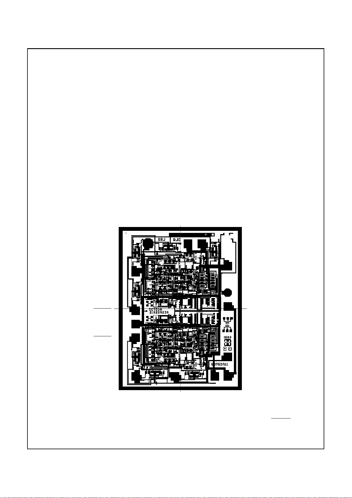
Metallization Mask Layout
HS-1254RH
NOTE:
1. This is an optional GND pad. Users may set a GND reference, via this pad, to ensure the TTL compatibility of the DISABLE inputs when
using asymmetrical supplies (e.g., V+ = 10V, V- = 0V).
-IN1 OUT1
-IN2
GND (SEE NOTE 1)
V-
OUT2
V+
NC
NC
+IN1
+IN2
DISABLE1
DISABLE2
V-
HS-1254RH
 Loading...