Intersil Corporation HS-1145RH Datasheet

HS-1145RH
Data Sheet August 1999
Radiation Hardened, High Speed, Low
Power, Current Feedback Video
Operational Amplifier with Output Disable
The HS-1145RH is a high speed, low power current
feedback amplifier built with Intersil’s proprietary
complementary bipolar UHF-1 (DI bonded wafer) process.
These devices are QML approved and are processed and
screened in full compliance with MIL-PRF-38535.
This amplifier features a TTL/CMOS compatible disable
control, pin 8, which when pulled low, reduces the supply
current and forces the output into a high impedance state.
This allows easy implementation of simple, low power video
switching and routing systems. Component and composite
video systems also benefit from this op amp’s excellent gain
flatness, andgooddifferential gain and phase specifications.
Multiplexed A/D applications will also find the HS-1145RH
useful as the A/D driver/multiplexer.
Specifications for Rad Hard QML devices are controlled
by the Defense Supply Center in Columbus (DSCC). The
SMD numbers listed here must be used when ordering.
Detailed Electrical Specifications for these devices are
contained in SMD 5962-96830. A “hot-link” is provided
on our homepage for downloading.
http://www.intersil.com/spacedefense/space.htm
Ordering Information
INTERNAL
ORDERING NUMBER
5962F9683001VPA HS7-1145RH-Q -55 to 125
5962F9683001VPC HS7B-1145RH-Q -55 to 125
MKT. NUMBER
TEMP. RANGE
(oC)
File Number 4227.1
Features
• Electrically Screened to SMD # 5962-96830
• QML Qualified per MIL-PRF-38535 Requirements
• Low Supply Current . . . . . . . . . . . . . . . . . . . . 5.9mA (Typ)
• Wide -3dB Bandwidth. . . . . . . . . . . . . . . . . .360MHz (Typ)
• High Slew Rate. . . . . . . . . . . . . . . . . . . . . .1000V/µs (Typ)
• Excellent Gain Flatness (to 50MHz). . . . . . ±0.07dB (Typ)
• Excellent Differential Gain . . . . . . . . . . . . . . . 0.02% (Typ)
• Excellent Differential Phase . . . . . . . . 0.03 Degrees (Typ)
• High Output Current . . . . . . . . . . . . . . . . . . . .60mA (Typ)
• Output Enable/Disable Time . . . . . . . . . 180ns/35ns (Typ)
• Total Gamma Dose. . . . . . . . . . . . . . . . . . . . 300kRAD(Si)
• Latch Up. . . . . . . . . . . . . . . . . . . . . None (DI Technology)
Applications
• Multiplexed Flash A/D Driver
• RGB Multiplexers/Preamps
• Video Switching and Routing
• Pulse and Video Amplifiers
• Wideband Amplifiers
• RF/IF Signal Processing
• Imaging Systems
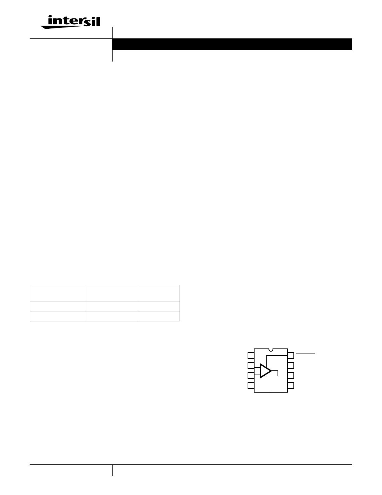
Pinout
HS-1145RH
GDIP1-T8 (CERDIP)
OR CDIP2-T8 (SBDIP)
TOP VIEW
NC
1
2
-IN
+IN
V-
1
CAUTION: These devices are sensitive to electrostatic discharge; follow proper IC Handling Procedures.
1-888-INTERSIL or 321-724-7143 | Copyright © Intersil Corporation 1999
-
+
3
4
8
DISABLE
7
V+
6
OUT
5
NC

HS-1145RH
Application Information
Optimum Feedback Resistor
Although a current feedback amplifier’s bandwidth
dependency on closed loop gain isn’t as severe as that of a
voltage feedback amplifier, there can be an appreciable
decrease in bandwidth at higher gains. This decrease may
be minimized by taking advantage of the current feedback
amplifier’s unique relationship between bandwidth and R
All current feedback amplifiers require a feedback resistor,
even for unity gain applications, and R
, in conjunction with
F
the internal compensation capacitor, sets the dominant pole
of the frequency response. Thus, the amplifier’sbandwidth is
inversely proportional to R
optimized for R
= 510Ω at a gain of +2. Decreasing R
F
. The HS-1145RH design is
F
decreases stability, resulting in excessive peaking and
overshoot (Note: Capacitive feedback will cause the same
problemsdue to the feedbackimpedance decrease at higher
frequencies). At higher gains, however, the amplifier is more
stable so R
can be decreased in a trade-off of stability for
F
bandwidth.
The table below lists recommended R
values for various
F
gains, and the expected bandwidth. For a gain of +1, a
resistor (
+R
) in series with +IN is required to reduce gain
S
peaking and increase stability.
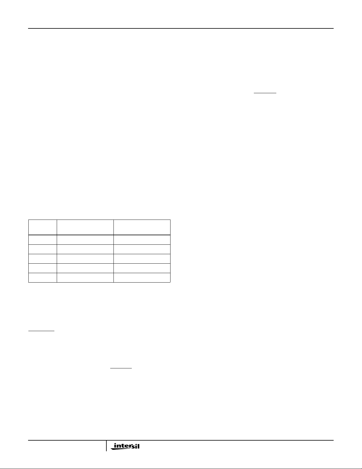
GAIN
(ACL) R
-1 425 300
+1 510 (+RS = 510Ω) 270
+2 510 330
+5 200 300
+10 180 130
(Ω)
F
BANDWIDTH
(MHz)
Non-Inverting Input Source Impedance
For best operation, the DC source impedance seen by the
non-inverting input should be ≥50Ω. This is especially
important in inverting gain configurations where the noninverting input would normally be connected directly to GND.
DISABLE Input TTL Compatibility
The HS-1145RH derives an internal GND reference for the
digital circuitry as long as the power supplies are symmetrical
about GND. With symmetrical supplies the digital s witching
threshold (V
ensures the TTL compatibility of the
asymmetrical supplies (e.g., +10V, 0V) are utilized, the
switching threshold becomes:
V
TH
and the V
= (VIH + VIL)/2 = (2.0 + 0.8)/2) is 1.4V, which
TH
DISABLE input. If
V+ V-+
------------------- 1.4V+=
2
and VIL levels will be VTH± 0.6V, respectively.
IH
.
F
F
Optional GND Pad (Die Use Only) for TTL
Compatibility
The die version of the HS-1145RH provides the user with a
GND pad for setting the disable circuitry GND reference.
With symmetrical supplies the GND pad may be left
unconnected, or tied directly to GND. If asymmetrical
supplies (e.g., +10V, 0V) are utilized, and TTL compatibility
is desired, die users must connect the GND pad to GND.
With an external GND,the
DISABLE input is TTL compatible
regardless of supply voltage utilized.
Pulse Undershoot and Asymmetrical Slew Rates
The HS-1145RH utilizes a quasi-complementary output
stage to achieve high output current while minimizing
quiescent supply current. In this approach, a composite
device replaces the traditional PNP pulldown transistor. The
composite device switches modes after crossing 0V,
resulting in added distortion for signals swinging below
ground, and an increased undershoot on the negative
portion of the output waveform (See Figures 5, 8, and 11).
This undershoot isn’t present for small bipolar signals, or
large positive signals. Another artifact of the composite
device is asymmetrical slew rates for output signals with a
negative voltage component. The slew rate degrades as the
output signal crosses through 0V (See Figures 5, 8, and 11),
resulting in a slower overall negative slew rate. Positive only
signals have symmetrical slew rates as illustrated in the
large signal positive pulse response graphs (See Figures 4,
7, and 10).
PC Board Layout
This amplifier’s frequency response depends greatly on the
care taken in designing the PC board. The use of low
inductance components such as chip resistors and chip
capacitors is strongly recommended, while a solid
ground plane is a must!
Attention should be given to decoupling the power supplies.
A large value (10µF) tantalum in parallel with a small value
(0.1µF) chip capacitor works well in most cases.
Terminated microstrip signal lines are recommended at the
device’s input and output connections. Capacitance,
parasitic or planned, connected to the output must be
minimized, or isolated as discussed in the next section.
Care must also be taken to minimize the capacitance to
ground at the amplifier’s inverting input (-IN), as this
capacitance causes gain peaking, pulse overshoot, and if
large enough, instability. To reduce this capacitance, the
designer should remove the ground plane under traces
connected to -IN, and keep connections to -IN as short as
possible.
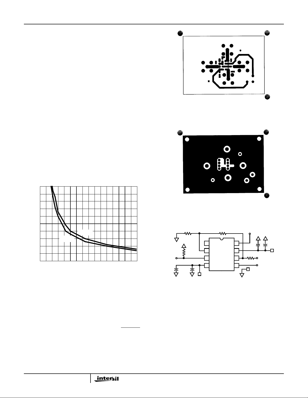
An example of a good high frequency layout is the
Evaluation Board shown in Figure 2.
2

HS-1145RH
Driving Capacitive Loads
Capacitive loads, such as an A/D input, or an improperly
terminated transmission line will degrade the amplifier’s
phase margin resulting in frequency response peaking and
possible oscillations. In most cases, the oscillation can be
avoided by placing a resistor (R
prior to the capacitance.
Figure 1 details starting points for the selection of this
resistor. The points on the curve indicate the R
combinations for the optimum bandwidth, stability, and
settling time, but experimental fine tuning is recommended.
Picking a point above or to the right of the curve yields an
overdampedresponse, while points belowor left of the curve
indicate areas of underdamped performance.
R
and CL form a low pass network at the output, thus
S
limiting system bandwidth well below the amplifier bandwidth
of 270MHz (for A
= +1). By decreasing RSas CLincreases
V
(as illustrated in the curves), the maximum bandwidth is
obtained without sacrificing stability. In spite of this, the
bandwidth decreases as the load capacitance increases. For
example, at A
= +1, RS = 62Ω, CL = 40pF, the overall
V
bandwidth is limited to 180MHz, and bandwidth drops to
75MHz at A
= +1, RS = 8Ω, CL = 400pF.
V
) in series with the output
S
and C
S
L
V
H
1
+IN
FIGURE 2A. TOP LAYOUT
OUT
V
L
V+
V-
GND
50
40
30
20
AV = +2
10
SERIES OUTPUT RESISTANCE (Ω)
0
0 100 200 300 400
AV = +1
150 250 35050
LOAD CAPACITANCE (pF)
FIGURE 1. RECOMMENDED SERIES OUTPUT RESISTOR vs
LOAD CAPACITANCE
Evaluation Board
The performance of the HS-1145RH maybe evaluatedusing
the HFA11XX Evaluation Board.
The layoutand schematic of the board are shown in Figure 2.
The V
connection may be used to exercise the DISABLE
H
pin, but note that this connection has no 50
order evaluation boards (part number HFA11XXEVAL),
please contact your local sales office.
Ω termination. To
FIGURE 2B. BOTTOM LAYOUT
10µF
510 510
R
1
50Ω
IN
0.1µF
-5V
1
2
3
4
GND
V
H
8
0.1µF
7
50Ω
6
5
GND
OUT
V
L
10µF
+5V
FIGURE 2C. SCHEMATIC
FIGURE 2. EVALUATION BOARD SCHEMATIC AND LAYOUT
3
 Loading...