Intersil Corporation HS-1135RH Datasheet

HS-1135RH
Data Sheet August 1999
Radiation Hardened, High Speed, Low
Power Current Feedback Amplifier with
Programmable Output Limiting
The HS-1135RH is a radiation hardened, high speed, low
power current feedback amplifier built with Intersil’s
proprietary complementary bipolar UHF-1(DI bonded wafer)
process. They are QML approved and processed in full
compliance with MIL-PRF-38535. This amplifier features
user programmable output limiting, via the V
and VL pins.
H
The HS-1135RH is the ideal choice for high speed, low
power applications requiring output limiting (e.g., flash A/D
drivers), especially those requiring fast overdrive recovery
times. The limiting function allows the designer to set the
maximum and minimum output levelsto protect downstream
stages from damage or input saturation. The subnanosecond overdrive recovery time ensures a quick return
to linear operation following an overdrive condition.
Component and composite video systems also benefit from
this op amp’s performance, as indicated by the gain flatness,
and differential gain and phase specifications.
Specifications for Rad Hard QML devices are controlled
by the Defense Supply Center in Columbus (DSCC). The
SMD numbers listed here must be used when ordering.
Detailed Electrical Specifications for these devices are
contained in SMD 5962-96767. A “hot-link” is provided
on our homepage for downloading.
http://www.intersil.com/spacedefense/space.htm
Ordering Information
INTERNAL
ORDERING NUMBER
5962F9676701VPA HS7-1135RH-Q -55 to 125
5962F9676701VPC HS7B-1135RH-Q -55 to 125
HS7-1135RH/PROTO HS7-1135RH/PROTO -55 to 125
MKT. NUMBER
TEMP. RANGE
(oC)
File Number 4099.2
Features
• Electrically Screened to SMD # 5962-96767
• QML Qualified per MIL-PRF-38535 Requirements
• User Programmable Output Voltage Limiting
• Fast Overdrive Recovery . . . . . . . . . . . . . . . . . <1ns (Typ)
• Low Supply Current . . . . . . . . . . . . . . . . . . . . 6.9mA (Typ)
• Wide -3dB Bandwidth. . . . . . . . . . . . . . . . . .360MHz (Typ)
• High Slew Rate. . . . . . . . . . . . . . . . . . . . . .1200V/µs (Typ)
• High Input Impedance . . . . . . . . . . . . . . . . . . . 2MΩ (Typ)
• Excellent Gain Flatness (to 50MHz). . . . . . ±0.07dB (Typ)
• Total Gamma Dose. . . . . . . . . . . . . . . . . . . . 300kRAD(Si)
• Latch Up. . . . . . . . . . . . . . . . . . . . . None (DI Technology)
Applications
• Flash A/D Driver
• Video Switching and Routing
• Pulse and Video Amplifiers
• Wideband Amplifiers
• RF/IF Signal Processing
• Imaging Systems
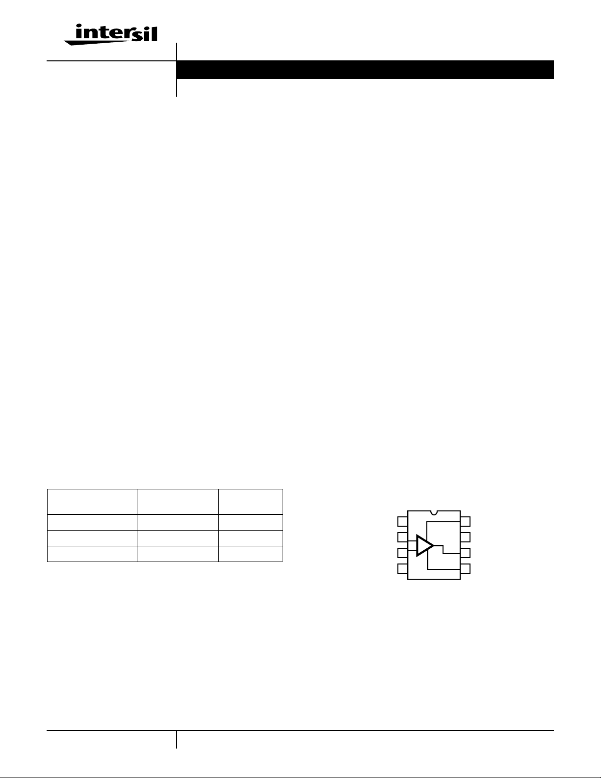
Pinout
HS-1135RH
GDIP1-T8 (CERDIP)
OR CDIP2-TI (SBDIP)
TOP VIEW
NC
-IN
+IN
1
2
-
+
3
4
V-
8
V
H
7
V+
6
OUT
5
V
L
1
CAUTION: These devices are sensitive to electrostatic discharge; follow proper IC Handling Procedures.
1-888-INTERSIL or 321-724-7143 | Copyright © Intersil Corporation 1999

HS-1135RH
Clamp Operation
General
The HS-1135RH features user programmable output clamps
to limit output voltageexcursions. Clamping action is obtained
byapplying voltagesto the V
of the amplifier. V
sets the upper output limit, while VL sets
H
the lower clamp lev el. If the amplifier tries to drive the output
above V
voltage at V
, or below VL, the clamp circuitry limits the output
H
or VL ( the clamp accuracy), respectively. The
H
low input bias currents of the clamp pins allow them to be
driven by simple resistive divider circuits, or active elements
such as amplifiers or DACs.
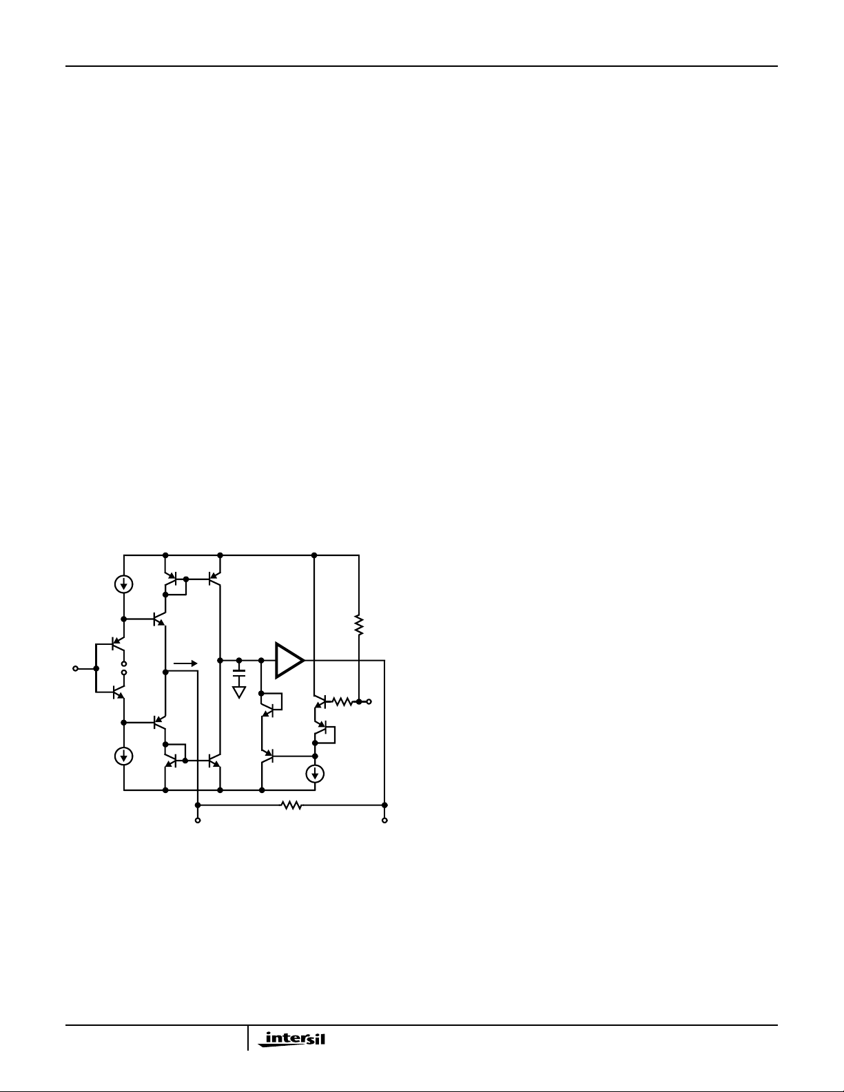
Clamp Circuitry
Figure 1 shows a simplified schematic of the HS-1135RH
input stage, and the high clamp (V
current feedback amplifiers, there is a unity gain buffer (Q
- QX2) between the positive and negative inputs. This buffer
forces -IN to track +IN, and sets up a slewing current of (V
-V
)/RF. This current is mirrored onto the high
OUT
IN
impedance node (Z) by Q
voltage and fed to the output via another unity gain buffer. If
no clamping is utilized, the high impedance node may swing
within the limits definedby Q
output reaches it’s quiescent value, the current flowing
through -IN is reduced to only that small current (-I
required to keep the output at the final voltage.
Q
P3
Q
N2
Q
P1
I
N1
CLAMP
Q
P2
Q
N3
V-
+IN
FIGURE 1. HS-1135RH SIMPLIFIED VH CLAMP CIRCUITRY
VV+
Q
Tracing the path from V
clamp voltage on the high impedance node. V
by 2V
(QN6 and QP6) to set up the base voltage on QP5.
BE
QP5 begins to conduct whenever the high impedance node
reaches a voltage equal to QP5’s base + 2V
QN5). Thus, QP5 clamps node Z whenever Z reaches V
R1 provides a pull-up network to ensure functionality with
and VLterminals (pins8 and5)
H
) circuitry. As with all
H
, where it is converted to a
X3-QX4
and QN4. Note that whenthe
P4
BIAS
V+
Q
P4
50K
(30K
Z
Q
N5
Q
P5
Q
N4
-IN V
to Z illustrates the effect of the
H
(EXTERNAL)
FOR VL)
+1
Q
N6
200Ω
Q
P6
R
F
decreases
H
(QP5 and
BE
X1
)
R
1
V
H
OUT
.
H
the clamp inputs floating. A similar description applies to the
symmetrical low clamp circuitry controlled by V
.
L
When the output is clamped, the negative input continues to
source a slewing current (I
output to the quiescent voltage defined bythe input.Q
) in an attempt to force the
CLAMP
P5
must
sink this current while clamping, because the -IN current is
alwaysmirrored ontothe high impedance node. The clamping
current is calculated as (V
unity gain circuit with V
have I
increase by I
= (2-1)/510Ω = 1.96mA. Note that ICC will
CLAMP
when the output is clamp limited.
CLAMP
- V
-IN
=2V,VH= 1V,and RF= 510Ω would
IN
)/RF. As an example, a
OUT
Clamp Accuracy
The clamped output voltage will not be exactly equal to the
voltage applied to V
or VL. Offset errors, mostly due to V
H
BE
mismatches, necessitate a clamp accuracy parameter which is
foundin the device specifications.Clamp accuracyis a function
of the clamping conditions. Referring again to Figure 1, it can
-
be seen that one component of clamp accuracy is the V
mismatchbetween the QX6transistors,and the QX5transistors.
BE
If the transistors always ran at the same current level there
would be no V
inaccuracy. The Q
current, but as described earlier, the current through Q
equivalent to I
causing the clampedoutput voltageto increase aswell. I
is a function of the overdrive le v el(V
R
,so clamp accuracy degrades as the overdrive increases, or
F
as R
decreases. As an example, the specified accuracy of
F
±60mVfor a 2Xoverdrivewith R
for R
= 240Ω at the same ov erdrive , or to±250mV for a 3X
F
overdrive with R
mismatch, and no contribution to the
BE
transistors are biased at a constant
X6
. VBE increases as I
CLAMP
= 510Ω.
F
F
CLAMP
-IN-VOUTCLAMPED
= 510Ωdegradesto ±220mV
X5
increases,
CLAMP
) and
is
Consideration must also be given to the fact that the clamp
voltages have an effect on amplifier linearity. The
“Nonlinearity Near Clamp Voltage” curve in the data sheet
illustrates the impact of several clamp levels on linearity.
Clamp Range
Unlike some competitor devices, both VH and VL have usable
ranges that cross 0V. While V
must be more positive than VL,
H
both may be positive or negativ e , within the range restrictions
indicated in the specifications. For e xample, the HS-1135RH
could be limited to ECL output levels bysetting V
V
= -1.8V. VH and VL may be connected to the same voltage
L
= -0.8V and
H
(GND for instance) but the result won’t be in a DC output
voltage from an AC input signal. A 150- 200mV AC signal will
still be present at the output.
Recovery from Overdrive
The output voltage remains at the clamp level as long as the
overdrive condition remains. When the input voltage drops
below the overdrive level (V
CLAMP/AVCL
return to linear operation. A time delay, known as the
Overdrive Recovery Time, is required for this resumption of
linear operation. The plots of “Unclamped Performance” and
“Clamped Performance” highlight the HS-1135RH’s
) the amplifier will
2
 Loading...