Intersil Corporation HS-1115RH Datasheet

August 1996
HS-1115RH
Radiation Hardened, High Speed, Low Power
Output Limiting, Closed-Loop-Buffer Amplifier
Features
• Electrically Screened to SMD 5962F9678501VPA
• MIL-PRF-38535 Class V Compliant
• User Programmable Output Voltage Limiting
• User Programmable For Closed-Loop Gains of +1, -1
or +2 Without Use of External Resistors
• Standard Operational Amplifier Pinout
• Fast Overdrive Recovery. . . . . . . . . . . . . . . . <1ns (Typ)
• Low Supply Current. . . . . . . . . . . . . . . . . . 6.9mA (Typ)
• Excellent Gain Accuracy. . . . . . . . . . . . . .0.99V/V (Typ)
• Wide -3dB Bandwidth . . . . . . . . . . . . . . . 225MHz (Typ)
• Fast Slew Rate . . . . . . . . . . . . . . . . . . . . 1135V/µs (Typ)
• High Input Impedance . . . . . . . . . . . . . . . . . . 1MΩ (Typ)
• Excellent Gain Flatness (to 50MHz) . . . . . ±0.1dB (Typ)
• Total Gamma Dose. . . . . . . . . . . . . . . . . . 300K RAD (Si)
• Neutron Damage . . . . . . . TBD (When Tests Complete)
• Latch Up . . . . . . . . . . . . . . . . . . . None (DI Technology)
Applications
• Flash A/D Driver
• Video Switching and Routing
• Pulse and Video Amplifiers
• Wideband Amplifiers
• RF/IF Signal Processing
• Imaging Systems
Ordering Information
TEMP.
PART NUMBER
5962F9678501VPA -55 to 125 8 Ld CERDIP GDIP1-T8
HFA1115IP
(Sample)
HFA11XXEVAL Evaluation Board
RANGE (oC) PACKAGE PKG. NO.
-40 to 85 8 Ld PDIP E8.3
Description
The HS-1115RH is a radiation hardened, high speed closed
loop buffer featuring both user programmable gain and output limiting. They are QML approved and processed in full
compliance with MIL-PRF-38535. Manufactured in proprietary, complementary bipolar UHF-1 (DI bonded wafer) process, the HS-1115RH also offers a wide -3dB bandwidth of
225MHz, very fast slew rate, excellent gain flatness and high
output current.
This buffer is the ideal choice for high frequency applications
requiring output limiting, especially those needing ultra fast
overload recovery times. The limiting function allows the
designer to set the maximum positive and negative output
levels, thereby protecting later stages from damage or input
saturation. The HS-1115RH also allows for voltage gains of
+2, +1, and -1, without the use of external resistors. Gain
selection is accomplished via connections to the inputs, as
described in the “Application Information” text. The result is a
more flexible product, fewer part types in inventory, and
more efficient use of board space.
Compatibility with existing op amp pinouts provides flexibility to
upgrade low gain amplifiers, while decreasing component
count. Unlike most buffers, the standard pinout provides an
upgrade path should a higher closed loop gain be needed at a
future date.
Detailed electrical specifications are contained in SMD
5962F9678501VPA, available on the Intersil Website or
AnswerFAX systems (document #967850)
A Cross Reference Table is available on the Intersil Website
for conversion of Intersil Part Numbers to SMDs. The address is
(www.intersil.com/datasheets/smd/smd_xref.html). SMD
numbers must be used to order Radiation Hardened Products.
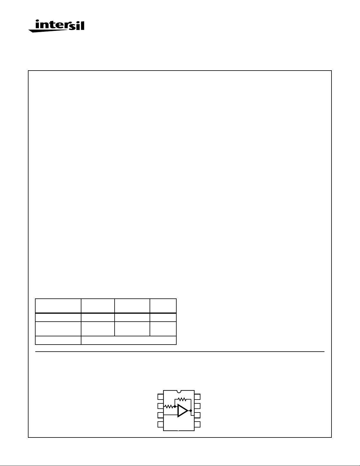
Pinout
HS-1115RH
MIL-STD-1835, GDIP1-T8
(PDIP, CERDIP)
TOP VIEW
350
350
-
+
1
8
V
H
7
V+
6
OUT
5
V
L
NC
1
2
-IN
3
+IN
4
V-
CAUTION: These devices are sensitive to electrostatic discharge; follow proper IC Handling Procedures.
1-888-INTERSIL or 321-724-7143 | Copyright © Intersil Corporation 1999
File Number 4098.1

HS-1115RH
Application Information
Closed Loop Gain Selection
The HS-1115RH features a novel design which allows the
user to select from three closed loop gains, without any
external components. The result is a more flexible product,
fewer part types in inventory, and more efficient use of board
space.
This “buffer” operates in closed loop gains of -1, +1, or +2, and
gain selection is accomplished via connections to the ±inputs.
Applying the input signal to +IN and floating -IN selects a gain
of +1 (see next section for layout caveats), while grounding -IN
selects a gain of +2. A gain of -1 is obtained by applying the
input signal to -IN with +IN grounded.
The table below summarizes these connections:
GAIN
(ACL)
-1 GND Input
+1 Input NC (Floating)
+2 Input GND
+INPUT (PIN 3) -INPUT (PIN 2)
Unity Gain Considerations
Unity gain selection is accomplished by floating the -Input of
the HS-1115RH. Anything that tends to short the -Input to
GND, such as stray capacitance at high frequencies, will
cause the amplifier gain to increase toward a gain of +2. The
result is excessive high frequency peaking, and possible
instability. Even the minimal amount of capacitance associated with attaching the -Input lead to the PCB results in
approximately 3dB of gain peaking. At a minimum this
requires due care to ensure the minimum capacitance at the
-Input connection.
Table 1 lists five alternate methods for configuring the
HS-1115RH as a unity gain buffer, and the corresponding
performance. The implementations vary in complexity and
involve performance trade-offs. The easiest approach to
implement is simply shorting the two input pins together, and
applying the input signal to this common node. The amplifier
bandwidth drops from 400MHz to 200MHz, but excellent
gain flatness is the benefit. Another drawback to this
approach is that the amplifier input noise voltage and input
offset voltage terms see a gain of +2, resulting in higher
noise and output offset voltages. Alternately, a 100pF
capacitor between the inputs shorts them only at high
frequencies, which prevents the increased output offset
voltage but delivers less gain flatness.
CONNECTIONS
Another straightforward approach is to add a 620Ω resistor
in series with the positive input. This resistor and the
HS-1115RH input capacitance form a low pass filter which
rolls off the signal bandwidth before gain peaking occurs.
This configuration was employed to obtain the datasheet AC
and transient parameters for a gain of +1.
PC Board Layout
The frequency response of this amplifier depends greatly on
the amount of care taken in designing the PC board. The
use of low inductance components such as chip resistors and chip capacitors is strongly recommended,
while a solid ground plane is a must!
Attention should be given to decoupling the power supplies.
A large value (10µF) tantalum in parallel with a small value
(0.1µF) chip capacitor works well in most cases.
Terminated microstrip signal lines are recommended at the
input and output of the device. Capacitance directly on the
output must be minimized, or isolated as discussed in the
next section.
For unity gain applications, care must also be taken to
minimize the capacitance to ground seen by the amplifier’s
inverting input. At higher frequencies this capacitance will
tend to short the -INPUT to GND, resulting in a closed loop
gain which increases with frequency. This will cause
excessive high frequency peaking and potentially other
problems as well.
An example of a good high frequency layout is the
Evaluation Board shown in Figure 1.
Driving Capacitive Loads
Capacitive loads, such as an A/D input, or an improperly
terminated transmission line will degrade the amplifier’s
phase margin resulting in frequency response peaking and
possible oscillations. In most cases, the oscillation can be
avoided by placing a resistor (R
prior to the capacitance.
R
and CLform a low pass network at the output, thus limit-
S
ing system bandwidth well below the amplifier bandwidth of
225MHz. By decreasing R
bandwidth is obtained without sacrificing stability.
) in series with the output
S
as CLincreases the maximum
S
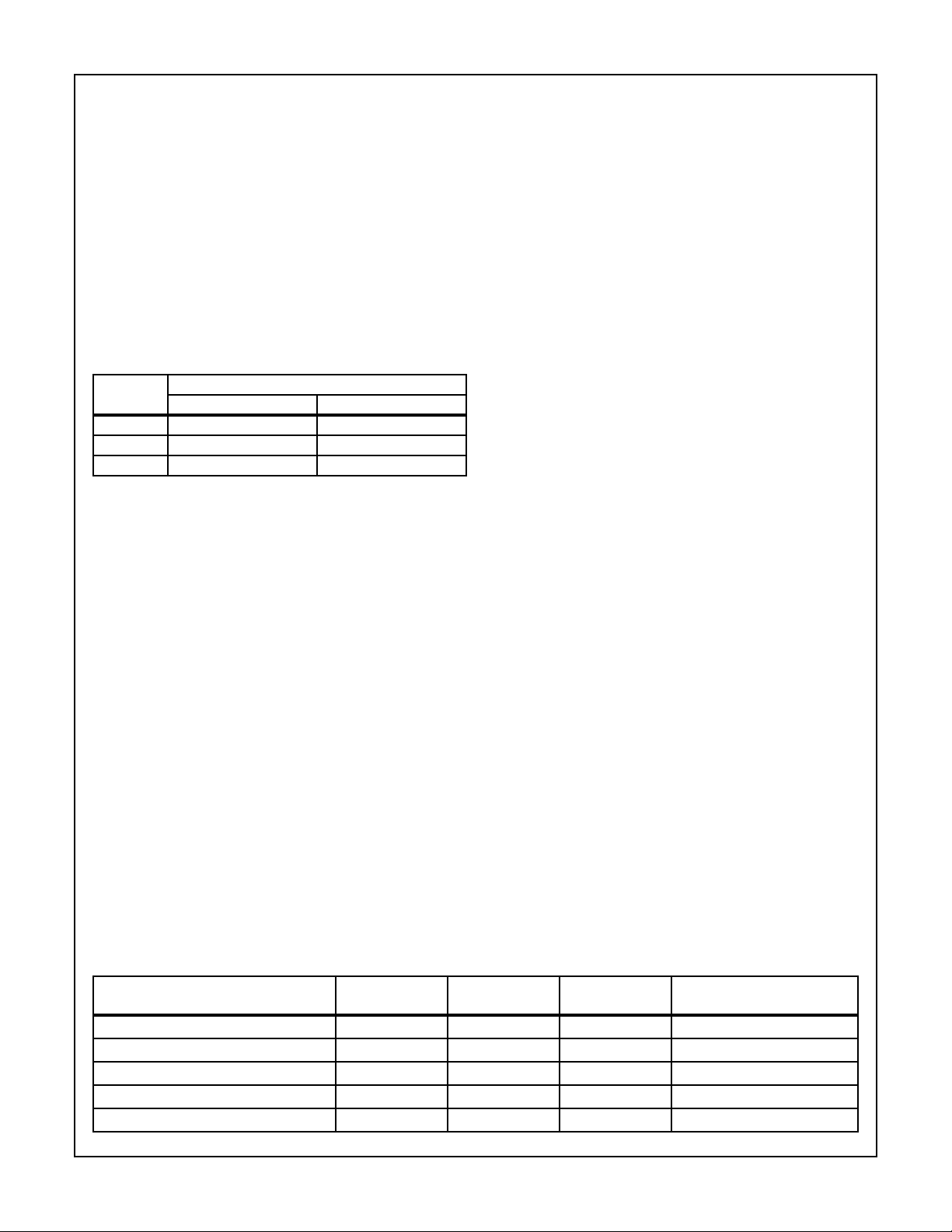
TABLE 1. UNITY GAIN PERFORMANCE FOR VARIOUS IMPLEMENTATIONS
±0.1dB GAIN FLATNESS
APPROACH PEAKING (dB) BW (MHz) +SR/-SR (V/µs)
Remove Pin 2 2.5 400 1200/850 20
+RS= 620Ω 0.6 170 1125/800 25
+RS= 620Ω and Remove Pin 2 0 165 1050/775 65
Short Pins 2, 3 0 200 875/550 45
100pF cap. between pins 2, 3 0.2 190 900/550 19
(MHz)
2
 Loading...